BEAMING AND LOCALIZATION OF
ELECTROMAGNETIC WAVES IN PERIODIC
STRUCTURES
A DISSERTATION
SUBMITTED TO THE DEPARTMENT OF PHYSICS AND THE INSTITUTE OF ENGINEERING AND SCIENCE
OF BILKENT UNIVERSITY
IN PARTIAL FULFILLMENT OF THE REQUIREMENTS FOR THE DEGREE OF
DOCTOR OF PHILOSOPHY
By
Hümeyra Çağlayan
ii
I certify that I have read this thesis and that in my opinion it is fully adequate, in scope and in quality, as a dissertation for the degree of Doctor of Philosophy.
___________________________________ Prof. Dr. Ekmel Özbay (Supervisor)
I certify that I have read this thesis and that in my opinion it is fully adequate, in scope and in quality, as a dissertation for the degree of Doctor of Philosophy.
___________________________________ Prof. Dr. Atilla Erçelebi
I certify that I have read this thesis and that in my opinion it is fully adequate, in scope and in quality, as a dissertation for the degree of Doctor of Philosophy.
___________________________________ Assoc. Prof. Dr. Ceyhun Bulutay
iii
I certify that I have read this thesis and that in my opinion it is fully adequate, in scope and in quality, as a dissertation for the degree of Doctor of Philosophy.
___________________________________ Assoc. Prof. Dr. Vakur B. Ertürk
I certify that I have read this thesis and that in my opinion it is fully adequate, in scope and in quality, as a dissertation for the degree of Doctor of Philosophy.
___________________________________ Assist. Prof. Dr. Hamza Kurt
Approved for the Institute of Engineering and Science:
___________________________________ Prof. Dr. Mehmet Baray,
iv
ABSTRACT
BEAMING AND LOCALIZATION OF
ELECTROMAGNETIC WAVES IN PERIODIC
STRUCTURES
Hümeyra Çağlayan
PhD in Physics
Supervisor: Prof. Dr. Ekmel Özbay June, 2010
We want to manipulate light for several applications: microscopy, data storage, leds, lasers, modulators, sensor and solarcells to make our life healthier, easier or more comfortable. However, especially in small scales manipulating light have many difficulties. We could not focus or localize light into subwavelength dimensions easily, which is the key solution to beat today’s devices both in performance and cost. Achievements in three key research fields may provide the answer to these problems. These emerging research fields are metamaterials, photonic crystals and surface plasmons. In this thesis, we investigated beaming and localization of electromagnetic waves in periodic structures such as: subwavelength metallic gratings, photonic crystals and metamaterials. We studied off-axis beaming from both a metallic subwavelength aperture and photonic crystal waveguide at microwave regime. The output surfaces are designed asymmetrically to change the beaming angle. Furthermore, we studied frequency dependent beam steering with a photonic crystal with a surface defect layer made of dimmers. The dispersion diagram reveals that the dimer-layer supports a surface mode with negative slope. Thus, a photonic crystal based surface wave structure that acts as a frequency dependent leaky wave antenna was presented. Additionally, we investigated metamaterial based cavity systems. Since the unit cells of
v
metamaterials are much smaller than the operation wavelength, we observed subwavelength localization within these metamaterial cavity structures. Moreover, we introduced coupled-cavity structures and presented the transmission spectrum of metamaterial based coupled-cavity structures. Finally, we demonstrated an ultrafast bioassay preparation method that overcomes the today’s bioassay limitations using a combination of low power microwave heating and split ring resonator structures.
Keywords: Surface Plasmons, Off-Axis Beaming, Photonic Crystal, Surface Mode,
Beam Steering, Backward Leaky Wave, Metamaterial, Split Ring Resonator,
Composite Metamaterial, Negative Permittivity, Negative Permeability,
vi
ÖZET
PERİYODİK YAPILARDA ELEKTROMAGNETİK
DALGALARIN YÖNLENDİRİLMESİ VE
LOKALİZASYONU
Hümeyra Çağlayan
Fizik, Doktora
Tez Yöneticisi: Prof. Dr. Ekmel Özbay Haziran 2010
Hayatımızı daha kolay, konforlu ve sıhhatli yapmak için mikroskop, veri saklama, LED, lazer, modulator, sensor ve güneş pilleri gibi çok çeşitleri araçlarda elektromanyetik dalgaların isteğimize uygun biçimde yönlendirmek istiyoruz. Fakat, özellikle çok küçük boyutlarda elektromanyetik dalgaları isteğimize uygun şekilde yönlendirmek çok zordur. Bugünkü kullandığımız pek çok cihazı performans ve maliyet açısından daha iyileriyle değiştirmek içinse gerekli olan en önemli çözüm olan elektromanyetik dalgaları dalgaboyu-altı boyutta odaklamak ve yönlendirmektir işlemini kolayca yapamıyoruz. Üç önemli çalışma alanlarındaki başarılar bu soruna çözüm olabilir. Bu gelişmekte olan çalışma alanları: metamalzemeler, fotonik kristallar ve yüzey plazmonlarıdır. Bu tezde, dalgaboyu-altı metalik ızgaralı yapılar, fotonik kristaller ve metamalzemeler gibi periyodik yapılarda elektroanyetik dalgaların yönlendirilmesi ve lokalizasyonu incelendi. Hem metalik dagaboyu-altı yapıları hem de fotonik kristaldalga kılavuzu ile eksenden sapmış yönledirme mikrodalga boyutunda araştırıldı. Çıkış yüzeyi yönlendirme açısını değiştirmek amacıyla asimetrik olarak tasarlandı. Ayrıca, yüzey yapısı değiştirilmiş fotonik kristal yapıları ile frekansa bağlı yönlendirme çalışıldı. Dispersiyon diyagramı ile değiştirilmiş olan yüzey yapısının negatif
vii
eğime sahip yüzey modu ortaya çıkarıldı. Bu nedenle, fotonik kristal bazlı yüzey dalgaları ile frekansa bağlı sızan dalga antenlerinin çalışma sisteminin aynı olduğu gösterildi. Bütün bunlara ek olarak, metamalzeme bazlı kavite yapıları araştırıldı. Metamazelme yapılarının birim hücreleri çalışma dalga boyundan çok küçük olduğu için, dalgaboyu-altı lokalizasyon gözlendi. Ayrıca bağlı-kavite yapıları incelendi. Son olarak, günümüzde kullanılan biyolojik tahlil metodlarının limitlerini aşabilen çok hızlı biyolojik tahlil metodu düşük güçlü mikrodalga ısınma ve yarıklı halka rezönatötleri kullanılarak gösterildi.
Anahtar Kelimeler: Yüzey Plazmonları, Eksenden sapmış yönlendirme, Fotonik
Kristal, Yüzey Modu, Işın yönlendirme, Ters sızan dalga, Metamalzeme, Yarıklı halka rezonatörü, Kompozit Metamalzeme, Negatif Permeabilite, Negatif Permitivite, Metamalzeme bazlı Kavite, Dalgaboyu-altı lokalizasyon, Çok hızlı Biyolojik tahlil.
viii
Acknowledgements
It is my pleasure to express my deepest gratitude and respect to Prof. Dr. Ekmel Ozbay for his invaluable guidance, helpful suggestions and endless support. His personal and academic virtue shaped my academic personality and changed my approach to scientific study.
I would like to thank to the members of my thesis committee, Prof. Dr. Atilla Erçelebi, Assoc. Prof. Dr. Ceyhun Bulutay, Assoc. Prof. Dr. Vakur B. Ertürk, and Assit. Prof. Dr. Hamza Kurt, for reading the manuscript and commenting on the thesis.
I would like to express my special thanks and gratitude to Dr. İrfan Bulu for his continues support, encouragement and valuable ideas towards the realization of this thesis work.
I am very fortunate to have been a member of the Özbay group. This thesis would never been succesful with the endless help of the Özbay group members. I had a chance to collaborate with Dr. Koray Aydın, Evrim Çolak, Atilla Özgür Çakmak, Dr. Zhaofeng Li, Kamil Boratay Alıcı and Semih Çakmakyapan. Indeed, all of the people with whom I’ve overlapped in the Özbay group have contributed to my academic life. Thank you all.
I would like to thank the members of Nanotechnology Research Center and Advanced Research Laboratory for making my life easier. I am also thankful to my professors and friends in the Department of Physics.
ix
I am grateful to all of our collaborators for sharing our enthusiasm for the projects, and giving their time and best effort to contribute to our joint work.
I would also like to thank my close friend Evren Karakaya for her help, understanding and friendship.
Special thanks go to my mom, father and sisters for their love, encouragement and care. I cannot imagine finishing all my achievements without their endless moral support.
Finally, thanks to my husband and to my son, Engin Yahya, for shining a different color onto my life. I dedicate this labor to my mom and my son.
x
Contents
ABSTRACT ... iv ÖZET ... vi Acknowledgements ... viii Contents ... x List of Figures ... xList of Tables ... xxi
1 Introduction ... 1
2 Off-Axis beaming from metallic gratings ... 5
2.1. Introduction ... 5
2.2. Surface Plasmon Polaritons ... 6
2.3. Directional beaming from a subwavelength metallic aperture ... 9
2.3.1. Simulation ... 11
2.3.2. Measurements ... 13
2.4. Off-axis beaming... 15
2.4.1. Origin of the off-axis beaming ... 20
3 Off-Axis directional beaming via photonic crystal surface modes ... 25
3.1. Introduction ... 25
3.2. Surface Propagating Modes of PCs ... 27
3.3. Directional beaming from PC Waveguide ... 30
xi
4 Frequency dependent steering with backward leaky waves ... 40
4.1. Introduction ... 40
4.2. Experimental Setup ... 42
4.3. Dispersion Diagram ... 44
4.4. Radiation properties of a source embedded in the PCD ... 45
4.5. Backward wave character and radiation property of the leaky mode excited in the dimer-layer ... 53
5 Metamaterial based cavities ... 57
5.1. Introduction ... 57
5.2. Negative Permittivity and Permeability ... 58
5.3. Split Ring Resonator structure ... 61
5.4. Composite Metamaterial Structure ... 65
5.5. Metamaterial based single cavity structure ... 66
5.6. Subwavelength Localization ... 72
5.7. Reduced Photon lifetime ... 73
5.8. 1D Fabry Perot resonator model ... 75
5.9. Metamaterial based coupled cavity systems ... 79
6 Ultrafast and sensitive bioassay ... 85
6.1. Introduction ... 85
6.2. Limitations of Bioassays ... 86
xii
6.4. Deposition of Silver Island Films inside the micro-cuvette of SRR
structures ... 89
6.5. Construction of colorimetric ELISA on SRR structures and HTS plates 90 6.6. Ultrafast and sensitive Bioassay ... 91
7 Conclusion ... 99
8 Bibliography ... 103
Appendix A ... 115
List of Figures
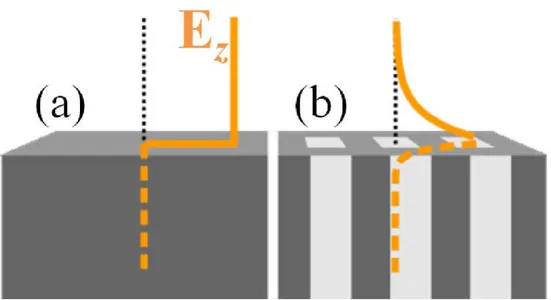
Figure 2.1: The charges and the EM field of SPs propagating on a surface in the x direction are shown schematically. The exponential dependence of the field Ez is seen on the right. Hy shows the
magnetic field in the y direction of the p-polarized wave. ... 7 Figure 2.2: Schematic representation of electric fields associated with a mode
propagating along the surface of a metal. (a) At microwave frequencies, the metal is almost perfectly conducting and the field (Ez) extends far beyond the metal. (b) By perforating the substrate
with an array of subwavelength holes, the field is localized near the interface. ... 8 Figure 2.3: (a) The reference sample (a metal plate with a subwavelength slit
in it), (b) a subwavelength slit surrounded by periodic gratings where w=2 mm, h=4 mm and p= 16 mm. ... 10 Figure 2.4: Experiment set up for angular distribution measurements. ... 12 Figure 2.5: The normalized measured and calculated angular transmission
distribution at the resonance frequency (14 GHz) in linear scale for (a) reference sample and (b) slit surrounded by periodic gratings. ... 14 Figure 2.6: The structures used in this work where a=7 mm, b=8 mm, c=11
mm, and t=16 mm. The slit widths were 2 mm and the grating heights were 4 mm. All of them have the same input surface grating period of 16 mm in order to couple the SPs. ... 15 Figure 2.7: The beaming angle is steered for structures with grating periods
only on one side of the output surface. The beam is mostly directed to the negative side for (a) Sample 1 and positive side for (b) Sample 2 at 14.5 GHz (20.7 mm). ... 16
xi
Figure 2.8: The calculated transmission throughout Sample 3 shows that off-axis and directional beaming is possible by using metallic asymmetric gratings on the output surface at SP resonance (14.5 GHz). ... 18 Figure 2.9: By use of a metallic structure with a subwavelength aperture at the
center and the grating periods of 14 mm and 22 mm on the different sides of the output surface, we observed off-axis directional beaming with an FWHM of 10o and the beaming angle of 15o. It is possible to steer the beaming angle by arranging the grating periods of the output surface of the metallic structure. ... 19 Figure 2.10: FDTD mode pattern showing the coupling between the top and
bottom surface at the resonance frequency. ... 19 Figure 2.11: Calculated E-field and far field for subwavelength apertures with
an input and output side grating period of 16 mm. ... 21 Figure 2.12: Calculated E-field and far field for subwavelength apertures with
an input side grating period of 16 mm. The projected direction of the diffracted beam is toward the waveguide channel for a structure with an output surface grating period of 14 mm. ... 22 Figure 2.13: Calculated E-field and far field for subwavelength apertures with
an input side grating period of 16 mm. The projected direction of the diffracted beam is away from the waveguide channel for a structure with an output surface grating period of 22 mm. ... 23 Figure 2.14: Calculated E-field and far field for subwavelength apertures with
an input side grating period of 16 mm. The off-axis beam was achieved with the combination of these structures (output surface grating is 14 mm and 22 mm on the different sides of the aperture). . 24 Figure 3.1: (a) A 3 dimensional PC made from alumina rods. Alumina rods are
xii
pigment in a butterfly wing which is blue due to PC (http://www.lpn.cnrs.fr/en/GOSS/CPOI.php). ... 26 Figure 3.2: Electric field intensity profiles of the modes supported by the finite
size PC: (a) mode decays in the air but extends in the PC, (b) mode extends in the air but decays in the PC and (c) mode extends in the air and the PC. (d) Surface mode: decays both in the air and PC; it is localized at the modified interface layer. These field profiles are calculated by using the plane wave expansion method. ... 28 Figure 3.3: (a) The TM (electric field parallel to the axis of the rods) band
structure of the infinite size PC (b) the TM band structure of the finite size (c) the TM band structure of the finite size PC when the radius of the rods at the surface of the PC is reduced to 0.76 mm. (d) zoomed view of the TM band structure of the finite size PC when the radius of the rods at the surface of the PC is reduced to 0.76 mm. ... 29 Figure 3.4: The measured intensity distribution at the exit side of the PC
waveguide. Y-axis is parallel to the PC surface. ... 31 Figure 3.5: Calculated field intensity when the surface corrugation is added to
the exit surface of the PC waveguide. ... 32 Figure 3.6: The measured intensity distribution at the exit side of the PC
waveguide when the corrugation and grating-like layer are added to the exit surface of the PC waveguide. Y-axis is parallel to the PC surface. ... 32 Figure 3.7: (a) Measured far field radiation pattern of the EM waves emitted
from PC waveguide at 12.45 GHz (b) Measured far field radiation pattern of EM waves emitted from the PC waveguide with surface corrugation and grating-like layer. ... 34
xiii
Figure 3.8: The 2D PC is constructed from a 43x11 square array of circular alumina rods (indicated as green dots). The crystal is 11 layers along the propagation direction. The radius of the rods in the modified layer (indicated as red dots) is half of the regular rods (0.76mm). The rods in the grating-like layer have equal radii of the bulk PC rods (indicated as blue dots). The asymmetric grating-like layer has a double period (22 mm) on one side and a triple period (33 mm) on the other side of the PC waveguide. ... 35 Figure 3.9: FDTD calculations of the transmission from the PC waveguide
exhibit off-axis beaming around 11 GHz. The periods of the grating like layer on the different sides of the waveguide were designed as 22 mm and 33 mm in order to steer the beaming angle... 36 Figure 3.10: The measured (a) and calculated (b) radiation patterns of the EM
waves emitted from the PC waveguide at 11.1 GHz. The right side of 90o stands for the side with grating-like layer period of 33 mm. .... 37 Figure 3.11: The measured intensity distribution at the exit side of the PC
waveguide when the corrugation and grating-like layer are added to the exit surface of the PC waveguide. Y-axis is parallel to the PC surface and positive side of the axis indicates the side of grating-like layer with period of 33mm. ... 38 Figure 4.1: (a) PC2 structure, (b) PC3 structure, (c) PCD structure, (d)
Experimental setup with the PCD, (e) side view of the monopole with the rods, (f) Single periodicity-cell of PC made of 5 layers (PC5), periodic along the x-direction (to be used in the simulations), (g) Single periodicity-cell consisting of the PC5 with a dimer on top, periodic along the x-direction, which is also used in the simulations, (h,i) images of the PCD that is constructed. ... 43
xiv
Figure 4.2: Dispersion diagram describing propagation along the x-direction. The surface mode in the dimer-layer (blue dot) resides inside the bandgap bounded by the air band (dash-dot) and the dielectric band (dashed with two dots) of the PC5 structure without dimer-layer. ... 45 Figure 4.3: RG for the PCD obtained by FDTD simulation (a), and by
measurement (b). Dashed lines represent the sample frequencies further investigated (magenta for Case 1, yellow for Case 2, black, green, and red for Cases3a, b, c, respectively). For each case, a polar plot of the radiation pattern is provided. Comparing Fig. 4.3(a) to Fig 4.3(b), the discrepancies (i.e., non-symmetric appearance especially at high frequencies) in the measurement RG are attributed to the artifacts of the manufactured PCD and to the non ideal amplitude and frequency (i.e., non-uniform AD) characteristics of the monopole source. ... 47 Figure 4.4: Normalized angular field distribution for Case 1 at a/λ=0.353. (a)
Simulation results obtained from the RG in Fig. 4.3(a) (b) Measurement results obtained from the RG in Fig. 4.3(b)... 48 Figure 4.5: Normalized angular field distribution for Case 2 at a/λ=0.373. (a)
Simulation results obtained from the RG in Fig. 4.3(a). (b) Measurement results obtained from the RG in Fig. 4.3(b)... 50 Figure 4.6: Angular field distribution for Case 3abc (shown in Fig. 4.3) at
frequencies a/λ=0.385 (black dotted line for Case 3a), a/λ=0.410
(green dashed line for Case 3b), and a/λ=0.438 (red solid line for
Case 3c). (a) Simulation results for the “far field” radiation pattern
which are performed by Rsoft Fullwave software (previously, the simulation RG evaluated at 1m from the center was given in Fig. 4.3(a)). (b) Measurement results from the RG in Fig. 4.3(b). This
xv
shows that measurements performed at 1m provide an estimate of the far field radiation pattern. ... 52 Figure 4.7: Calculated mode field profile for Case 2 and Case 3. (a) Case 2: the
surface wave (guided) frequency is a/λ=0.373, (b) Case 3: the radiative (leaky wave) frequency is a/λ=0.41. (c) Cross sections of the mode profiles (Figs. 4.7(a) and 4.7(b)) taken along x-direction passing through the center of the dimers are plotted in the same arbitrary units which is used in Fig. 4.4(a) and Fig 4.5(a). ... 53 Figure 4.8: The experimental setup for PCHD and the normalized AD
measurement. The angular field distribution is measured at a distance of 1m at frequencies of a/λ=0.373 (yellow dash-dotted line) which is the guiding frequency, and at the beaming frequencies which are a/λ=0.385 (black dotted line), a/λ=0.410 (green dashed line), a/λ=0.438 (red solid line). ... 54 Figure 4.9: Radiation Graph for the PC with a halved dimer-layer. (a)
Simulation, (b) Experimental result (yellow for Case 2, black, green, and red for Case 3a,b,c). The cross sections that are indicated by black, green, and red and yellow dashed lines are plotted in Fig. 4.8. ... 55 Figure 5.1: First metamaterials, constituted only by standard metals and
dielectrics, proposed by Pendry. (a) Thin-wire structure exhibiting negative ε and positive µ if E//z. (b) SRR structure exhibiting positive ε and negative μ if H⊥y. ... 59 Figure 5.2: (a) The unit cell of the SRR structure: a=4.95 mm, b=0.25 mm and
c=0.25mm. (b) The SRR structure has a bandgap between 5 and 7 GHz. However, the CRR structure transmits EM waves (black curve). Hence, the SRR structure exhibits µ<0 medium at these frequencies. ... 62
xvi
Figure 5.3: (a)The calculated effective ε and μ of the SRR structure by use of a retrieval procedure show that the SRR structure possesses effective ε>0, µ<0 from 5.0 to 7.0 GHz. (b) The calculated surface current density of the SRR structure at magnetic resonance frequency shows that the SRR structure behaves like a magnetic dipole. ... 64 Figure 5.4: (a) Unit cell of the CMM structure: c=1.6 mm (b) The CMM
structure transmits EM waves, because it has ε <0 and µ<0 between 5 and 7 GHz. ... 65 Figure 5.5: The calculated effective ε and μ of the SRR structure by use of a
retrieval procedure show that the CMM structure possesses effective ε<0, µ<0 from 5.4 to 7.0 GHz and ε<0, µ>0 from 7.0 to 9.4 GHz. ... 66 Figure 5.6: (a) Unit cell of the cavity structure: e=1 mm, f=5.4 mm. The unit
cells of metamaterials are much smaller than the operating wavelength. (b) The calculated effective ε and μ of the cavity structure by use of a retrieval procedure. ... 67 Figure 5.7: A cavity structure is introduced by replacing the center unit cell
with a positive-index medium. The cavity resonance is observed at 6.7 GHz 44.7 mm and 7.5 GHz 40 mm by the (a) SRR cavity structure and (b) the CMM cavity structure, respectively. ... 68 Figure 5.8: The calculated transmission for SRR cavity structure without loss
(red line), with loss on board only (blue line), and with loss on metal only (green line). The calculated loss free transmission of the SRR cavity resonance possesses the highest Q-factor. It decreases if the losses of the materials have been introduced (inset: zoomed to the cavity resonance frequency). ... 69 Figure 5.9: Four different defect structures used in this study: (a) D1: closed
xvii
(b) D2: closed ring only on the front side, (c) D3: cut wire only on the back side and, (d) D4: cut wire on both sides of the Teflon board. These defect structures were introduced in the center of the CMM structure. Therefore, there are four layers of a CMM structure in the forward and backward of the defect structures in the propagation direction. ... 70 Figure 5.10: We observed cavity modes in the transmission spectrum of the
CMM-based cavities (D1, D2, D3, and D4). The experiments (red line) are in good agreement with the CST Microwave calculations (black line). It is possible to design different CMM based cavity structures operating at different frequencies with different Q-factors. ... 71 Figure 5.11: The calculated electric field is highly localized at the cavity
region for (a) SRR cavity and (b) CMM cavity structures. Hence, the field at the cavity resonance is enhanced at the subwavelength λ/8 cavity region. (Red indicates the maximum, and blue indicates the minimum.) ... 73 Figure 5.12: The measured photon lifetime is 10 ns for SRR cavity structure
and 3.3 ns for CMM cavity structure. This also means that at the cavity resonance the effective group velocity is reduced by a factor of 67 for SRR cavity and 24 for CMM cavity when compared to the EM waves propagating in free space. ... 74 Figure 5.13: (a). The CMM based cavities can be treated as 1D FPRs with a
subwavelength cavity region at the center. (b). The calculated transmission from the model of the CMM based cavity (D3) structure using the 1D transfer matrix method (black line) and CST Microwave Studio (red line) are in good agreement. ... 76
xviii
Figure 5.14: The calculated total phase (T) around the cavity resonance shows that the resonance condition is satisfied at the resonance frequency for a CMM based cavity (D3) structure, just like in FPRs. ... 78 Figure 5.15: (a) The total two-cavity system contains two cavities and four
metamaterial unit cells at each side of each cavity (b) the total three-cavity system contains three cavities and four metamaterial unit cells in each side of the each cavity. ... 79 Figure 5.16: Measured (red curves) and calculated (black curves) transmission
spectra for (a) SRR based (b) CMM based two-coupled-cavity. The measured values of resonance frequencies are ω1=6.5 GHz
and ω2=6.9 GHz for the SRR based cavity structure and ω1=7.3
GHz and ω2=7.9 GHz for the CMM based cavity structure... 80
Figure 5.17: Measured (red curves) and calculated(black curves) transmission spectra for (a) SRR based (b) CMM based three-coupled-cavity. ... 82 Figure 5.18: (a) The calculated dispersion relation of the coupled cavity
structures is shown (black curves stand for the SRR based cavity and the red curves stand for the CMM cavity structure.) (b) The group velocity is two orders of magnitude smaller than the speed of light at the band center and vanishes at the band edges. ... 84 Figure 6.1: (a) Schematic depiction of copper SRR structures printed on a
circuit board. The dimensions of the SRR structures are d = 3 mm, t = 0.9 mm and w = 9.4 mm. A single micro-cuvette (depth = 1 mm) is drilled in the split of the SRR and has a 10 µl volume capacity. (b) Real-color photographs of SRR structures. ... 88 Figure 6.2: Schematic depiction of the ELISA for the detection of the model
protein (biotinylated-BSA) used in this study. Control experiments were carried out in a commercially available 96-well high throughput screening (HTS) plates without SIFs. SRR: Split
xix
ring resonator structures; SIFs: Silver island films; BSA: Bovine serum albumin; HRP: horse radish peroxidase; OPD: o-Phenylenediamine; RT: Room temperature; Mw: Low-power microwave heating; A: Absorbance. ... 90 Figure 6.3: (a) Simulated and experimental transmission spectrum for SRR
structures. (b) Calculated surface current distribution along the SRR structures. ... 92 Figure 6.4: Simulated electric field enhancements for SRR structures (a) X-Y
plane and (b) Z-plane. The scales displayed to the right of the figures represent the magnitude of the electric field intensity distribution in the respective dimensions. ... 94 Figure 6.5: Reproducibility studies for the deposition of SIFs inside the
micro-cuvettes of the SRR structures. SIFs were deposited at the same time using Tollen’s reaction scheme. SIFs were covalently linked to poly-lysine groups inside the micro-cuvettes and did not detach from the surface after the completion of the bioassays. ... 95 Figure 6.6: Typical absorbance spectrum for OPD after the completion of
ELISA for 10-9 M b-BSA using SRR structures (Mw assay) and HTS wells (RT assay). The average spectrum for 3 different runs is shown. The enzymatic reaction was stopped using 0.1 M sulfuric acid, which is also used to dilute the solution to keep the absorbance value < 1. ... 96 Figure 6.7: Normalized absorbance at 450 nm for OPD after the completion of
ELISA for the detection of b-BSA using SRR structures (Mw assay) and HTS wells (RT assay). The absorbance values were normalized to the largest value observed: 10-6 M for Mw assay. The average absorbance for 3 different runs is shown. In the control experiment, b-BSA was omitted from the surface. The
xx
mean (red solid line), largest (dashed black line) and smallest (dashed black line) absorbance values for control experiments are shown to determine the detectable concentration range using both methods. ... 98
xxi
List of Tables
Chapter 1
1
Introduction
Electronic circuits provide us the ability to control the transport and storage of electrons. However, the performance of electronic circuits is now becoming rather limited when digital information needs to be sent from one point to another.
Photonics offers an effective solution to this problem. Hence, we need to
manipulate light for several photonic applications including communication, imaging, sensing and devices like microscopy, data storage, leds, lasers, modulators, sensor, solarcells, etc to make our life healthier, easier or more comfortable. However, especially in small scales, manipulating electromagnetic waves has many difficulties. We could not focus or localize light into subwavelength dimensions easily, which is the key solution to beat today’s devices both in performance and cost. Three research fields are attracting a great deal of attention in these recent years: photonic crystals, metamaterials and surface plasmon phenomenon. The basic reason behind this interest is the fact that these structures provide means to control the propagation of electromagnetic waves.
Photonic crystals are usually viewed as an optical analog of semiconductors that modify the properties of light similarly to a microscopic atomic lattice that creates a semiconductor bandgap for electrons [1]. One of the most promising applications of photonic crystals is the possibility of creating
CHAPTER 1. INTRODUCTION 2
compact integrated optical devices, [2, 3] which would be analogous to the integrated circuits in electronics but would operate entirely with light. Replacing relatively slow electrons with photons as the carriers of information can dramatically increase the speed and the bandwidth of advanced communication systems, thus revolutionizing the telecommunication industry.
Surface plasmons are waves that propagate along the surface of a conductor. These are essentially light waves that are trapped on the surface because of their interaction with the free electrons of the conductor. In this interaction, the free electrons respond collectively by oscillating in resonance with the lightwave. The resonant interaction between the surface charge oscillation and the electromagnetic field of the light constitutes the surface plasmon and gives rise to its unique
properties [4-6].
Surface plasmons are of interest to a wide class of scientists, ranging from physicists to chemists, from material scientists to biologists. Increased interest in surface plasmons stems from the recent advances that allow metals to be structured and characterized at nanometer scale. This enables us to control the surface plasmon properties in order to study the new aspects of their science and use them for specific applications. For instance, surface plasmons are currently being explored for their potential in optics [6], magneto-optic data storage [7], microscopy [8] and solar cells [9], as well as being used to construct sensors for detecting biologically interesting molecules [10]. For researchers in the field of optics, one of the most attractive aspects of surface plasmons is the way in which they help us to concentrate and channel light using subwavelength structures.
On the other hand, the field of metamaterials is a relatively new research area; however, it is attracting a great deal of attention. The fundamental reason for this interest in metamaterials is that these structures can be designed to have permittivities and permeabilities with almost any values including negative ones. Ordinary materials usually have positive values of permittivity and permeability.
CHAPTER 1. INTRODUCTION 3
The response from the ordinary materials is only a small fraction that one can access theoretically. Material responses could be extended to the values that are not readily available by designing artificial structures, so called metamaterials. The phrase “Meta” is borrowed from Greek meaning “beyond”. This possibility of negative permittivities and permeabilities leads to some exciting conclusions such as the negative refraction, inverse Doppler shift, Cerenkov radiation and many more. In addition, the ability to design a medium with desired permittivity and permeability values leads to some interesting applications such as superlens [11], (b) magnifying hyperlens [12], (c) cloaking device [13].
In this thesis, we investigate beaming and localization of electromagnetic waves in periodic structures such as: subwavelength metallic gratings, photonic crystals and metamaterials. Although this thesis is based on the experimental measurements, numerical simulations are also utilized to understand the physical mechanisms and to verify the measured results.
In chapter 2, off-axis directional beaming from subwavelength aperture with metallic gratings is studied. We changed the periods of the grooves on different sides of the aperture. One of the sides has a smaller period while the other side has a longer period than the input side. Moreover, we investigated the origin of the off-axis beaming by simulating 3 different cases with different output grating periods.
In chapter 3, we used the similarity between a photonic crystal and a metallic grating structure. We investigated theoretically and experimentally the possibility of off-axis beaming from Photonic Crystal waveguide using asymmetric periodic surface layer.
In chapter 4, we studied frequency dependent beam steering with a PC with a surface defect layer made of dimmers. The dispersion diagram was obtained with the Plane Wave Expansion Method. The dispersion diagram reveals that the dimer-layer supports a surface mode with negative slope. Thus, a Photonic Crystal based surface wave structure that acts as a frequency dependent leaky wave antenna was
CHAPTER 1. INTRODUCTION 4
presented. Finally, the backward radiation characteristics that in turn suggest the existence of a backward leaky mode in the dimer-layer were experimentally verified.
Chapter 5 is devoted to metamaterial based cavities. First of all, we introduce a cavity to the split ring resonator and composite metamaterial systems. Since the unit cells of metamaterials are much smaller than the operation wavelength, we investigate the possibility of the subwavelength localization within these metamaterial cavity structures. Subsequently, in taking full advantage of the effective medium theory, we modeled composite metamaterial based cavities as one dimensional Fabry-Perot resonators with a subwavelength cavity at the center. We calculated the transmission from the Fabry-Perot resonator model using the one dimensional transfer matrix method. Moreover, we introduced coupled-cavity structures and presented the transmission spectrum of split ring resonator and composite metamaterial based coupled-cavity structures. The dispersion relation and normalized group velocity of the coupled-cavity structures were calculated.
In chapter 6, we report an ultrafast bioassay preparation method that overcomes the today’s bioassay limitations using a combination of low power microwave heating and split ring resonator structures. The proof-of-principle demonstration of the ultrafast bioassays was accomplished by using a model biotin-avidin bioassay.
Chapter 2
2
Off-Axis beaming from metallic
gratings
2.1. Introduction
The transmission of electromagnetic (EM) waves through a single subwavelength aperture has been studied for many years. As defined in the standard diffraction theory by Bethe [14] in 1944, EM waves that transmit through a subwavelength aperture are fully diffracted in all directions. This disadvantage is the main problem in controlling light. Hence, there are many studies aimed at solving this problem. In 2002, Lezec et al. [15] showed that it is possible to obtain directional beaming from subwavelength apertures via the excitation of surface plasmons (SPs) on corrugated metallic surfaces. Since the reporting of directional beaming through subwavelength apertures, this phenomenon has been intensively researched in the theoretical and experimental aspects [16-21]. Control of directional beaming is not limited to metallic gratings and there are several research activities on the beaming of light using photonic crystals [22-24]. However, all of these studies specifically investigated on-axis beaming.
CHAPTER 2. OFF-AXIS BEAMING FROM METALLIC GRATINGS 6
Changing the beaming angle is another important issue. Therefore, only if we can control both the beaming and beaming angle can we in turn fully solve the problem of diffraction from a subwavelength aperture. Recently, Kim et al. [25] proposed a method for changing the beaming angle, and Lin et al. [26] showed that it is possible to obtain off-axis directional beaming at optical frequencies using asymmetric dielectric gratings. However, to our knowledge, there has not been any scientific work that demonstrates off-axis directional beaming by using metallic gratings in the microwave regime.
In this chapter, we investigate the steering of beaming via a subwavelength metallic aperture with asymmetric surface gratings. By using this new structure, we were able to change the beaming angle and attain off-axis directional beaming.
2.2. Surface Plasmon Polaritons
A polariton is an EM mode related to the oscillation of polarization charge density. At the interface between two media with frequency dependent complex dielectric functions ε1 and ε2, surface polaritons with EM field exponentially decaying into
both media may occur according to the well-known dispersion relation:
(2.1) (where ksp, ω and c are respectively the in-plane wave-vector of the surface
polariton, the angular frequency and the speed of light) provided the real part of the dielectric functions in the two media are of opposite sign. If the material with the negative real part dielectric function is a metal, the polarization charge density oscillation corresponds to the oscillation of the electron gas, and then the surface polariton is called a Surface Plasmon Polariton (SPP) [5, 6, 27, 28].
SPPs are quasi-two-dimensional EM excitations, propagating along a dielectric-metal interface and having the field components decaying exponentially into both neighboring media. The field of a plane SPP comprises a magnetic field component, which is parallel to the interface plane and perpendicular to the SPP
CHAPTER 2. OFF-AXIS BEAMING FROM METALLIC GRATINGS 7
propagation direction, and two electric field components, of which the main one is perpendicular to the interface (Fig. 2.1). SPPs can be tightly bound to the metal surface, penetrating on the order of 100 nm into the dielectric and ~10 nm into the metal. This feature implies the possibility of using SPPs for miniature photonic circuits and optical interconnects and has attracted a great deal of attention to SPPs.
Figure 2.1: The charges and the EM field of SPs propagating on a surface in the x direction are shown schematically. The exponential dependence of the field Ez is
seen on the right. Hy shows the magnetic field in the y direction of the p-polarized
wave.
In recent years, we have witnessed a flurry of activity in the fundamental research and development of SP based structures and devices. They can take various forms, ranging from freely propagating electron density waves along metal surfaces to localized electron oscillations on metal nanoparticles. Their unique properties enable a wide range of practical applications, including light guiding and manipulation at the nanoscale, biodetection at the single molecule level, enhanced optical transmission through subwavelength apertures, and high resolution optical imaging below the diffraction limit.
For the visible region, the degree of trapping of the mode at the metal surface and the usefulness of the SP depend strongly on the metal used. However, at microwave wavelengths, metals have skin depth approaching to zero and thus behave as perfect electric conductor. All metals may be treated as almost perfect
CHAPTER 2. OFF-AXIS BEAMING FROM METALLIC GRATINGS 8
conductors that completely screen out the EM field. Perfect electric conductors do not support SPs anyhow.
Recently John Pendry and his coworkers proposed that, “Although a flat perfectly conducting surface supports no bound states, the presence of holes, however small, produces a surface-plasmon polariton-like bound surface state.” The existence of SPs at corrugated perfect metal surfaces is due to the corrugation, and therefore, they are frequently referred to as “spoof” SPs or “designer” SPs [29].The ability to design even perfect conducting surfaces with specific spoof SP properties essentially means that one can design, in any metal, a particular response dictated not by the choice of metal but by the specific patterning chosen [30].
Figure 2.2: Schematic representation of electric fields associated with a mode propagating along the surface of a metal. (a) At microwave frequencies, the metal is almost perfectly conducting and the field (Ez) extends far beyond the metal. (b)
By perforating the substrate with an array of subwavelength holes, the field is localized near the interface.
CHAPTER 2. OFF-AXIS BEAMING FROM METALLIC GRATINGS 9
2.3. Directional beaming from a subwavelength
metallic aperture
SPs are well known for their capabilities of concentrating light in subwavelength volumes and also for guiding light along the surface of a metal. But this does not exhaust the phenomena related to SPs. Even the scientific community working on this subject was greatly surprised in 1998 by the suggestion that SPs could enhance the transmission of light through subwavelength holes [31]. That seminal paper reported that, when subwavelength holes are disposed on a metallic film forming a two-dimensional (2D) array, the transmission of light through this structure is greatly enhanced at some particular wavelengths. The locations of the transmission peaks appearing in the experimental spectra could be approximately found from the dispersion relation of SPs modes running on the metal surface. Then, from the beginning of the history of this subject, it was clear that there was a close connection between extraordinary optical transmission (EOT) and the excitation of SPs. Since 1998, several experimental and theoretical groups around the world have reproduced the main features found in the first set of experiments. The dependence of this phenomenon with the type of metal (noble metals show larger enhancements), type of lattice (square or triangular), shape of the holes (circular, elliptical, square or rectangular) and frequency regime (optical, THz or microwave) have been thoroughly analyzed [32-40]. Four years after the discovery of EOT in 2D hole arrays, it was also reported that EOT phenomenon also appears in a single aperture (hole or slit) flanked by periodic corrugations in the side of the metal film the light is impinging on [15].
Moreover, it was also found that very strong directional emission (beaming) is possible through single apertures if the corrugation is placed on the exit side. In this section, we investigate the directional beaming from a subwavelength aperture at microwave frequencies.
CHAPTER 2. OFF-AXIS BEAMING FROM METALLIC GRATINGS 10
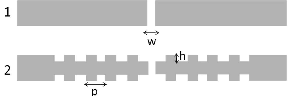
For directional beaming measurements we designed two structures: 1) the reference sample (a metal plate with a subwavelength slit in it), 2) a subwavelength slit surrounded by periodic gratings as shown in Fig. 2.3. These samples were metallic and made of aluminum (Al). The samples were fabricated using a CNC machine with a process resolution of 0.1 mm. Slit width was 2 mm. Metal thickness is defined as the thickness that light passes through, which is 8 mm. Period of the grating was 16 mm, groove depth was 4 mm.
Figure 2.3: (a) The reference sample (a metal plate with a subwavelength slit in it), (b) a subwavelength slit surrounded by periodic gratings where w=2 mm, h=4 mm and p= 16 mm.
According to the coupling formula:
(2.2)
where k
g=2π/λg, period of the grating is important in coupling. It should not be greater or smaller than our study range (8mm-30mm). We chose 16 mm for grating periodicity (λ
g). According to the previous studies by grating structures [41] deeper groove depths (h) for grating produce better results.
CHAPTER 2. OFF-AXIS BEAMING FROM METALLIC GRATINGS 11
2.3.1. Simulation
Theoretical calculations were done using the finite-difference-time-domain (FDTD) method-based simulations. FDTD is a direct space-time approach. The basic algorithm of FDTD method depends on Maxwell’s equations. When Maxwell's differential form equations are examined, it can be seen that the time derivative of the E field is dependent on the Curl of the H field. Thus, the change in the E field (the time derivative) is dependent on the change in the H field across space (the Curl). This results in the basic FDTD equation that the new value of the E field is dependent on the old value of the E field (hence the difference in time) and the difference in the old value of the H field on either side of the E field point in space. The H field is found in the same manner. The new value of the H field is dependent on the old value of the H field (hence the difference in time), as well as dependent on the difference in the E field on either side of the H field point.
In this method, an oscillating wave source is introduced into the grid and “directed” at the structure to be analyzed. The entire grid is then time-stepped until steady state response oscillations are obtained at all points on the grid. In order to use FDTD, a computational domain where the simulation will be performed must be established. The E and H fields will be determined at every point within the computational domain. The material (air, metal or dielectric) of each cell within the computational domain must be specified. Once the computational domain and the grid material are established, a source is specified. It is suitable to introduce a Gaussian pulse, to calculate the spectral response.
Since the E and H fields are determined directly, the output of the simulation is usually the E or H field at a point or a series of points within the computational domain.
To define structures, permittivity should be specified. Permittivity of free-space (air) is 1. The permittivity of metal depends on the frequency of the incident radiation. So, we modeled our structure by using the Drude dispersion model,
CHAPTER 2. OFF-AXIS BEAMING FROM METALLIC GRATINGS 12
which is one of the models to determine the frequency dependent permittivity of metals. Drude model assumes that, all of the conduction electrons can freely move around inside the metal to form a gas of non-interacting particles. The permittivity is given by the relation:
(2.3) where ωp=3570 THz is the plasma frequency, and ωτ=19.4 THz is the absorption
coefficient for aluminum [42].
CHAPTER 2. OFF-AXIS BEAMING FROM METALLIC GRATINGS 13
2.3.2. Measurements
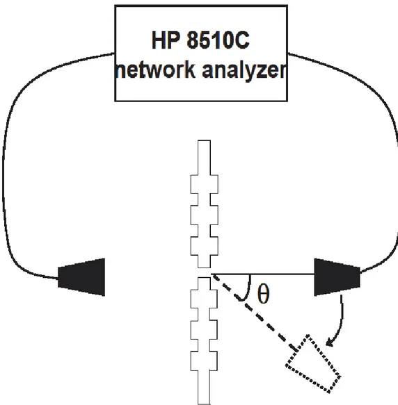
The experimental setup consisted of an HP 8510C network analyzer and two standard gain horn antennae in order to measure the transmission amplitude. Radiation was normally incident upon the sample from 15 cm by a source antenna. The receiver antenna was 100 cm away from the sample (Fig. 2.4). The receiver antenna is connected to a rotating arm to measure the angular dependence of the radiation. We change the angle of the receiver antenna with the help of rotating arm. We have 10 resolution in this experimental setup. Measurements were performed in the microwave spectrum of 10-18 GHz, corresponding to a wavelength region of 16.7-30 mm. Both transmitter and receiver antennas were in TM mode, so that the electric field was perpendicular to the groove direction.
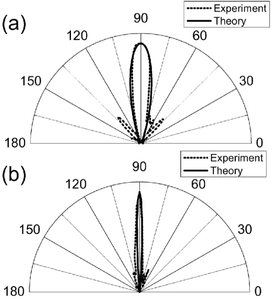
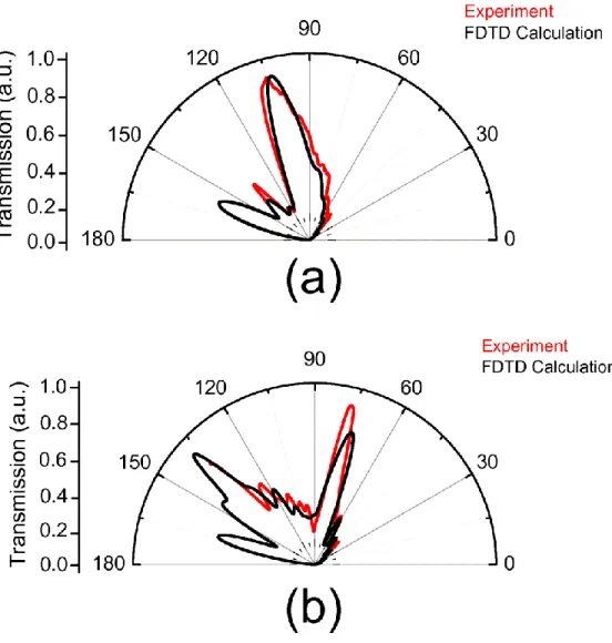
Figure 2.5 presents the normalized measured and calculated angular transmission distribution at the resonance frequency (14 GHz) for reference sample and slit surrounded by periodic gratings. Angular divergence of the transmitted beam from reference sample is ±12o, whereas the transmitted beam that emerges from slit surrounded by periodic gratings is ±3o. The angular divergence of the beam reduced four times.
CHAPTER 2. OFF-AXIS BEAMING FROM METALLIC GRATINGS 14
Figure 2.5: The normalized measured and calculated angular transmission distribution at the resonance frequency (14 GHz) in linear scale for (a) reference sample and (b) slit surrounded by periodic gratings.
CHAPTER 2. OFF-AXIS BEAMING FROM METALLIC GRATINGS 15
2.4. Off-axis beaming
The emitted EM waves are confined to a narrow spatial region when the exit surface of the subwavelength aperture was surrounded by periodic gratings since the surface-wave momentum and the momentum of the corrugation around the subwavelength aperture limit the allowed range of momentum of the reradiated EM waves.
The beam is directed on the axis of the propagation direction, if the subwavelength aperture has symmetric grating periods on different sides of the output surface [15-17, 43]. However, it is possible to steer the beaming angle by using asymmetric grating periods. In order to optimize the grating periods, we firstly investigated the structures with gratings only on one side. The structures used in this study are shown in Fig.2.6.
Figure 2.6: The structures used in this work where a=7 mm, b=8 mm, c=11 mm, and t=16 mm. The slit widths were 2 mm and the grating heights were 4 mm. All of them have the same input surface grating period of 16 mm in order to couple the SPs.
CHAPTER 2. OFF-AXIS BEAMING FROM METALLIC GRATINGS 16
Figure 2.7: The beaming angle is steered for structures with grating periods only on one side of the output surface. The beam is mostly directed to the negative side for (a) Sample 1 and positive side for (b) Sample 2 at 14.5 GHz (20.7 mm).
We calculated the angular distribution of the transmission for a structure with a grating period 14 mm on one side of the output surface (Sample 1). In the simulation, an EM wave with an E field that was polarized in the x direction is
CHAPTER 2. OFF-AXIS BEAMING FROM METALLIC GRATINGS 17
incident from the bottom. After the field passes through the aperture, it emits in the +z direction. The EM waves throughout Sample 1 are mostly directed to the negative side (we defined the right side of the 90o as positive and the left side as negative) at 14.5 GHz (Fig. 2.7 (a)).
Although the EM waves throughout Sample 1 were mostly directed towards -15o, the beam was not collimated to the narrow range. In order to obtain off-axis directional beaming we need to arrange the other side of the sample with a period that is different than 14 mm. We optimized this period by FDTD calculations to where the structure emits EM waves to the positive side. The calculated transmission for structure with a grating period 22 mm (Sample 2) shows that most of the emitted EM waves were directed towards the positive side. In the measurements of our second sample, we observed a beam at 15o on the positive side (Fig. 2.7(b)). This case is the exact opposite of Sample1.
It is possible to steer the beam by only using Sample 1 or 2. However, the beaming is not as clear for them. In order to obtain off-axis as well as directional beaming, we combined these two structures (Sample 3). The combination of these gratings will provide a directional yet off-axis beam through the positive side. The calculated transmission between 10-20 GHz from Sample 3 shows that at the SP resonance frequency (14.5 GHz) the emitted EM waves were directed towards the positive side (Fig. 2.8).
CHAPTER 2. OFF-AXIS BEAMING FROM METALLIC GRATINGS 18
Figure 2.8: The calculated transmission throughout Sample 3 shows that off-axis and directional beaming is possible by using metallic asymmetric gratings on the output surface at SP resonance (14.5 GHz).
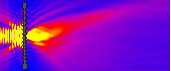
Meanwhile, we measured the angular distribution of the EM waves that were transmitted through Sample 3 with asymmetric grating periods on different sides. We observed off-axis directional beaming with a beaming angle of 15 degrees and a FWHM (Full-Width Half-Maximum) of 10 degrees (Fig. 2.9). This result is in good agreement with the FDTD calculations. We have also presented the FDTD mode pattern showing the coupling between the top and bottom surface at the resonance frequency (Fig. 2.10).
CHAPTER 2. OFF-AXIS BEAMING FROM METALLIC GRATINGS 19
Figure 2.9: By use of a metallic structure with a subwavelength aperture at the center and the grating periods of 14 mm and 22 mm on the different sides of the output surface, we observed off-axis directional beaming with an FWHM of 10o and the beaming angle of 15o. It is possible to steer the beaming angle by arranging the grating periods of the output surface of the metallic structure.
Figure 2.10: FDTD mode pattern showing the coupling between the top and bottom surface at the resonance frequency.
CHAPTER 2. OFF-AXIS BEAMING FROM METALLIC GRATINGS 20
2.4.1. Origin of the off-axis beaming
When a p-polarized EM wave, which is incident to the metallic surface induced surface waves, flows though the aperture, and via grating, diffraction beaming phenomena occur. The SP dispersion relation and grating equation states that:
(2.4)
where ksp is the wave vector of SP, ko// is the portion of the incident wave vector
that is in the plane of the metal, N is an integer, and kg = 2π/λg is the grating wave
vector where λg is the grating period.
The possibility to have steered beaming is a combinatory result of the generalized form for the conservation of the parallel component of the wave vector at the interface of a periodic medium, and the finite angle span of the source. Finite width sources can never be perfectly collimated. Thus, the input beam has a small
angular span that gives , which is small yet non-zero. The existence
of this small is necessary to obtain the steered beaming phenomenon. This is because, that if , it would be impossible to satisfy
. At the interface of a homogeneous medium the parallel
component of the wave vector is conserved ( ). At the interface of a
periodic medium the parallel component of the wave vector is conserved within a reciprocal lattice vector corresponding to the periodicity of the surface (
). The demonstrated steered beaming (beaming angle different than zero) is always an umklapp process, i.e. a process with, and in particular an umklapp process with N=±1. The beaming angle would be restricted by the angle span of the source.
CHAPTER 2. OFF-AXIS BEAMING FROM METALLIC GRATINGS 21
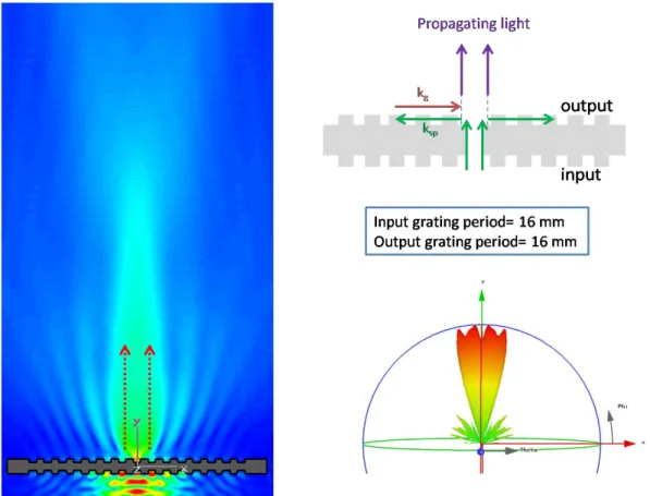
In order to understand the origin of the off-axis beaming we first revisited the symmetric case. The grating vector kg is equal to ksp. Therefore, the projected
direction of the diffracted beam is on-axis (Fig. 2.11). The subwavelength aperture has an input and output side grating period of 16 mm.
Figure 2.11: Calculated E-field and far field for subwavelength apertures with an input and output side grating period of 16 mm.
Hence, we investigate 3 different cases: 1) When the grating vector kg is
larger than ksp, the in-plane component ko// is negative. Therefore, the projected
direction of the diffracted beam is toward the waveguide channel (Fig. 2.12). The subwavelength aperture has an input side grating period of 16 mm and an output surface grating period of 14 mm.
CHAPTER 2. OFF-AXIS BEAMING FROM METALLIC GRATINGS 22
Figure 2.12: Calculated E-field and far field for subwavelength apertures with an input side grating period of 16 mm. The projected direction of the diffracted beam is toward the waveguide channel for a structure with an output surface grating period of 14 mm.
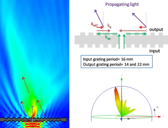
In the second case, the grating vector kg is smaller than ksp, the in-plane
component ko// is positive. Therefore, the projected direction of the diffracted beam
is away from the waveguide channel (Fig. 2.13). The subwavelength aperture has an input side grating period of 16 mm and an output surface grating period of 22 mm.
CHAPTER 2. OFF-AXIS BEAMING FROM METALLIC GRATINGS 23
Figure 2.13: Calculated E-field and far field for subwavelength apertures with an input side grating period of 16 mm. The projected direction of the diffracted beam is away from the waveguide channel for a structure with an output surface grating period of 22 mm.
In the last case, we combined first two cases and obtained and asymmetric grating structure. The combinations of these grating vectors on the different sides of the subwavelength aperture will posses off-axis beaming (Fig. 2.14).
CHAPTER 2. OFF-AXIS BEAMING FROM METALLIC GRATINGS 24
Figure 2.14: Calculated E-field and far field for subwavelength apertures with an input side grating period of 16 mm. The off-axis beam was achieved with the combination of these structures (output surface grating is 14 mm and 22 mm on the different sides of the aperture).
Hence, it is possible to change the beam by using subwavelength metallic apertures via coupling to the surface waves. The gratings have to be arranged asymmetrically in order to steer the beam. We observed a beaming angle of 15 degrees with a FWHM of 10 degrees. The momentum of the periodic corrugation, surface waves and the angle span of the finite source define the beaming angle. Our results show that it is possible to steer beam by the appropriate modification of the output surface.
Chapter 3
3
Off-Axis directional beaming via
photonic crystal surface modes
3.1. Introduction
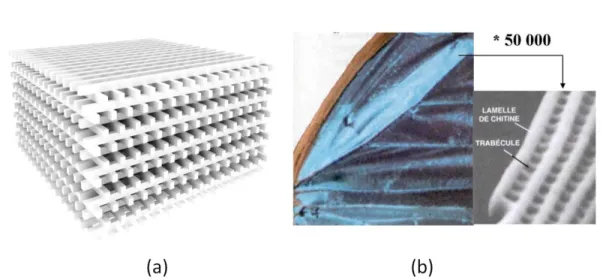
Photonic crystals (PCs) are periodic structures that are designed to affect the motion of photons in a similar way that periodicity of a semiconductor crystal affects the motion of electrons. PCs occur in nature and in various forms have been studied scientifically for the last 100 years. Examples of PC are shown in Fig. 3.1.
For electrons the periodic potential is provided by the periodically arranged atoms in a crystal. We shall note that appearance of a band gap for electrons is a consequence of the periodic potential. Band gap for electrons does not arise from the electron-electron interactions; rather it arises from the electron-lattice periodic potential interaction. Since the existence of a band gap is a consequence of the periodic potential it is natural to ask whether there may be band gaps for the EM waves. The possibility of the existence of band gaps for photons was long ago predicted, as early as 1979 [44]. In the case of photons, the periodic potential is provided by a periodically arranged dielectric constant. In fact the similarities
CHAPTER 3.OFF-AXIS BEAMING VIA PC 26
between the Maxwell equations written in an eigenvalue form and the hamiltonian for an electron propagating in a periodic potential is striking [1].
Figure 3.1: (a) A 3 dimensional PC made from alumina rods. Alumina rods are arranged in a face cubic centered arrangement. (b) There is no pigment in a
butterfly wing which is blue due to PC
(http://www.lpn.cnrs.fr/en/GOSS/CPOI.php).
Along with the existence of a band gap, a periodic potential for photons PCs strongly modify the dispersion properties of EM waves. Since PCs may control the propagation of EM waves in certain directions, they have recently attracted much attention. Many interesting phenomena such as enhancement and suppression of spontaneous emission [45], propagation of photons via hopping over coupled defects [46], and localized donor and acceptor modes [47], have been suggested and observed. One particular application of PCs has been commercialized by Samsung to increase the extraction efficiency of light emitting dioes (LEDs) [48].
A metallic surface and the surface of a corrugated PC have a similar property, i.e., both surfaces can support surface propagating EM waves [49, 50]. In
CHAPTER 3.OFF-AXIS BEAMING VIA PC 27
the previous chapter, we investigated off-axis beaming from an asymmetric metallic surface.
In this chapter, we theoretically show that PC surface can support surface propagating EM waves in the presence of a periodic corrugation. We experimentally demonstrate that when a periodic corrugation is added to the output surface of the PC, the power emitted through the PC waveguide is confined to a narrow angular region. In addition, we investigate theoretically and experimentally the possibility of off-axis beaming from PC waveguide using asymmetric periodic surface layer.
3.2. Surface Propagating Modes of PCs
There are three types of modes that are supported by a finite size PC, which is finite in one dimension and infinitely periodic in the other dimension. The first of these modes extends in the air and PC. The second mode extends in the air but decays in the PC and the last mode decays in the air but extends in the PC. Only the modes that are extending both in air and PC are observed in the transmission spectrum. The intensity profiles of these modes which are calculated using plane wave expansion method have been shown in Fig. 3.2 (a)-(c).
CHAPTER 3.OFF-AXIS BEAMING VIA PC 28
Figure 3.2: Electric field intensity profiles of the modes supported by the finite size PC: (a) mode decays in the air but extends in the PC, (b) mode extends in the air but decays in the PC and (c) mode extends in the air and the PC. (d) Surface mode: decays both in the air and PC; it is localized at the modified interface layer. These field profiles are calculated by using the plane wave expansion method.
On the other hand, the PC can also support one more mode by modifying the PC-air interface. The corrugation may be achieved by reducing the rod radius at the surface of the PC or by using rods of different shape. For this study we changed the radius of the rods at the surface of the PC from 1.55 mm to 0.76 mm.
Modes of an infinite PC can be calculated by using the plane-wave expansion method [51]. The same method can be used to identify the modes of a finite PC by employing a large enough supercell [52]. The PC is a 2 dimensional square array of circular alumina rods. The crystal is assumed to be continuous along z axis in our band structure calculations. The radius of the rods is 1.55 mm. The dielectric constant of alumina is 9.61. Lattice constants along x and y directions are 11 mm. The supercell is 40 layers long along y axis and consists of 1 unit cell along x axis. 15 unit cells along y axis contain alumina rods and the rest is free space. For comparison, we calculated the band structure of an infinite PC, i.e., infinite both in x axis and y axis (Fig 3.3(a)).
CHAPTER 3.OFF-AXIS BEAMING VIA PC 29
The band structure of the finite PC is calculated by plane wave expansion method with a large supercell is shown in Fig. 3.3 (b). Figure 3.3(c) shows that when the corrugation is added a band below the light line appears in the band structure (This band is shown with blue solid line in Fig. 3.3 (c) and (d).) This band is inside the photonic band gap and extends from 11.9 GHz to 12.8 GHz. The electric field intensity corresponding to these modes is calculated and plotted in Fig. 3.2 (d). Figure 3.2 (d) shows that the electric field intensity for these modes is evanescent both in air and inside PC. However, these modes have real wave vectors parallel to the PC surface. As a result, these modes are surface propagating waves.
Figure 3.3: (a) The TM (electric field parallel to the axis of the rods) band structure of the infinite size PC (b) the TM band structure of the finite size (c) the TM band structure of the finite size PC when the radius of the rods at the surface of the PC is reduced to 0.76 mm. (d) zoomed view of the TM band structure of the finite size PC when the radius of the rods at the surface of the PC is reduced to 0.76 mm.