DESIGN AND IMPLEMENTATION OF A 0.6
GHz-0.9 GHz RF-SQUID READ-OUT SYSTEM AND
INVESTIGATION OF RF-SQUID SIGNAL
CHARACTERISTICS
A THESIS
SUBMITTED TO THE DEPARTMENT OF ELECTRICAL AND ELECTRONICS ENGINEERING
AND THE INSTITUTE OF ENGINEERING AND SCIENCE OF BILKENT UNIVERSITY
IN PARTIAL FULFILLMENT OF THE REQUIREMENTS FOR THE DEGREE OF
MASTER OF SCIENCE
By Taylan EKER
I certify that I have read this thesis and that in my opinion it is fully adequate, in scope and inquality, as a thesis for the degree of Master of Science.
Assist. Prof. Dr. Mehdi Fardmanesh (Supervisor)
I certify that I have read this thesis and that in my opinion it is fully adequate, in scope and inquality, as a thesis for the degree of Master of Science.
Assoc. Prof. Dr. Iman Askerzade
I certify that I have read this thesis and that in my opinion it is fully adequate, in scope and inquality, as a thesis for the degree of Master of Science.
Prof. Dr. Ziya Ider
Approved for the Institute of Engineering and Science:
Prof. Dr. Mehmet Baray
ABSTRACT
DESIGN AND IMPLEMENTATION OF A 0.6 GHz -
0.9 GHz RF-SQUID READ-OUT SYSTEM AND
INVESTIGATION OF RF-SQUID SIGNAL
CHARACTERISTICS
Taylan EKER
M. S. in Electrical and Electronics Engineering Supervisor: Assist. Prof. Dr. Mehdi Fardmanesh
June 2005
Design and implementation of a transceiver system for rf-SQUID (Superconducting Quantum Interference Device) operation is investigated in this work. Besides, experiments to characterize the rf-SQUID have been performed using the implemented system.
The steps in system design and implementation are presented. The difficulties and drawbacks of the system are reported and alternative techniques required to overcome these problems are determined. Also, for the operation of the rf-SQUID at much higher frequencies, different transceiver architecture is proposed and possible drawbacks are stated.
Using implemented system, several experiments were performed on two high Tc
rf-SQUID gradiometers with a tank-circuit resonating at 720 MHz. In these experiments, the frequency and amplitude of the applied rf signal were swept and output flux to voltage transfer signal (modulation added by rf-SQUID), Vspp, and incoming rf signal
ÖZET
0.6 GHz - 0.9 GHz FREKANS BANDINDA ÇALISAN
RF-SQUID ÖLÇÜM SISTEMININ TASARIMI VE
GERÇEKLENMESI, VE RF-SQUID SINYAL
ÖZELLIKLERININ ARASTIRILMASI
Taylan EKER
Elektrik ve Elektronik Mühendisligi Bölümü Yüksek Lisans Tez Yöneticisi: Yrd. Doç. Dr. Mehdi Fardmanesh
Haziran 2005
Rf-SQUID (Üstüniletken Kuantum Girisim Cihazi) çalismasi için bir verici-alici sistemi tasarlanip gerçeklenmistir. Bunun yani sira, gerçeklenen sistem kullanilarak, rf-SQUID tanimlamasina yönelik deneyler yapilmistir.
Sistemin tasarimi ve gerçeklenmesinde izlenen adimlar sunulmustur. Sistemde karsilasilan zorluklar ve dezavantajlar raporlanmis ve bu problemlerin asilmasi için gereken baska tekniklere belirlenmistir. Ayrica, rf-SQUID’in daha yüksek frekanslarda çalismasi için farkli bir verici-alici mimarisi önerilmis ve olasi dezavantajlar belirtilmistir.
Gerçeklenen sistem kullanilarak, 720 MHz frekansinda tinlayan bir depo devresiyle iki yüksek kritik sicaklikli rf-SQUID meyilölçer üzerinde çesitli deneyler yapildi. Bu deneylerde, uygulanan rf isaretin genlik ve frekansi kaydirilmis, çikista alinan Vspp
(rf-SQUID tarafindan eklenen modülasyon) ve gelen rf isaretin tayfi raporlanip incelenmistir.
Acknowledgement
I would like to express my sincere gratitude to Dr. Mehdi Fardmanesh for his supervision, guidance, suggestions, and encouragement throughout my graduate study.
I would also like to thank my graduate committee members, Assoc. Prof. Dr. Iman Askerzade and Prof. Ziya Ider for reading and commenting on the thesis.
I would like to express my endless thanks to Ali Bozbey and Rizwan Akram for sharing their experiences with me and their essential help in performing the SQUID signal measurements. Also, I am thankful to my colleagues in Aselsan for their help.
Finally, I am so thankful to my wife, my parents and sisters, and my wife’s family for their support.
Contents
1 INTRODUCTION AND LITERATURE SURVEY ...1
1.1 Introduction...1
1.2 Briefly Superconductivity...2
1.3 SQUID ...4
1.3.1 Josephson Junction...5
1.3.2 SQUID Types...8
1.4 Conventional Read-Out Electronics ...17
2 DESIGN AND IMPLEMENTATION OF AN EXPERIMENTAL RF-SQUID READ-OUT SYSTEM ...20
2.1 RF-SQUID Functioning...20
2.2 Tank Circuit Assembly ...27
2.3 RF Subsystems Design ...32
2.3.1 Transmitter (Tx) ...33
2.3.2 Receiver (Rx) ...35
2.3.3 Flux Feeding ...45
2.4 Implementation of rf-SQUID Read-Out System ...45
2.4.2 Practical Issues in Implementation ...63
2.4.3 Implemented System and Sample Measurements...66
3 EXPERIMENTS AND RESULTS ...69
3.1 Preliminary Work and Device Settings...69
3.2 Rf-SQUID Output Response (Vspp) and Spectrum Measurements ...72
4 CONCLUSIONS AND FUTURE WORK ...83
APPENDIX A ...85
A.1 Power Conversions ...85
A.2 Device and Instrument Information...86
A.3 Abbreviations ...104 CONTENTS
List of Figures
1.1 Critical temperature of various superconductors on years base………4
1.2 The Josephson Junction ...5
1.3 dc-SQUID and its equivalent schematic view ...9
1.4 Voltage created in SQUID tank circuit versus applied current for changing flux bias ...10
1.5 Output voltage of dc-SQUID for changing applied magnetic field ...10
1.6 rf-SQUID and its equivalent schematic view ...12
1.7 Total flux vs applied flux for different hysteresis parameter values ...15
1.8 Total flux versus applied flux for a superconducting ring ...16
1.9 A typical schematic for rf-SQUID readout electronics...17
2.1 A set- up to understand the response of rf-SQUID to an applied rf-pump ...21
2.2 The envelope of SQUID response ...22
2.3 Staircase pattern for different DC biases ...23
2.4 The effect of externally applied low frequency signal flux together with rf power flux ...25
2.5 Envelope of the response of rf-SQUID vs. applied flux in second mode of
operation for different initial biasing conditions, B1 and B2. ...25
2.6 A typical plot of implemented system ...26
2.7 Utilized tank circuit topology ...28
2.8 A typical plot of tank circuit S11 ...31
2.9 Transmitter Subsystem...33
2.10 Rf power spectrum for 720 MHz frequency at the output of two channels of the transmitter subsystem...35
2.11 Receiver, Schematic View ...36
2.12 Intercept Point Definition and IP3 ...44
2.13 Amplifier S11 and S21...46
2.14 Amplifier S22 and S12...47
2.15 1dB compression point of the amplifier...48
2.16 Gain decrease for the exact measurement of 1dB compression...48
2.17 IP2 measurement...49
2.18 IP3 measurement...49
2.19 S parameter measurement of an attenuator...50
2.20 S11 and S21 of the coupler ...51
2.21 Isolation parameter of the coupler ...51
2.22 S11 and S21 related to designed power divider ...52
2.23 Isolation parameter of power divider...53 LIST OF FIGURES
2.25 S21 of the filter ...54
2.26 10 inch cable S-parameters ...55
2.27 Established Setup to measure mixer ...56
2.28 Tank circuit assembly setup ...58
2.29 Tank Circuit S11 ...59
2.30 S-parameters of the receiver ...60
2.31 1 dB Compression Point of Receiver ...61
2.32 Transmitter LO arm S-parameters ...62
2.33 Transmitter SQUID arm S-parameters ...62
2.34 A picture of receiver system ...64
2.35 A picture of transmitter system...65
2.36 Tank Circuit Assembly ...66
2.37 Implemented System...67
2.38 Measurement of applied flux and SQUID response on TDS 2024 oscilloscope in Y-T mode ...68
2.39 Measurement of applied flux and SQUID response on TDS 2024 in X-Y mode...68
3.1 A program written in labview to automate measurements ...70
3.2 3D plot of rf-SQUID peak to peak response for changing frequency and rf pump amplitude-SQUID1 ...72
3.3 Contour plot of rf-SQUID peak to peak response for changing frequency and rf pump amplitude-SQUID1 ...73 LIST OF FIGURES
3.4 Grayscale profile plot of rf-SQUID peak to peak response for changing frequency
and rf pump amplitude.-SQUID1 ...73
3.5 3D plot of rf-SQUID peak to peak response for changing frequency and rf pump amplitude-SQUID2 ...74
3.6 Contour plot of rf-SQUID peak to peak response for changing frequency and rf pump amplitude-SQUID2 ...74
3.7 Grayscale profile plot of rf-SQUID peak to peak response for changing frequency and rf pump amplitude.-SQUID2 ...75
3.8 SQUID1 Vspp measurement with 15dB attenuation...76
3.9 SQUID1 spectrum measurement ...76
3.10 Spectrum and Vspp measurement for SQUID1 with 15 dB attenuation level ...77
3.11 SQUID2 Vspp measurement with 15dB attenuation...78
3.12 SQUID2 spectrum measurement ...78
3.13 SQUID1 Vspp measurement with 5 dB attenuation...79
3.14 SQUID1 spectrum measurement ...80
3.15 SQUID2 Vspp measurement with 5 dB attenuation...81
3.16 SQUID2 spectrum measurement ...81
A.1 Outline Drawing of SCA-4 Amplifier ...87
A.2 Biasing configuration of SCA-4 ...88
A.3 Outline Drawing of ZFM-2H...89
A.4 Functional Schematic and Pin Assignments of AT20-0263 ...94
A.5 Package Dimensions ...95 LIST OF FIGURES
A.6 600MHz - 900MHz Filter Schematic View ...96 A.7 Schematic view of power divider...97 A.8 Outline Drawing of JTOS-1025...99 LIST OF FIGURES
List of Tables
2.1 Amplifier Properties...37
2.2 Filter Characteristics ...37
2.3 Mixer properties ...38
2.4 Noise and Power in each stage of the receiver system ...40
2.5 Assumptions for calculations ...40
2.6 Results characterizing the receiver ...41
2.7 Power measurements of amplifier...49
2.8 The spectrum at the if port of mixer after a sample mixing action...57
2.9 Devices and subsystems used in the setup ...67
3.1 Signal Generator Settings ...71
3.2 Spectrum Analyzer Settings...71
A.1 Conversion between power conventions and voltage for Z0=50 ...85
A.2 Electrical Specifications ...86
A.3 Pin Arrangement ...88
A.6 Typical Performance Data - 1 ...91
A.7 Performance Data-2 ...92
A.8 Electrical Specifications of AT20-0263...93
A.9 Truth Table...94
A.10 Specifications of JTOS 1025 ...98
A.11 Pin Assignments...99
A.12 Dimensions ...99
A.13 Performance Data 1...100
A.14 Performance Data 2...101
A.15 Phase Noise ...101
A.16 Electrical Specifications for Minibend cables ...103
A.17 Abbreviations and their meanings ...104 LIST OF TABLES
Chapter 1
INTRODUCTION AND LITERATURE SURVEY
1.1 Introduction
Superconductivity phenomenon was discovered in very early 20th century. Before the discovery of superconductivity, the gradual decrease in the resistance of a cooled material had been known. After the success in liquefying helium and reaching temperatures below 4.2 K, several materials were found that showed a sharp drop in their resistance, going to the superconducting state later at some temperature, called the critical temperature, Tc. After the discovery of superconducting materials with higher
critical temperatures, a new area was opened in the field. Besides, with the discovery of superconductivity, several theories about the principles of superconductivity mechanism were established [1].
Superconductivity is used in a variety of applications including power lines and cables, magnetic levitation trains, detection systems, microwave, biomedical systems, etc [1]. In this study, the focus is on Superconducting Quantum Interference Devices (SQUIDs) made of high temperature class of superconductors (detection systems).
SQUIDs are extremely sensitive magnetic flux detectors. The operation of them is based on the modulation created on the applied current caused by an externally applied
flux. They cover a wide range of applications such as biomagnetic systems, geophysics, commercial systems for measurement of magnetic properties of materials and non-destructive evaluation (NDE) of materials and electronic warfare [1], [2].
In this work, an experimental read-out system for rf-SQUIDs is designed and implemented. Following implementation of the system, several experiments are performed to investigate characteristics of rf-SQUID for different frequencies and amplitude levels. While explaining these works, several references are inserted for interested readers.
This thesis has three main parts. In the first part (LITERATURE SURVEY), background information about the basics of SQUID operation and the principles of typical read-out electronics are introduced. Second part (DESIGN AND IMPLEMENTATION OF AN EXPERIMENTAL RF-SQUID READ-OUT SYSTEM) contains the design and implementation of an rf-SQUID read-out system in details for each subsystem block. The third part (EXPERIMENTS AND RESULTS) consists of the experiments performed to characterize some rf-SQUIDs and the results.
Chapter 5 (CONCLUSIONS AND FUTURE WORK) describes the works to be done in the future to improve the performance of the implemented system and the strategy to be taken for higher frequency read-out systems.
1.2 Briefly Superconductivity
Superconductivity is a phenomenon displayed by some materials below a critical temperature, Tc. At this condition (below Tc), superconductors exhibit zero dc electrical
resistance and perfect diamagnetism [1]. A very important characteristic of
namely Josephson Junctions. The Josephson Junctions are the base of the very valuable devices such as super-sensitive magnetic sensors, SQUIDs (Superconductive Quantum Interference Devices), which are the base devices in this work and further studied in the following sections.
For years, several scientists put forward various theories about superconductivity, some of which are London Theory, Ginzburg Landau Theory, and the BCS theory (first letters of Bardeen, Cooper, and Schrieffer, who have modeled Type I superconductors). Of listed theories, the BCS theory greatly attracted attention of superconductivity societies. The BCS theory is out of the scope of this report and more information about it and other theories can be found in [4]-[8]. Superconductor materials can be grouped into two types, namely type I and type II superconductors. Characteristically, type I superconductors totally exclude magnetic fields below their Tc. If the applied magnetic
field is of low amplitude, Type II superconductors can exclude it but they can only partially exclude high amplitude magnetic fields [1]. Interested readers may refer to [4]-[5] for more information on Type I and Type II superconductor properties and characteristics.
Another classification of superconductors can be made upon the critical temperature they exhibit. By 1973, metallic alloys having critical temperatures up to 23 K were found [4]. In 1986, Bernorz and Müller [6] showed the possibility of copper oxides to have higher critical temperatures (35 K). After this point, new materials having critical temperatures up to 136 K were found. As a result, superconductors with critical temperatures below 23 K are typically low-temperature superconductors (LTS), and that with critical temperatures above 23K are mostly high temperature superconductors (HTS) [4]. In Figure 1.1, critical temperatures of some superconductors are shown [4]. The study of this work is focused on HTS devices made of YBa2CO3O7-x material.
Figure 1.1 Critical temperature of various superconductors on years base
1.3 SQUID
SQUID is a sensitive flux to voltage transducer and has the sensitivity that makes it popular among all magnetic sensors. Main properties of SQUIDs include extremely high sensitivity (down to a few fT/Hz-1/2), wide bandwidth (DC – 10kHz), broad dynamic range (>80dB), and quantative nature in terms of intercepted magnetic field [10]. These properties of SQUIDs allow engineers to design and implement efficient detectors working on wider bandwidths with higher dynamic ranges.
The principles of SQUIDs are based on the Josephson Junctions, which is reviewed CHAPTER 1. INTRODUCTION AND LITERATURE SURVEY
1.3.1 Josephson Junction
Josephson Junctions are primary for the understanding of SQUIDs. Mainly, two superconductors having insulating barrier in between form a Josephson Junction. There are different types of Josephson Junctions such as S-N-S (Superconductor-Normal Conductor-Superconductor) and S-I-S (Superconductor-Insulator-Superconductor). In Figure 1.2, a basic figure of Josephson junction is shown. In this figure, sides 1 and 2 are superconductors, which are intercepted by an insulator (S-I-S).
Figure 1.2 The Josephson Junction
The superconductivity wave function characterizing the condensed electron pairs (cooper pairs) assuming large separation between superconductors, can be defined as [4]; ( )
{
( 2 / )}
( )
i r f h tr
e
θ εψ
=
ψ
r
− (1.1)where ψ
( )
r is square root of cooper pair density and θ( )
r is the phase of the wave function of cooper pairs. For the two sides of the junction, the wave function of cooper CHAPTER 1. INTRODUCTION AND LITERATURE SURVEYpairs has unlocked phases. Reduction of separation between the superconductors leads to penetration of ψ into the barrier and thus phases become locked (no energy reduction during cooper pair transition). An applied voltage can also accomplish pair tunneling. In this case, the phases are uncorrelated again, but the phase difference between the junctions evolves as a function of the applied voltage [3], [4].
Time evolution of wave functions for two sides of the junction can be described by,
1 1 1 2 2 2 2 1 i U K t i U K t ψ ψ ψ ψ ψ ψ ∂ = + ∂ ∂ = + ∂ h h (1.2)
In this equation, ψ is the wave function of pairs on side 1 and 1 ψ is the wave function 2 for side 2. U and 1 U are the energies of the wave functions on side 1 and side 2, 2 respectively and, K is the coupling coefficient between the wave functions. It is assumed that a voltage (V) is applied on the junction and an energy difference of U2 −U1 is created between two sides of the junction. If the energies of the wave functions in the middle of the insulator is assumed to be zero, equation 1.2 becomes,
* 1 1 2 * 2 2 1 2 2 e V i K t e V i K t ψ ψ ψ ψ ψ ψ ∂ = − + ∂ ∂ = + ∂ h h (1.3)
Besides, the wave functions at two sides of the insulator can be expressed by the
electron pair densities,
( )
1 * 2 i k k
n
ske
θ
ψ
=
. Also, the phase difference between the twosides of the junction can be introduced as δ θ θ= −2 1. In the light of these equations, equation 1.3 can be reinterpreted as (by separating real and imaginary parts) [4]
1 * * * 1 2 1 2 2 ( ) sin s s s n K n n t δ ∂ = ∂ h (1.4) 1 * * * 2 2 1 2 2 ( ) sin s s s n K n n t δ ∂ = − ∂ h (1.5) 1 * 2 * 2 1 * 1 cos 2 s s n K e V t n θ δ ∂ = − + ∂ h h (1.6) 1 * 2 * 1 2 * 2 cos 2 s s n K e V t n θ δ ∂ = − − ∂ h h (1.7)
According to equations 1.4 and 1.5, there is a tendency of rate of change in pair densities in both sides of the junctions. This tendency is opposite for each side of the junction. This tendency is balanced by the current that flows through the circuit, which connects two junctions. If the phase gradient from side 1 to side 2 is positive, i.e. δ >0, the current density from side 2 to side 1 becomes positive. Thus, there should be transfer
of electrons from side 1 to side 2 ( * *
1 0 , 2 0
s s
n n
t t
∂ < ∂ >
∂ ∂ ). This requires the coupling to be
negative.
According to equation 1.4, the current density through the junction is,
sin
c
J =J δ (1.8)
where J is the current density whose derivation is out of the scope of this thesis. Also c
taking the difference between equation 1.6 and 1.7, and equating ns1* and ns2*to each CHAPTER 1. INTRODUCTION AND LITERATURE SURVEY
other, the time derivative of the phase difference between the two sides of the junction can be found. 2e V t δ ∂ = ∂ h (1.9)
In equation 1.9, e* is taken as −2e. Equations 1.8 and 1.9 are the Josephson relations, which express the electron pair behaviors [4], [10].
More details on Josephson Junctions can be found in [4], [5], [10], and [12].
1.3.2 SQUID Types
SQUIDs are fabricated by placing Josephson junctions on super-conducting loops. There are basically two types of SQUIDs which are of interest in this subsection namely rf-SQUID and dc-rf-SQUID. They have different number of Josephson Junctions intercepting their loop as explained in the following parts.
• dc-SQUID
dc-SQUID is formed by a superconducting loop interrupted by two Josephson Junctions. In Figure 1.3, a sample plot of the dc-SQUID and its electrical equivalent schematic is shown.
Figure 1.3: dc-SQUID and its equivalent schematic view
An externally applied magnetic flux creates a phase difference across the junctions where the phase difference is detected as voltage via electronics [4]. The logic in DC-SQUID operation is very similar to the logic in RF-DC-SQUID operation in the sense that the detected voltage is a measure of the phase difference across the junctions.
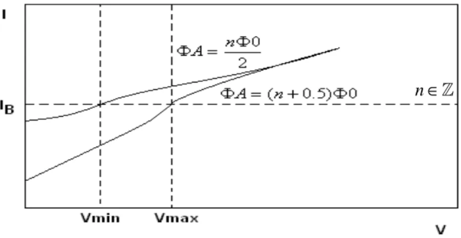
The relation between the induced voltage and applied flux into SQUID at constant bias points is plotted in Figure 1.4. In this figure, y-axis is the applied current on the tank circuit and x-axis is the resulting voltage induced on the tank circuit. Besides, two extreme cases of applied flux on SQUID are plotted in the same figure. According to the figure, a constant current applied to DC-SQUID biases the SQUID at a fixed current on the y-axis. If the externally applied flux (an AC flux) exceeds the flux quanta, which is intercepted by SQUID, the output voltage would be a periodic function between the quanta points. So the output voltage would roughly be a sinusoidal [10] waveform CHAPTER 1. INTRODUCTION AND LITERATURE SURVEY
oscillating between Vmax and Vmin. By changing the current bias, the values of Vmin and
Vmax can be changed; leading to higher signal levels at the output. A sample plot of the
output waveform is shown in Figure 1.5 [10], [4].
Figure 1.4: Voltage created in SQUID tank circuit versus applied current for changing flux.
CHAPTER 1. INTRODUCTION AND LITERATURE SURVEY
n∈¢
According to Figure 1.5, if we bias the SQUID at fixed currents, the SQUID can be in conditions C1, C2, or C3. Assume that the SQUID is biased at point C1. In this condition, the SQUID’s response to the applied flux (can be rf-flux, which is the case in rf-SQUID) of frequency ω would be at frequency of ω again. If the SQUID were biased at point C3, the phase of the response would be reversed at frequency of ω again. Lastly, if the SQUID is biased at point C2, there would be a phase transition of 180 degrees during an ac cycle, so the output voltage would have a frequency of 2ω [10], [12], [13].
More details about the DC-SQUIDs will not be investigated in this report, since it is out of the scope of this thesis. Interested readers can find further information and related equations about DC SQUID in [4], [12], [15], and [16].
• rf-SQUID
rf-SQUID is a superconducting loop similar to DC SQUID, but it is interrupted by only one Josephson Junction. A plot of rf-SQUID and its equivalent electrical schematic is demonstrated in Figure 1.6.
Figure 1.6: rf-SQUID and its equivalent schematic view
As mentioned in section 1.3.1, electron pairs in superconducting state are described by an order parameter, which is similar to a many body wave function.
) ( | ) ( | ) (r ψ r eiθ r ψ = (1.10)
Considering the rf-SQUID shown in Figure 1.6, if we take the integral of the phase of the wave function around the superconducting loop clockwise, and using superposition, it is found that;
∫
2∇ =∫
∇ −∫
∇ 1 1 2 . . . J J J J l d l d l dr θ r θ r θ (1.11)The term on the left side of equation 1.11 is the integral on the loop except the discontinuity. This integral is a multiple of 2π . The first integral on the right side is CHAPTER 1. INTRODUCTION AND LITERATURE SURVEY
taken on the loop including the discontinuity, and it should be the phase difference between the junction edges [4]. The right side of the equation can be adjusted as
2 2 1 0 1 2 2 ( ( )) . J J J J e Adl πΦ θ θ − − − − Φ
∫
r r h (1.12)where the phase gradient is written in terms of vector potential [17]. Then, equation 1.11 becomes [4], [12];
∫
− Φ Φ − = − + − 2 1 0 1 2 . 2 2 ) ( 2 J J J J Adl e n r r h π θ θ π (1.13)Also the gauge invariant phase across the junction is defined as [4];
∫
+ − = 2 1 1 2 . 2 J J J J Adl e r r h θ θ φ (1.14)and equation 1.13 becomes;
0 2 2 Φ Φ − = π π φ n (1.15)
In equation 1.15, Φ is flux inside the loop. If an external field is applied to the SQUID, the flux relation becomes;
LI
ext +
Φ =
Φ (1.16)
where L is the effective inductance of the SQUID loop, and I is the total current flowing through the loop. If we adapt the last equations (1.15 and 1.16) into relevant positions of equation 1.8, the current through the loop becomes [4], [13];
) / 2 sin( − Φ Φ 0 = Ic π I (1.17)
and the total flux inside the loop becomes [13];
) / 2 sin(− Φ Φ0 − Φ = Φ ext LIc π (1.18)
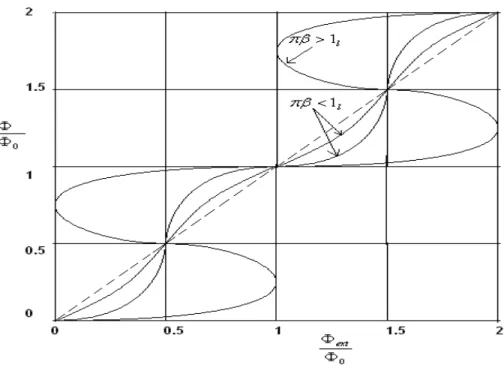
In equation 1.18, an important parameter for the operation of rf-SQUID can be extracted. This parameter is called the hysteresis parameter,πβ , where l β is given by; l
0 2 Φ = c l LI β (1.19)
According to this parameter, rf-SQUID can be hysteretic (πβl >1) or non-hysteretic (πβl <1) [12]. In Figure 1.7, a plot of Φext vs. Φ is shown for different hysteresis parameter values.
Figure 1.7: Total flux vs applied flux for different hysteresis parameter values
According to Figure 1.7, in hysteretic mode, total flux penetrating the rf-SQUID, has a negative slope in the curve as opposed to that in non-hysteretic case. Figure 1.8, taken from [12], shows the same curve in which the loop is closed. To see the effect of discontinuity, those two graphs (Figures 1.7 and 1.8) should be compared to each other. For more information about the theory and applications for SQUID, reader is encouraged to read [28].
Figure 1.8: Total flux versus applied flux for a superconducting ring
Implementation of rf-SQUID (and dc-SQUID) is another area of interest. This subject is out of the scope of this report. Information about techniques and technologies in implementation of SQUIDs can be found in [18]-[22].
1.4 Conventional Read-Out Electronics
Read-out electronics for rf-SQUID is an area in which a hard challenge is going on between different superconductivity groups. The main challenges are
• Decreasing the noise (increasing SNR, so the dynamic range of receivers) contributing from the electronics and the tank circuits.
• Going to higher frequencies together with new resonator topologies. (The characteristics of rf-SQUID should be analyzed in microwave frequencies and various superconductivity groups carry out studies about this. But, at microwave frequencies, conventional tank circuits are not used and instead, resonator topologies for these frequencies are utilized.)
These purposes would inevitably lead to lower noise electronics with higher operating frequencies. Being the main subject of this thesis, the most common topology for the rf-SQUID readout electronics is shown in Figure 1.9, [13].
Figure 1.9: A typical schematic for rf-SQUID readout electronics (The output is Vs)
The system presented in Figure 1.9 is a typical transceiver circuit, but additionally transmitting low frequency signal to modulate the pumped rf power. The rf power is sent and received via a directional coupler. After the detector, the remaining signal is the amplitude modulation that SQUID adds to incoming rf power [13]. Phase sensitive detector compares the phases of the original low frequency signal with detector output to give a dc component, which is an error signal giving a measure of how far the SQUID is from the extrema in Figure 1.5. If a flux locked loop is implemented together with the integrator, the error signal will be integrated and fed back to SQUID to change SQUID’s state to one of the extrema of Figure 1.5, at which the detector output will give 0 voltage (due to 2w frequency output (1.3.2)). In this condition, SQUID’s condition would only change in flux fluctuations [4], [10], [13], [14], and [23]. Besides, the output signal (Vs)
is taken on feedback resistor.
In this transceiver system, the transmitter has to provide enough amount of power to the rf-SQUID to get response without damaging rf-SQUID. This is because, for higher rf-powers, SQUID starts to absorb rf-energy and behave lossy. But the most important part of the electronics is the receiver, since some important parameters in SQUID signal detection can be derived here. For the receiver (and in all rf receivers), the most important parameters are as follows [24]:
• Sensitivity: Ability of a receiver to respond to weak signal levels. • Selectivity: Receiver’s ability to reject unwanted next channel signals.
• Spurious response rejection: minimization of the receiver’s tendency to respond signals in other channels
• Intermodulation rejection: Receiver’s tendency to generate unwanted
signals from the signals in its band.
In the next chapter, the same considerations will be taken into account for our electronics.
There are also some further important parameters for receiver designs, which can be found in [25] and [26].
Chapter 2
DESIGN AND IMPLEMENTATION OF AN
EXPERIMENTAL RF-SQUID READ-OUT SYSTEM
In this chapter, the steps for design and implementation of an experimental read-out system for rf-SQUID is explained. The manufacturer specifications for the devices and tools used in the implementation are included in the Appendix. Also, for abbreviations and unit conversions, please refer to the Appendix.
2.1 RF-SQUID Functioning
In section 1.3.2, some details about rf-SQUID were discussed. These details were mostly about electromagnetic characteristics of SQUID, which mainly implements a theoretical understanding of SQUID response to the applied flux changes. In this section, the study from the engineering point of view in understanding the SQUID response is carried out.
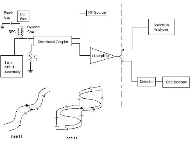
The first point, in understanding rf-SQUID response is to understand its response to a pumped rf signal. For this purpose a test set-up similar to the one in Figure 1.9, having only the rf-components can be assembled. The setup schematic is shown in Figure 2.1
Figure 2.1: A set-up to understand the response of rf-SQUID to an applied rf-pump
In this setup, rf-source supplies the rf power to rf-SQUID tank-circuit assembly via a directional coupler having good isolation (preferably 15 dB larger than the return loss of the tank circuit assembly). The response signal coming from rf-SQUID is taken from the tank circuit assembly through the same coupler and amplified to a detectable level. For detection, a spectrum analyzer or a detector with an oscilloscope can be used. This experiment was also performed where the spectrum analyzer was used. As shown in the figure, there is also a DC-Bias applied to SQUID to change the flux [10], [12]. Two inserts are added in Figure 2.1. These inserts are about the behavior of rf-SQUID (whether hysteretic or not), the information about which are given in 1.3.2 [12].
CHAPTER 2. DESIGN AND IMPLEMENTATION OF AN EXPERIMENTAL RF-SQUID READ-OUT SYSTEM
Firstly, via DC bias, the working point of rf-SQUID is selected (thick dots on the inserts of Figure 2.1) for both hysteretic case and non-hysteretic case. An applied rf signal into the tank circuit will create rf flux on the SQUID and as indicated by arrows in the inserts of Figure 2.1, the SQUID working point moves. If the rf power is further increased, the extent of this movement gets wider.
For the hysteretic operation of rf-SQUID, if the rf power is increased, an excursion around one hysteresis loop takes place. The excursion is dissipative, thus the rf energy is absorbed by the SQUID at the hysteresis loops. After hysteresis loops, the envelope increases again. This increase (build-up) is slow depending on the Q of the tank circuit. As soon as the rf voltage reaches its former value, a new excursion around a hysteresis loop takes place. In Figure 2.2, the upper trace shows this case. When the applied rf-power is increased, the build up speed on the tank circuit increases as seen in the lower trace of Figure 2.2. When the rf power reaches a value at which the build up takes place only in one cycle, the SQUID goes into a second hysteresis loop and upper trace is seen again [12], [13].
CHAPTER 2. DESIGN AND IMPLEMENTATION OF AN EXPERIMENTAL RF-SQUID READ-OUT SYSTEM
In a hysteresis loop, the energy dissipated in the SQUID is [13],
2
0 c c
E I LI
∆ = Φ = (2.1)
where L is the effective inductance of the SQUID and Ic is the critical current of the
junction.
According to these results, the relation between the applied rf signal and the voltage response of rf-SQUID will look like a staircase pattern similar to the plot in Figure 2.3. At the plateau of steps, a hysteresis loop is traversed and on other parts, no modulation is added to the rf pump signal. Also according to the same figure, when the initial dc bias is changed, the staircase shifts (in Figure 2.3, two extreme cases of initial biases are shown) [12], [13].
Figure 2.3: Staircase pattern for different DC biases
CHAPTER 2. DESIGN AND IMPLEMENTATION OF AN EXPERIMENTAL RF-SQUID READ-OUT SYSTEM
For the non-hysteretic case, a rigorous theoretical analysis results in the similar stair case pattern [27].
In another mode of operation, without any dc-bias, a low rf power (-60dBm to – 90dBm) is applied to the SQUID, such that, during its cycle, no quantum transition takes place. For this purpose the critical rf magnetic flux cannot exceed
0 1 4 rf L Is Φ Φ = + (2.2)
In equation 2.2, L is the effective inductance of the rf-SQUID and Is 1 is the supercurrent
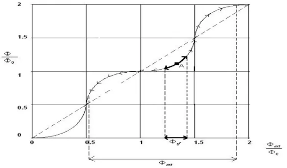
in the loop. At this point an externally applied low frequency signal creates magnetic flux via a coupling coil on the tank circuit and the bias position of the rf-signal sweeps. This case is best understood from Φextvs. Φ curve indicated in Figure 1.7. Similar
figure with the effects of rf power and externally applied flux is shown in Figure 2.4. The extent of Φextis much larger than Φrf and when applied together, Φrf sweeps over
ext
Φ on the flux curve. According to Figure 2.3, an appliedΦextcauses Φrf to sweep
between the two staircase patterns [12], [13]. Thus an amplitude modulation is applied to the rf power whose envelope has a triangular-like relation with the applied external flux as indicated in Figure 2.5. On this figure, B1 and B2 refer to the biasing conditions indicated in Figure 2.3 [12].
CHAPTER 2. DESIGN AND IMPLEMENTATION OF AN EXPERIMENTAL RF-SQUID READ-OUT SYSTEM
Figure 2.4: The effect of externally applied low frequency signal flux together with rf power flux
Figure 2.5: Envelope of the response of rf-SQUID vs. applied flux in second mode of operation for different initial biasing conditions, B1 and B2.
CHAPTER 2. DESIGN AND IMPLEMENTATION OF AN EXPERIMENTAL RF-SQUID READ-OUT SYSTEM
This last mode of operation is widely used, which is the mode of operation exploited in this work. A typical plot of implemented system is shown in Figure 2.6. The operation principle of this system is very similar to that indicated in Figure 2.1 but with some differences.
• In place of DC bias, a signal generator is used.
• Instead of a detector, a mixer is used (which is in fact a detector, but requiring in-phase rf-signal to acquire base-band envelope)
Figure 2.6: A typical plot of implemented system
CHAPTER 2. DESIGN AND IMPLEMENTATION OF AN EXPERIMENTAL RF-SQUID READ-OUT SYSTEM
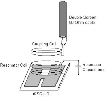
2.2 Tank Circuit Assembly
RF-SQUID tank circuit is one of the main parts of a SQUID system, where the coupling is achieved through. It plays the role of an antenna in a microwave transmitter/receiver assembly.
The tank circuit is mainly a resonator resonating at a specified frequency. At this frequency, it pumps the flux created by RF wave coming from the transmitter subsystem into the SQUID biasing it. At the biasing condition, the output voltage of the rf-SQUID is the periodic function of the flux [29].
In the literature on the rf-SQUID research, different types of resonators have been proposed. These resonators include planar and lumped element tank circuits. Planar resonators are produced on the fundamentals of coplanar waveguide technology and made of superconducting thin-films. One of the advantages of these resonators is their high quality factor (Q) whose effect will be shown. Information about coplanar resonators and their coupling to rf-SQUID can be found at [31].
For lower frequencies, several research groups have proposed different topologies for tank circuits [13]. In this work, the utilized tank circuit has a different topology as shown in Figure 2.7 [32].
CHAPTER 2. DESIGN AND IMPLEMENTATION OF AN EXPERIMENTAL RF-SQUID READ-OUT SYSTEM
Figure 2.7: Utilized tank circuit topology
As stated before, there are two modes of operation of the rf-SQUID, hysteretic and non-hysteretic. In this section, the relation between the SQUID parameters and the tank circuit parameters are investigated for the non-hysteretic case. The same analysis for the hysteretic case is out of the scope of this work.
When an rf signal together with the low frequency signal are applied to the tank circuit, the low frequency signal is coupled to the SQUID via the coupling coil, and the rf power is coupled through the tank circuit resonating at a certain frequency. But the created flux by the signals applied to the tank circuit assembly affects the effective inductance of the rf-SQUID, Leff , where,
CHAPTER 2. DESIGN AND IMPLEMENTATION OF AN EXPERIMENTAL RF-SQUID READ-OUT SYSTEM
1 1 cos eff s l L L β φ = + (2.3)
In this equation, β is the hysteresis parameter, and l φis the phase shift caused by the
applied flux (
0
2
φ = π Φ
Φ ) (Section 1.3.2). Since there is a transformer relation between
the SQUID inductance and the tank circuit inductance, there would be a coupling between them, k, and the mutual inductance, M [29]. Then the equivalent inductance of the tank circuit becomes
2 1 s T eff k L L L L = − (2.4)
in which L is the inductance of the coil. The relation between the coupling and the mutual inductance is 2 2 s eff M k L L
= [34]. Having found the equivalent tank inductance, the tank circuit resonation frequency becomes
0 2 1 cos( ) 1 1 cos( ) T l l w w L C k β φ β φ = = − + (2.5) where 0 1 w LC = (2.6)
and C is the tank circuit capacitance [29]. If the Josephson junction used in the SQUID is not a 0-junction, an extra phase shift is required, ξ, and equation 2.5 becomes
CHAPTER 2. DESIGN AND IMPLEMENTATION OF AN EXPERIMENTAL RF-SQUID READ-OUT SYSTEM
0 2 1 cos( ) 1 1 cos( ) T l l w w L C k β φ ξ β φ ξ = = − + + + (2.7)
for the SQUID operation, the maximum extent of the frequency shift must be larger than the bandwidth of the tank circuit, which is
0 T w w Q ∆ = (2.8)
then the maximum extent of the operating frequency of rf-SQUID from equation 2.7 is;
2 2 2 0 (1 )(1 ) l l k w w k β β ∆ ≈ − − (2.9)
We need ∆ > ∆w wT for proper operation of the tank circuit and this condition is provided by; 2 2 2 1 (1 )(1 ) l l k Q k β β > − − (2.10)
According to this equation, higher Q and higher coupling coefficient between tank circuit inductance and the effective inductance of the SQUID is required for rf-SQUID operation bandwidth to cover tank circuit bandwidth [29], [13].
Some of the important parameters of the tank circuit are as follow:
CHAPTER 2. DESIGN AND IMPLEMENTATION OF AN EXPERIMENTAL RF-SQUID READ-OUT SYSTEM
• As pointed out in equation 2.10, coupling mechanism is important, since it quantifies the magnetic flux linkage into the SQUID sensor. The inter-winding capacitance, winding method used, geometry of coils, spacing between coils, shielding and focusing of SQUID affect the coupling [34], [35]. Design of an effective transformer is a matter of experience [24].
• Reflection parameter (S11) of a tank circuit determines the amount of power that is sent into tank circuit assembly for a characteristic impedance of Z0. It is
also named as return loss, and formulated as the ratio of the reflected power (Pin-) to the incident power (Pin+).
10 10log ( in ) in P RL P − + = − (2.11)
For a tank circuit to function properly, it should have a low RL to transfer all the power at its terminals into rf-SQUID [36]. The S11 of a tank circuit is shown in Figure 2.8.
Figure 2.8: A typical plot of tank circuit S11
CHAPTER 2. DESIGN AND IMPLEMENTATION OF AN EXPERIMENTAL RF-SQUID READ-OUT SYSTEM
• Bandwidth or Q is another parameter, whose effect was demonstrated in equation 2.10. It defines the frequency extent of a circuit’s response, at which the amplitude response at one extent is 3dB below its pass-band amplitude response. This is important in noise analysis, since it affects the selectivity (indirectly noise bandwidth) of the tank circuit [13].
• Electromagnetic shielding is also important for the tank circuit. Environmental in-band signals are amplified together with the main SQUID signal. They cause interferences in the receiver. In some cases, they might lead to oscillations, stealing rf-power from the main SQUID signal [24].
2.3 RF Subsystems Design
Section 2.1 describes the major points in rf-SQUID functioning and the modulation created by the rf-SQUID on the applied rf-power. For a proper detection, the rf-power must be sent in a controlled manner and the received power should be clearly transported to mixer. After mixer, the required amplification and filtering should be made to read rf-SQUID response in a clear manner.
In this work, the system in Figure 2.6 is established. The implemented system has mainly 2 parts, which are the transmitter and the receiver (including IF). The system is homodyne type, in which direct down-conversion to base-band is achieved via the same carrier signal.
CHAPTER 2. DESIGN AND IMPLEMENTATION OF AN EXPERIMENTAL RF-SQUID READ-OUT SYSTEM
2.3.1 Transmitter (Tx)
Transmitter is one of the important blocks in the system of Figure 2.6. Its main function is to send power into both SQUID and the mixer. A local oscillator (LO) provides rf-signal and then it is divided to feed both rf-SQUID and the mixer. A block diagram of this part is shown in Figure 2.9.
Figure 2.9: Transmitter Subsystem
The first important point to notice is the LO output. It is selected to be +8dBm (the used LO has this level of output power). Also, an attenuator is used as a buffer for the mismatches at the output of the LO, [35].
CHAPTER 2. DESIGN AND IMPLEMENTATION OF AN EXPERIMENTAL RF-SQUID READ-OUT SYSTEM
After the LO, there is a power divider with two channels. The channel on the left of Figure 2.9 sends rf-signal into rf-SQUID. This channel attenuates the rf-signal to lower values (-60dBm to –90dBm). For adjustment, a digital attenuator is added on the channel, and it has an attenuation range of –32dB to –64dB. In this manner the transmitted power can be adjusted to well defined values [12], [13].
In fact, this part of the circuit does not look like a conventional transmitter, at which the power is amplified. Also, since we do send only the carrier (no added modulation), there are no strict linearity constraints of the stages.
The channel on the right side of Figure 2.9 is the second part of the transmitter stage. Its function is to amplify the LO signal to a level required by the mixer (+17dBm). An amplifier and a filter are used on the strip together with the attenuators (for buffering). Here the filter is used to prevent the out of band signals going into mixer. The source of these signals might be the amplifier (2nd order IP products or 3rd order IM) [24] or environmental signals amplified by the amplifier (in inadequate shielding).
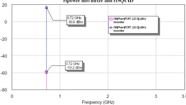
Figure 2.10 shows a simulation of the transmitter subsystem. On the figure, the power at the output of the two channels for a frequency of 720 Mhz is shown. For 64 dB of attenuation in the digital attenuator, the power going into rf-SQUID is –93 dBm.
CHAPTER 2. DESIGN AND IMPLEMENTATION OF AN EXPERIMENTAL RF-SQUID READ-OUT SYSTEM
Figure 2.10: Rf power spectrum for 720 MHz frequency at the output of two channels of the transmitter subsystem
2.3.2 Receiver (Rx)
The most important block of the system is the receiver. This is a critical block since the received signal should be transported to the mixer and the IF stages with lowest possible distortion. It is shown in 2.1 that, SQUID’s response is an AM modulated signal [13] and AM modulation requires linear processing [24], [37], [38]. In section 1.4, some properties of a typical receiver system are called and these properties are analyzed in this subsection.
Receiver’s schematic circuit is shown in Figure 2.11. According to the figure, the power from the transmitter is sent into rf-SQUID assembly via the coupler. Also a bias-CHAPTER 2. DESIGN AND IMPLEMENTATION OF AN EXPERIMENTAL
tee is added between tank circuit assembly and the coupler to couple the low frequency flux into the rf-SQUID. The modulated rf-signal coming from the tank circuit assembly is sent into the receiver strip via the coupler and the signal is amplified. After this amplification, the signal is taken into the mixer together with the high power coming from the transmitter to get the base-band signal. Lastly, the base-band signal (the envelope on the rf signal) is filtered and amplified.
Figure 2.11: Receiver, Schematic View
Although detailed specification data sheets are added, some important characteristics of the utilized devices are shown in Table 2.1 - Table 2.4.
CHAPTER 2. DESIGN AND IMPLEMENTATION OF AN EXPERIMENTAL RF-SQUID READ-OUT SYSTEM
Amplifier
Name SCA-4
Frequency Range 0.1-3GHz
Power Gain 18dB
Output 1dB Compression Point 19dBm
Noise Figure 4.5dB
IP3 38dBm
Isolation 22dB
VD 5V
Table 2.1:Amplifier Properties
Filter
Bandwidth 0.6-0.9GHz
Loss 2 dB
Rejection 50 dB at 0.4GHz
50 dB at 1.1 GHz
Power Rating (experienced) 20dBm Table 2.2: Filter Characteristics
Mixer Name ZFM-2H Frequency Range RF 5MHz-1GHz LO 5MHz-1GHz IF DC-1GHz Conversion Loss 7dB
CHAPTER 2. DESIGN AND IMPLEMENTATION OF AN EXPERIMENTAL RF-SQUID READ-OUT SYSTEM
LO Power 17dBm
RF-LO Isolation 35dB
LO-IF Isolation 25dB
Input 1dB compression 14dBm
Input IP3 21 dBm
Table 2.3: Mixer properties
Also utilized coupler is a 3 dB coupler, the isolation of which is over 30 dB in the band of interest (600MHz-900MHz). Bias-Tee’s loss can be neglected (very low) and the attenuators between each stage are used for increasing match between each device. The filter and the amplifier after the mixer are assembled in an instrument by SRS1.
The important receiver parameters stated in section 1.4, and their effects are as follows:
• Receiver Sensitivity
Receiver sensitivity is a fundamental property for system performance. In this part, device gains and noise figures are treated separately to find total noise factor. In view of this analysis, receiver sensitivity is found [24].
The noise factor in a receiver is [24]
3 2 1 1 1 1 1 2 0 1 1 1 ... 1 n i IN i i j j F F F F F G G G G − = = − − − = + + + = +
∑
∏
(2.12) iF : Noise factor of ith stage (linear)
CHAPTER 2. DESIGN AND IMPLEMENTATION OF AN EXPERIMENTAL RF-SQUID READ-OUT SYSTEM
i
G : Gain of ith state (linear)
After the calculation of the effective noise factor of the receiver, sensitivity of the receiver can be calculated from;
0
( 1)
IN
e= F kTB R− Z (2.13)
where the parameters are defined as:
E: receiver sensitivity (V) k: Boltzmann’s constant (J/K)
T: temperature (K)
B: Equivalent Noise Bandwidth (Hz) R: 1+SNR at the input (linear) Z0: System impedance
For the analysis, following assumptions are made: The power coming from rf-SQUID is around –70 dBm, the bandwidth of the system is 30 kHz (determined by the IF circuit), and all the stages are matched to each other. The results of the analysis are shown in Table 2.4 through Table 2.6.
CHAPTER 2. DESIGN AND IMPLEMENTATION OF AN EXPERIMENTAL RF-SQUID READ-OUT SYSTEM
Stage # 1 2 3 4 5 6 7 8 9 10 11 12 Stage Dir. Coup. Amp. Atten. Amp. Att. Filter Att. Amp. Att Mixer filter Amp.
Gain(dB) -3.2 18 -2 18 -2 -2.5 -2 18 -2 -7 -1 50 NF(dB) 3.2 4.5 2 4.5 2 4.5 2 4.5 1 7 1 NA Output IP3(dBm) 100 38 100 38 100 100 100 38 100 20 100 40 Output Power (dBm) -73.2 -55.2 -57.2 -39.2 -41.2 -43.7 -45.7 -27.7 -29.7 -36.7 -37.7 12.3 Input Power (dBm) -70 -73.2 -55.2 -57.2 -39.2 -41.2 -43.7 -45.7 -27.7 -29.7 -36.7 -37.7 Total Gain (dB) -3.2 14.8 12.8 30.8 28.8 26.3 24.3 42.3 40.3 33.3 32.3 82.3
Table 2.4: Noise and Power in each stage of the receiver system
Input Power -70 dBm Analysis temperature 25 o C Noise Bandwidth 30 KHz Required S/N 10dB Noise Source 290K
CHAPTER 2. DESIGN AND IMPLEMENTATION OF AN EXPERIMENTAL RF-SQUID READ-OUT SYSTEM
Gain 32.3 dB for rf, adjustable IF NF 7.79dB Noise Temp 1454.3K SNR 51.41dB Sensitivity -111dBm Noise Floor -166dBm/Hz Input IP3 -42dBm Output IP3 40dBm
Table 2.6: Results characterizing the receiver
According to the results, the receiver is able to respond signals at –111dBm level (on 50 Ohm, Z0) with an SNR of 10dB.
• Selectivity
Receiver selectivity is another important parameter of the characteristics of the receiver. It quantifies the tendency of a receiver to respond to channels adjacent to the desired reception channel [24]. In this work, only one channel is utilized for rf-SQUID operation and there is no adjacent channel-filtering requirement. Thus, the IF filter’s bandwidth was tuned to filter only the received modulation. In the future, for multi-channel rf-SQUID based systems and operation, the receiver selectivity will become important. Hence the related equations are also included in this report [24]. For selectivity we have;
( /10) ( /10) ( /10)
10log[10 IFsel 10 Spurs 10SBN ]
Selectivity= −CR− − + − +BWx (2.14)
where in equation 2.14 [24]
CHAPTER 2. DESIGN AND IMPLEMENTATION OF AN EXPERIMENTAL RF-SQUID READ-OUT SYSTEM
Selectivity : Amount of adjacent channel selectivity (dB)
CR : Co-channel rejection (dB)
sel
IF : IF filter rejection at the adjacent channel (dB)
Spurs : LO spurious signals in the if bandwidth at a frequency offset of channel spacing (dBc)
BW : IF noise bandwidth (dBc)
SBN : SSB phase noise of LO at channel spacing (dBc/Hz)
• Receiver Spurious Responses
These signals are unwanted signals but they again produce signals in the IF bandwidth. The mixer according to equation 2.15 mostly produces them [39], [40] as;
rf LO IF
mf nf f
± ± = ± (2.15)
where m and n are the integer multipliers of RF frequency and LO frequency. The created spurious frequencies are
1 2 LO IF rf LO IF rf nf f f m nf f f m − = + = (2.16)
Following these equations, the (m,n) indices that can be mapped near our IF frequency are as follows [24], [39], [40]:
CHAPTER 2. DESIGN AND IMPLEMENTATION OF AN EXPERIMENTAL RF-SQUID READ-OUT SYSTEM
v (-1,1) for low-side injection (fLO<fRF) and (1, -1) for high side injection
(fLO>fRF). The effect of these products was analyzed in sensitivity
analysis. They cause noise to be increased.
v (2, -2) for low-side injection and (-2,2) for high side injection. It causes 2fIF to be appeared at the output of the mixer. For 20 KHz of IF
frequency, 40 KHz signal can be viewed at the output which is limited by the IF filter used and the 2nd order intercept point (IP2) performance of the mixer.
v Higher order spurious signals resulting from higher order combinations of m and n. These are also limited by the IF filter directly following IF port of the mixer and the mixer performance for higher order products. Higher IF frequencies should be selected but in rf-SQUID operation, we are limited by the responses of rf-SQUID.
v If the LO is synthesized, spurious signals in its spectrum due to reference frequency and its harmonics may result. These signals can cause mixer to create close IF signals.
• 3rd Order Intercept Point (IP3)
IP3 is a measure of system linearity. It is a theoretical point at which the desired signal and the third order distortion products are equal in amplitude. In Figure 2.12, a graphical description of intercept point and 3rd order intercept is shown [24], [36], [40], [41].
CHAPTER 2. DESIGN AND IMPLEMENTATION OF AN EXPERIMENTAL RF-SQUID READ-OUT SYSTEM
Figure 2.12: Intercept Point Definition and IP3
IP3 was found in the sensitivity analysis, for which equation 2.17 was used. In this equation all values are in terms of mW.
1 1 1 INPUT N j j IP IP = =
∑
(2.17)In our system, input IP3 is found as –32.3 dBm and the maximum signal returning from rf-SQUID is around –70 dBm (far from non-linearity).
CHAPTER 2. DESIGN AND IMPLEMENTATION OF AN EXPERIMENTAL RF-SQUID READ-OUT SYSTEM
2.3.3 Flux Feeding
Flux feeding is a key part of the operation of the system. According to Figure 2.11, an ac flux is given via a bias tee. The main aim of the ac flux is to change the biasing of rf-SQUID continuously as indicated in Figure 2.4 [13].
In Figure 2.7, there are two coils, one of which is the coupling coil. This coil together with the tank circuit coil helps resonance at the required frequency. Besides, it is this coil through which ac flux is fed to the rf-SQUID.
2.4 Implementation of rf-SQUID Read-Out System
Up to this point, system design of read-out electronics were investigated. The implementation of the system is made in blocks as indicated in Figure 2.6. Also the theoretical details about these subsystems are shown in Figure 2.9 and Figure 2.11. The specification sheets about the circuit elements are included in Appendix.
Before implementation, the measurements related to circuit elements (schematic view) and the subsystems are covered in this section. These measurements include
• S-parameters
• 1dB compression point, IP2 and IP3 (for the amplifiers)
• Coupling and isolation parameters (for the power dividers and couplers) CHAPTER 2. DESIGN AND IMPLEMENTATION OF AN EXPERIMENTAL RF-SQUID READ-OUT SYSTEM
2.4.1 Measurements Related to Devices and Subsystems
• Amplifier
In the Appendix, the specifications of the used amplifier (SCA-4, MA-COM) are given. Some measurements are performed to verify these specifications. These measurements include S-parameters, 1dB compression point, 2nd order intercept point, and 3rd order intercept point.
Firstly S-parameters are measured. A network analyzer (Model Number : 8753D) is used for the measurement of the S-parameters of the amplifier.
S11 and S21 -20.0 -15.0 -10.0 -5.0 0.0 5.0 10.0 15.0 20.0 25.0 600 700 800 900 1000 Frequency(MHz) S21 and S11 (dB) S11(dB) S21(dB)
Figure 2.13: Amplifier S11 and S21
CHAPTER 2. DESIGN AND IMPLEMENTATION OF AN EXPERIMENTAL RF-SQUID READ-OUT SYSTEM
S22 and S12 -25.0 -20.0 -15.0 -10.0 -5.0 0.0 600 700 800 900 Frequency (MHz) S22 and S12 S12(dB) S22 (dB)
Figure 2.14: Amplifier S22 and S12
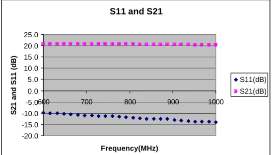
In Figure 2.13 and Figure 2.14, the measured S-parameters of amplifier are shown. S11 lower than –10 dB is compatible for the application. Together with the use of the attenuators between each device in the receiver (Figure 2.11), S11 and S22 can be improved. S21 is over 20 dB and S12, in other words the isolation of the amplifier, is around 23 dB.
Other parameters of interest are the 1dB compression point, IP2, and IP3. Figure 2.15 through Figure 2.18 show the measurements related to these parameters.
CHAPTER 2. DESIGN AND IMPLEMENTATION OF AN EXPERIMENTAL RF-SQUID READ-OUT SYSTEM
1dB Compression -20 -15 -10 -5 0 5 10 -20 -15 -10 -5 0 5 Input Power Output Power Input Power vs Output Ideal Input vs Output
Figure 2.15: 1dB compression point of the amplifier
Gain Decrease vs Input Power
-0.5 0 0.5 1 1.5 2 2.5 3 3.5 4 -20 -15 -10 -5 0 5 Input Power Gain Decrease Gain Decrease vs Input Power
Figure 2.16: Gain decrease for the exact measurement of 1dB compression CHAPTER 2. DESIGN AND IMPLEMENTATION OF AN EXPERIMENTAL RF-SQUID READ-OUT SYSTEM
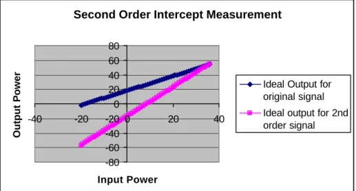
Second Order Intercept Measurement -80 -60 -40 -20 0 20 40 60 80 -40 -20 0 20 40 Input Power Output Power
Ideal Output for original signal Ideal output for 2nd order signal
Figure 2.17: IP2 measurement
3rd order intercept measurement
-80 -60 -40 -20 0 20 40 60 -20 -10 0 10 20 Input Power(dBm) Output Power(dBm) Ideal Output Ideal output for 3rd order signal
Figure 2.18: IP3 measurement
P1dB -1 dBm at the input
IP2 35 dBm at the input
IP3 16dBm at the input
Table 2.7: Power measurements of amplifier
CHAPTER 2. DESIGN AND IMPLEMENTATION OF AN EXPERIMENTAL RF-SQUID READ-OUT SYSTEM
Also noise figure measurement of the amplifier was performed with a calibrated noise source and a 4.21 dB was measured.
• Attenuator
Attenuators are used between each device and the SQUID output of the transmitter. They are used to increase the match between the devices and regulate the power going into the rf-SQUID (A digital attenuator is used for this purpose having similar properties as other attenuators). A typical S parameter measurement of a 3dB attenuator is shown in Figure 2.19. S11 and S21 of a 3dB attenuator -2.50E+01 -2.00E+01 -1.50E+01 -1.00E+01 -5.00E+00 0.00E+00 600 650 700 750 800 850 900 Frequency (MHz) S11 and S21 (dB) S11 S21
Figure 2.19: S parameter measurement of an attenuator
• 3dB Coupler
In section 2.1 and 2.3, the role of the coupler in sending and receiving power from the CHAPTER 2. DESIGN AND IMPLEMENTATION OF AN EXPERIMENTAL
degrees coupler for which the through port and coupled port are 180 degrees out of phase. This property of coupler is not utilized in this work. The S parameters related to the coupler (coupled port S21, through S21, S11 (at the transmitter side) and isolation) are reported below.
S11 and S21 of coupler -2.50E+01 -2.00E+01 -1.50E+01 -1.00E+01 -5.00E+00 0.00E+00 600 650 700 750 800 850 900 Frequency(MHz) S11 and S21(dB) S11(dB) S21(dB)
Figure 2.20: S11 and S21 of the coupler
In Figure 2.20, S21 parameter is found for the through port, where it is also similar for the coupling port except for the phase, which is 180 degrees out of phase.
Isolation (dB) -3.44E+01 -3.42E+01 -3.40E+01 -3.38E+01 -3.36E+01 -3.34E+01 -3.32E+01 600 650 700 750 800 850 900 Frequency(MHz) Isolation(dB) Isolation
Figure 2.21: Isolation parameter of the coupler
CHAPTER 2. DESIGN AND IMPLEMENTATION OF AN EXPERIMENTAL RF-SQUID READ-OUT SYSTEM
According to Figure 2.6, the transmitter and the receiver sub-blocks are connected to the isolated ports of the coupler. So power coming from the transmitter is isolated from the receiver by the isolation parameter shown in Figure 2.21.
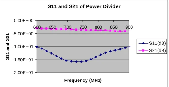
• Power Divider
Power Divider is used in some parts of the transmitter and the receiver. In Figure 2.9, transmitter has two arms and these two arms are connected to the mixer and the coupler. To achieve this, division in microwave frequencies is done with power dividers. A power divider with moderate isolation was designed for this work [39]. The measured S-parameters of it are as follows;
S11 and S21 of Power Divider
-2.00E+01 -1.50E+01 -1.00E+01 -5.00E+00 0.00E+00 600 650 700 750 800 850 900 Frequency (MHz) S11 and S21 S11(dB) S21(dB)
Figure 2.22: S11 and S21 related to designed power divider CHAPTER 2. DESIGN AND IMPLEMENTATION OF AN EXPERIMENTAL RF-SQUID READ-OUT SYSTEM
Isolation (dB) -3.00E+01 -2.50E+01 -2.00E+01 -1.50E+01 -1.00E+01 -5.00E+00 0.00E+00 600 700 800 900 Frequency(MHz) Isolation Isolation (dB)
Figure 2.23: Isolation parameter of power divider
Figure 2.22 shows the S-parameters of only one arm. The second arm is symmetric to this arm and similar S-parameters result. Isolation is better than 15 dB as shown in Figure 2.23.
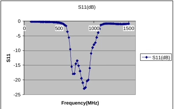
• Filter
Filter is a critical component in almost all rf-systems. It is used in three places in this work. In the receiver it decides the operating bandwidth, in transmitter it filters harmonics of LO signal that feeds the LO port of the mixer, and at the output of the LO for filtering out of band harmonics that can cause wrong measurements. The filter should be selective and have S11 < -10dB.
CHAPTER 2. DESIGN AND IMPLEMENTATION OF AN EXPERIMENTAL RF-SQUID READ-OUT SYSTEM
S11(dB) -25 -20 -15 -10 -5 0 0 500 1000 1500 Frequency(MHz) S11 S11(dB)
Figure 2.24: S11 parameter of filter
S21(dB) -1.20E+02 -1.00E+02 -8.00E+01 -6.00E+01 -4.00E+01 -2.00E+01 0.00E+00 0 500 1000 1500 2000 2500 3000 Frequency(MHz) S21 S21(dB)
Figure 2.25: S21 of the filter
CHAPTER 2. DESIGN AND IMPLEMENTATION OF AN EXPERIMENTAL RF-SQUID READ-OUT SYSTEM
Figure 2.24 and Figure 2.25 show the S parameters of the filter. It should be pointed out that in S21, for higher frequencies, there are jumps, which are due to the box resonance. Different patterns with conducting materials should be implemented in the box to decrease the level of the resonance [24], [40].
• Cables
As pointed out earlier, the implemented system is an experimental system and during the work, modifications can be made for optimum performance. For this purpose, different devices were soldered on PCBs and boxed with copper foils. On each board, SMA connectors are soldered. The connection between each box is made by 50-Ohm rf cables. Thus, rf cables also become a part of the system, whose S parameters are shown in Figure 2.26. The measured cable is 10 inches long.
Cable S parameters -3.50E+01 -3.00E+01 -2.50E+01 -2.00E+01 -1.50E+01 -1.00E+01 -5.00E+00 0.00E+00 5.00E+00 600 650 700 750 800 850 900 Frequency (MHz) S11 and S21 S11(dB) S21(dB)
Figure 2.26: 10 inch cable S-parameters
CHAPTER 2. DESIGN AND IMPLEMENTATION OF AN EXPERIMENTAL RF-SQUID READ-OUT SYSTEM
In this figure, it is clear that these cables are not strictly 50 Ohm, but have good enough characteristics for this application.
• Mixer
The mixer of the system is tested for the conversion loss associated with it. For this test, HP 8656B and HP 8657B signal generators are used on a same time basis. HP 8590L spectrum analyzer is used to view the spectrum at the IF port of the mixer. The experiment setup is shown in Figure 2.27.
Figure 2.27: Established Setup to measure mixer
CHAPTER 2. DESIGN AND IMPLEMENTATION OF AN EXPERIMENTAL RF-SQUID READ-OUT SYSTEM