Research Article
Temperature Dependent Electrical Transport in
Al/Poly(4-vinyl phenol)/
p-GaAs Metal-Oxide-Semiconductor by
Sol-Gel Spin Coating Method
Fadan Özden,
1Cem Tozlu,
2and Osman Pakma
31Department of Physics, Faculty of Sciences, Mu˘gla Sıtkı Koc¸man University, 48170 Mu˘gla, Turkey
2Department of Energy Engineering, Faculty of Engineering, Karamano˘glu Mehmetbey University, 70100 Karaman, Turkey 3Department of Physics, Faculty of Arts and Sciences, Batman University, 72000 Batman, Turkey
Correspondence should be addressed to S¸adan ¨Ozden; [email protected] Received 6 January 2016; Accepted 24 February 2016
Academic Editor: Mahmoud M. El-Nahass
Copyright © 2016 S¸adan ¨Ozden et al. This is an open access article distributed under the Creative Commons Attribution License, which permits unrestricted use, distribution, and reproduction in any medium, provided the original work is properly cited. Deposition of poly(4-vinyl phenol) insulator layer is carried out by applying the spin coating technique onto p-type GaAs substrate so as to create Al/poly(4-vinyl phenol)/p-GaAs metal-oxide-semiconductor (MOS) structure. Temperature was set to 80–320 K while the current-voltage (I-V) characteristics of the structure were examined in the study. Ideality factor (n) and barrier height (𝜙𝑏) values found in the experiment ranged from 3.13 and 0.616 eV (320 K) to 11.56 and 0.147 eV (80 K). Comparing the thermionic field emission theory and thermionic emission theory, the temperature dependent ideality factor behavior displayed that thermionic field emission theory is more valid than the latter. The calculated tunneling energy was 96 meV.
1. Introduction
Compound semiconductor materials can be used in such applications to achieve better results. Currently, many dif-ferent compound semiconductors are available, but, among them, gallium arsenide (GaAs) has been the most studied one since the technologies used to process and fabricate this material have been highly developed [1–4]. Due to its direct energy bandgap, GaAs is ideally preferred for light emission and photovoltaic devices. It also has a wide bandgap (1.5 eV)
and high electron mobility (8000 cm2V−1s−1), which has
specific advantages in operations requiring high frequency and temperature [5].
The interest in and the efforts toward developing new organic-based electronic and optoelectronic devices have recently increased. Charge carrier injection from electrodes into organic material constitutes one important factor to determine the device function and performance for metal-semiconductor (MS) devices [6]. Modification of the electri-cal properties of (MS) Schottky structures can be achieved by using an organic semiconductor. In this technique, an organic
interfacial layer is inserted between inorganic semiconductor and metal. As they can be applied to various areas like solar cells and Schottky diodes, there has been a growing interest in polymers such as poly(4-vinyl phenol), polyani-line, polyvinyl alcohol (PVA), poly(alkylthiophene) polypyr-role, polythiophene, and poly(3-hexylthiophene) [7–18]. In polymers, we find local free-volume holes or cavities of atomic and molecular dimensions, which may be the result of irregular packing of the molecules in amorphous phase (static and preexisting holes) and molecular relaxation of polymer chains and terminal ends (dynamic and transient holes). The density of the amorphous phase declines due to these holes approximately by 10%, when compared to that of the crystalline phase of the same polymeric material. Thus, such free-volume holes found in a polymeric system influence the polymer’s optic, thermal, dielectric, electrical, and relaxing properties. For this reason, poly(4-vinyl phenol) is much more preferred as an insulating layer since it has several advantages such as higher device performance, stability, and reliability over other kinds of insulator layers. Therefore, the use of poly(4-vinyl phenol) as a gate insulator material in
Volume 2016, Article ID 6157905, 5 pages http://dx.doi.org/10.1155/2016/6157905
organic field effect transistors (OFETs) has been common [18, 19]. The high performance and reliability of OFETs mainly stem from the insulator layer between metal and semiconductor, as well as from the interface states between semiconductor and insulator and series resistance. Poly(4-vinyl phenol) has been reported to be the best polymeric gate dielectric in terms of mobility [15]. Device performance is significantly affected by gate dielectric, which is an important component of organic thin film transistors (OTFT) [19]. Yet, certain electrical instabilities are found in an OTFT with poly(4-vinyl phenol) used as the gate dielectric, a case which could be exemplified by bias stress effect or hysteresis, leading to shifting threshold voltage depending on the amount of hydroxyl groups and thus to gate leakage current. The reason behind the occurrence of hysteresis is slow polarization as a result of remnant dipoles and charge injection as well as trapping mechanism [20, 21]. Several experimental studies have been carried out to examine the effect of organic materials used as an insulating layer in device applications [22, 23].
In the present study, the current-applied bias voltage-temperature (I-V-T) measurement in darkness was per-formed to clarify the current transport mechanism(s) and electrical features of Al/poly(4-vinyl phenol)/p-GaAs struc-tures.
2. Design and Fabrication of
Al/Poly(4-vinyl phenol)/p-GaAs Structures
A lot of Al/poly(4-vinyl phenol)/p-GaAs structures werefabricated on the 2-inch diameter float zone <111> p-type
(zinc-doped) GaAs wafer with a thickness of 500𝜇m and
a resistivity of 2Ω cm. For the fabrication process, GaAs
wafer was degreased through the RCA cleaning procedure. The RCA cleaning procedure has three major steps that are used sequentially: (I) organic cleaning: removal of insoluble
organic contaminants with a 10-minute boiling in NH4OH +
H2O2 + 6H2O solution, (II) oxide stripping: removal of a
thin oxide layer where metallic contaminants might have
accumulated as a result of (I), using a diluted (30 s) HF : H2O
(1 : 10) solution, and (III) ionic cleaning: the procedure
was followed by a 10-minute boiling in HCl + H2O2 +
6H2O solution [24, 25]. Next, drying was performed in
N2 atmosphere for a prolonged time. Following the drying
process, In-Ag (25%, 75%) with a thickness of 2000> was
thermally evaporated from the tungsten filament onto the whole back surface of the GaAs wafer under the pressure
of 10−6Torr. In order to obtain a low-resistivity ohmic back
contact, GaAs wafer was sintered at 580∘C for 3 min in
N2atmosphere. The poly(4-vinyl phenol) was purchased from
Sigma-Aldrich (Sigma-Aldrich Cat. number 436216) with a molecular weight of 20.000. Spin coating process was applied to cover poly(4-vinyl phenol) on the front surface of the GaAs wafer from 2.5% solution in 2-propanol at 4.000 rpm for 45 s.
The obtained film was cross-linked at 100∘C under vacuum.
In order to obtain a rectifying contact on the front surface of
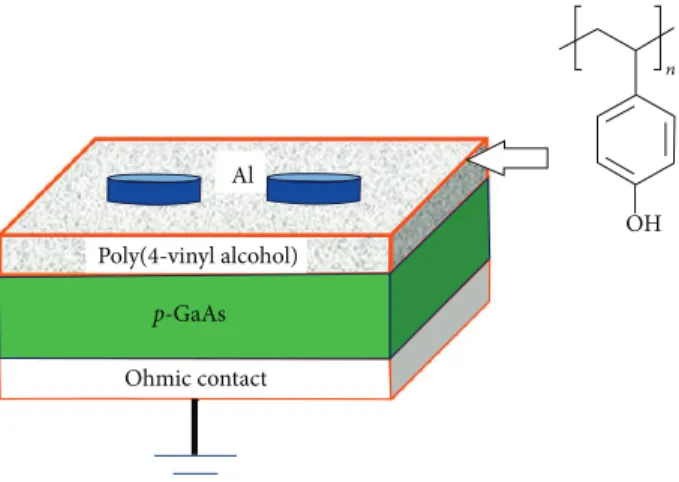
p-GaAs coated with poly(4-vinyl phenol) (Figure 1), a
high-purity aluminum layer was coated on the surface in a high
Al p-GaAs Ohmic contact Poly(4-vinyl alcohol) OH n
Figure 1: Schematic diagram of the Al/poly(4-vinyl phenol)/p-GaAs structure.
vacuum under the pressure of 10−7Torr. The interfacial oxide
layer thickness was estimated to be about 37 nm by Avantes spectrometer (AvaSpec-ULS2048).
The current-voltage (I-V) characteristics of the samples were measured in the temperature range of 80–320 K using
a temperature controlled ARS CS202∗I-DMX-1SS high
per-formance closed cycle cryostat, which allowed us to perform the measurements in the temperature range of 10–325 K, and using a Keithley 4200 programmable constant current source under dark conditions. The sample temperature was contin-ually monitored using a GaAlAs sensor and a Lakeshore 330 autotuning temperature controller with a sensitivity better
than±0.1 K.
3. Measurement and Experimental Results
The current transport across a Schottky junction draws intense interest from both material physicists and device physicist. Usually, a wide range of temperatures are used in determining the Schottky barrier diode (SBD) parameters with the aim of acquiring a better understanding concerning the nature of the barrier and the conduction mechanism. Although, under normal conditions, SBD parameters are obtained through the use of thermionic emission (TE) theory, certain anomalies have been reported at lower temperatures resulting from this theory. The current through a SBD at a forward bias voltage (𝑉 ≥ 3𝑘𝑇/𝑞) based on the TE theory is expressed as [26]𝐼 = 𝐼0[exp ( 𝑞𝑉
𝑛𝑘𝑇) − 1] , (1)
where𝐼0is the reverse saturation current and is described as
𝐼0= 𝐴𝐴∗𝑇2exp(−𝑞𝜙𝑏
𝑘𝑇 ) , (2)
where𝐴, 𝐴∗, 𝑇, 𝑘, 𝑞, and 𝜙𝑏 are the rectifier contact area,
the effective Richardson constant (74 A/cm2K2 for p-type
GaAs), the temperature in Kelvin, the Boltzmann constant, the electron charge, and the barrier height, respectively.
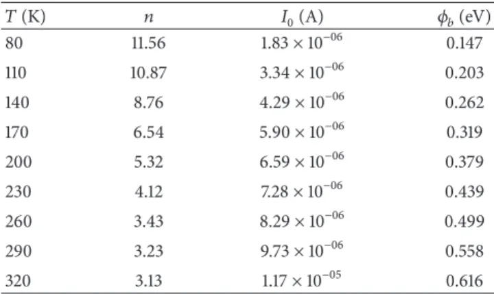
Table 1: The 𝑇, 𝑛, 𝐼0, and 𝜙𝑏 values for the investigated device structure of Figure 1. 𝑇 (K) 𝑛 𝐼0(A) 𝜙𝑏(eV) 80 11.56 1.83× 10−06 0.147 110 10.87 3.34× 10−06 0.203 140 8.76 4.29× 10−06 0.262 170 6.54 5.90× 10−06 0.319 200 5.32 6.59× 10−06 0.379 230 4.12 7.28× 10−06 0.439 260 3.43 8.29× 10−06 0.499 290 3.23 9.73× 10−06 0.558 320 3.13 1.17× 10−05 0.616
The ideality values are derived from the slope of the linear
region of the forward bias ln𝐼-𝑉 plots and can be calculated
from (1) as
𝑛 = 𝑘𝑇𝑞 𝑑𝑉
𝑑 (ln 𝐼). (3)
In Figure 2, a typical temperature dependence is displayed in semilogarithmic plots of I-V characteristics of Al/poly(4-vinyl phenol)/p-GaAs structure under higher voltages. The
I-V plots shift toward the side with higher bias, but a decrease
is observed in temperature. As can be seen in Figure 2, the forward bias I-V characteristics lose a significant amount of their linearity because of the series resistance effect of the Al/poly(4-vinyl phenol)/p-GaAs structure in high voltage
region. The experimental values of𝑛 and 𝜙𝑏by using linear
parts of the I-V characteristics were calculated through
(2) and (3), respectively. Besides,𝑛 and 𝜙𝑏 values of each
temperature are displayed in Table 1. As it is obvious in Figure 3, these two parameters have a strong temperature
dependency. Figure 3 reveals that𝑛 values increased while 𝜙𝑏
values decreased together with a decreasing temperature. The current transport will be dominated by the current flowing through the lower BH and a larger ideality factor due to the temperature activated process [27]. In other words, a higher number of electrons have sufficient energy to overcome the higher barrier when temperature increases and, in turn, BH is increased by temperature and bias voltage.
The conventional Richardson plot of ln(𝐼0/𝑇2) versus
1/𝑘𝑇 was obtained and is shown in Figure 4. The values of activation energy and Richardson constant were obtained
from the slope of this straight line as 0.0178 eV and 2.71×
10−3A/cm2K2, respectively. The Richardson constant value
of 2.71× 10⁻³A/cm2K2is much lower than the known value
of 74 A/cm2K2 for p-type GaAs. As explained above, the
deviation in the Richardson plots might be a result of the spatially inhomogeneous BHs and potential fluctuations at the interface, which consist of low and high barrier areas [28–33]; in other words, the current through the barrier will flow preferentially through the lower barriers in the potential distributions. 0.0 0.2 0.4 0.6 0.8 1.0 1.2 1.4 1.6 1.8 2.0 C u rr en t (A) Voltage (V) Fit region −0.2 10−1 10−2 10−3 10−4 10−5 320 K 80 K ΔT = 20 K
Figure 2: Experimental forward bias ln𝐼-𝑉 characteristics of the Al/poly(4-vinyl phenol)/p-GaAs structure at various temperatures.
50 100 150 200 250 300 0.1 0.2 0.3 0.4 0.5 0.6 0.7 2 4 6 8 10 12 14 T (K) Id ea li ty fac to r, n 𝜙b (eV)
Figure 3: Temperature dependencies of experimental 𝜙𝑏 and 𝑛 values obtained from current versus voltage characteristics of Al/poly(4-vinyl phenol)/p-GaAs structure between 80 and 320 K.
20 40 60 80 100 120 140 160 −11.0 −11.5 −12.0 −12.5 −13.0 −13.5 ln( I0 /T 2) 1/kT (eV−1)
Figure 4: The conventional Richardson plot of ln(𝐼0/𝑇2) versus 1/kT of Al/poly(4-vinyl phenol)/p-GaAs structure.
The high ideality factor value (greater than unity) and its temperature dependence assume that the principally dom-inant factor of the current is the thermionic field emission (TFE). When the TFE theory suggested by Padovani [34, 35] is used to control the current transport, the relationship emerging between the current and voltage can be expressed with the following equation [26]:
𝐼 = 𝐼0exp(𝑞𝑉
𝐸0) (4)
with
𝐸0= 𝐸00coth(𝐸00
𝑘𝑇) = 𝑛tun𝑘𝑇, (5)
where𝐸00is the characteristic tunneling energy that is related
to the tunnel effect transmission probability:
𝐸00= ℎ 4𝜋( 𝑁𝐴 𝑚∗𝜀 𝑠) 1/2 , (6) where𝑁𝐴= 1.3× 1019cm−3,𝑚∗ = 0.6𝑚0 = 0.0402, and 𝜀𝑠 =
12.9𝜀0for p-type GaAs andℎ = 6.626 × 10⁻³⁴Js. The value of
𝐸00/𝑘𝑇 at room temperature was found to be 5.66. However,
the experimental value of𝐸00/𝑘𝑇 at room temperature was
determined as 3.71. If 𝐸00 > 𝑘𝑇, tunneling dominates
since the Boltzmann distribution tail of thermionic emission reduces by a factor of exp{−1} every 𝑘𝑇 and it is much faster when compared to the decrease rate of the tunneling probability [36]. On the other hand, thermionic emission
dominates whenever 𝐸00 ≪ 𝑘𝑇 because the tunneling
probability drops faster than thermionic emission in such a situation. In empirical and practical terms, it is observed that the effect caused by tunneling is small at room temperature
for common semiconductors having a doping level of 1×
1017cm−3or less (𝐸00∼ 3 meV), but it will be pretty significant
for semiconductors with a doping level higher than 1 ×
1018cm−3 (𝐸00∼ 10 meV). In our study, as the doping level
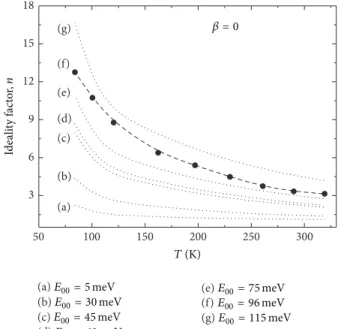
is 1.3× 1019cm−3, tunneling energy is found as 96 meV in our
calculations as can be seen in Figure 5.
4. Conclusions
Measurements of the forward bias I-V characteristics of the Al/poly(4-vinyl phenol)/p-GaAs metal-oxide-semiconduc-tor (MOS) structure were carried out in a temperature range of 80–320 K. Experimental forward bias I-V characteristics were analyzed and an increase was observed in barrier height as well as a decrease in the ideality factor with an increas-ing temperature. Comparincreas-ing the thermionic field emission theory and thermionic emission theory, the temperature dependent ideality factor behavior displays that thermionic field emission theory is more valid than the latter. The calculated tunneling energy was 96 meV.
50 100 150 200 250 300 3 6 9 12 15 18 (a) (b) (c) (d) (e) (f) (g) 𝛽 = 0 T (K) Id ea li ty fac to r, n (a) E00= 5 meV (b) E00= 30 meV (c) E00= 45 meV (d)E00= 60 meV (e) E00= 75 meV (f) E00= 96 meV (g) E00= 115 meV
Figure 5: Thermionic field emission (TFE) fits obtained by fitting (6) to the temperature dependence values of experimental ideality factors calculated for different values of the characteristic energy𝐸00, without considering the bias coefficient of the barrier height,𝛽 = 0, for Al/poly(4-vinyl phenol)/p-GaAs structure. The filled circles show the temperature dependence values of experimental ideality factor obtained from the I-V characteristics.
Competing Interests
The authors declare that there are no competing interests regarding the publication of this paper.
References
[1] C. C. Lee, W. V. Chen, and J. Park, “A new I–V model for light-emitting devices with a quantum well,” Microelectronics Journal, vol. 37, no. 11, pp. 1335–1338, 2006.
[2] S. Kim, D.-M. Geum, M.-S. Park, C. Z. Kim, and W. J. Choi, “GaAs solar cell on Si substrate with good ohmic GaAs/Si interface by direct wafer bonding,” Solar Energy Materials and Solar Cells, vol. 141, pp. 372–376, 2015.
[3] C.-H. Chen, S. M. Baier, D. K. Arch, and M. S. Shur, “A new and simple model for GaAs heterojunction FET characteristics,” IEEE Transactions on Electron Devices, vol. 35, no. 5, pp. 570– 577, 1988.
[4] R.-H. Horng, M.-C. Tseng, and S.-Y. Lien, “Reliability analysis of III-V solar cells grown on recycled GaAs substrates and an electroplated nickel substrate,” International Journal of Photoen-ergy, vol. 2013, Article ID 108696, 9 pages, 2013.
[5] A. Dargys and J. Kundrotas, Handbook on Physical Properties of Ge, Si, GaAs and InP, Science and Encyclopedia, Vilnius, Lithuania, 1994.
[6] N. Koch, A. Kahn, J. Ghijsen et al., “Conjugated organic molecules on metal versus polymer electrodes: demonstration of a key energy level alignment mechanism,” Applied Physics Letters, vol. 82, no. 1, pp. 70–72, 2003.
[7] A. A. M. Farag, E. A. A. El-Shazly, M. Abdel Rafea, and A. Ibrahim, “Optical, electrical and photovoltaic characteristics of
organic semiconductor based on oxazine/n-Si heterojunction,” Solar Energy Materials and Solar Cells, vol. 93, no. 10, pp. 1853– 1859, 2009.
[8] M. E. Aydin and F. Yakuphanoglu, “Electrical and interface state density properties of the 4H-nSiC/[6,6]-phenyl C61-butyric acid methyl ester/Au diode,” Microelectronic Engineering, vol. 85, no. 8, pp. 1836–1841, 2008.
[9] O. Pakma, C. Tozlu, N. Kavasoglu, A. S. Kavasoglu, and S. Ozden, “I-V-T analyzing an inhomogeneous Au/Poly(4-vinyl phenol)/p-Si structure with a double Gaussian distribution of barrier heights,” Journal of Sol-Gel Science and Technology, vol. 58, pp. 244–250, 2011.
[10] F. Yakuphanoglu and S. Okur, “Analysis of electronic parameters and interface states of boron dispersed triethanolamine/p-Si structure by AFM, I-V, C-V-f and G/𝜔-V-f techniques,” Microelectronic Engineering, vol. 87, no. 1, pp. 30–34, 2010. [11] ¨O. G¨ull¨u, “Impedance and interface properties of
Al/Methyl-Red/ p -InP solar cell,” International Journal of Photoenergy, vol. 2009, Article ID 374301, 7 pages, 2009.
[12] R. S¸ahing¨oz, H. Kanbur, M. Voigt, and C. Soykan, “The determination of interface states and series resistance profile of Al/polymer/PEDOT-PSS/ITO heterojunction diode by I-V and C-V methods,” Synthetic Metals, vol. 158, pp. 727–731, 2008. [13] A. S. Kavasoglu, C. Tozlu, O. Pakma et al., “Investigation of
temperature dependent dc current transport mechanism on Au/poly(4-vinyl phenol)/p-Si device,” Journal of Physics D: Applied Physics, vol. 42, no. 14, Article ID 145111, 6 pages, 2009. [14] S. Altindal, B. Sari, H. I. Unal, and N. Yavas, “Electrical
characteristics of Al/polyindole Schottky barrier diodes. I. Temperature dependence,” Journal of Applied Polymer Science, vol. 113, no. 5, pp. 2955–2961, 2009.
[15] A. F. ¨Ozdemir, D. A. Aldemir, A. K¨okce, and S. Altindal, “Electrical properties of Al/conducting polymer (P2ClAn)/p-Si/Al contacts,” Synthetic Metals, vol. 159, no. 14, pp. 1427–1432, 2009.
[16] ˙I. D¨okme, S¸. Altindal, T. Tunc¸, and ˙I. Uslu, “Temperature dependent electrical and dielectric properties of Au/polyvinyl alcohol (Ni, Zn-doped)/n-Si Schottky diodes,” Microelectronics Reliability, vol. 50, no. 1, pp. 39–44, 2010.
[17] C. Joachim, J. K. Gimzewski, and A. Aviram, “Electronics using hybrid-molecular and mono-molecular devices,” Nature, vol. 408, no. 6812, pp. 541–548, 2000.
[18] S. H. Kim, J. Jang, H. Jeon, W. M. Yun, S. Nam, and C. E. Park, “Hysteresis-free pentacene field-effect transistors and inverters containing poly(4-vinyl phenol-co-methyl methacrylate) gate dielectrics,” Applied Physics Letters, vol. 92, no. 18, Article ID 183306, 2008.
[19] C. A. Lee, D. W. Park, K. D. Jung et al., “Hysteresis mechanism in pentacene thin-film transistors with poly (4-vinyl phenol) gate insulator,” Applied Physics Letters, vol. 89, no. 26, Article ID 262120, 2006.
[20] S.-J. Choi, J.-H. Kim, and H. H. Lee, “Deep-UV curing of poly(4-vinyl phenol) gate dielectric for hysteresis-free organic thin-film transistors,” IEEE Electron Device Letters, vol. 30, no. 5, pp. 454–456, 2009.
[21] K.-H. Lee, B. J. Park, H. J. Choi, J. Park, and J. S. Choi, “Effect of surfactant on preparation of poly(4-vinylphenol)/titanium dioxide composite for a gate insulator of organic thin film transistors,” Molecular Crystals and Liquid Crystals, vol. 471, no. 1, pp. 173–179, 2007.
[22] F. Yakuphanoglu, “Electrical conductivity, optical and metal-semiconductor contact properties of organic metal-semiconductor
based on MEH-PPV/fullerene blend,” Journal of Physics and Chemistry of Solids, vol. 69, no. 4, pp. 949–954, 2008.
[23] ¨O. G¨ull¨u, S¸. Aydoan, and A. T¨ur¨ut, “Fabrication and electrical properties of Al/Safranin T/n-Si/AuSb structure,” Semiconduc-tor Science and Technology, vol. 23, no. 7, Article ID 075005, 2008.
[24] W. Kern, Handbook of Semiconductor Cleaning Technology, Noyes, New York, NY, USA, 1993.
[25] O. Pakma, “Current mechanism in HfO2-gated metal-oxide-semiconductor devices,” International Journal of Photoenergy, vol. 2012, Article ID 858350, 7 pages, 2012.
[26] E. H. Rhoderick and R. H. Williams, Metal-Semiconductor Contacts, Clarendon Press, Oxford, UK, 1978.
[27] R. F. Schmitsdorf, T. U. Kampen, and W. M¨onch, “Explanation of the linear correlation between barrier heights and ideal-ity factors of real metal-semiconductor contacts by laterally nonuniform Schottky barriers,” Journal of Vacuum Science and Technology B: Microelectronics and Nanometer Structures, vol. 15, no. 4, pp. 1221–1226, 1997.
[28] S. Duman, B. Gurbulak, and A. T¨ur¨ut, “Temperature-depend-ent optical absorption measurem“Temperature-depend-ents and Schottky contact behavior in layered semiconductor n-type InSe(:Sn),” Applied Surface Science, vol. 253, no. 8, pp. 3899–3905, 2007.
[29] E. Dobroˇcka and J. Osvald, “Influence of barrier height distri-bution on the parameters of Schottky diodes,” Applied Physics Letters, vol. 65, no. 5, pp. 575–577, 1994.
[30] F. E. Jones, B. P. Wood, J. A. Myers, C. Daniels-Hafer, and M. C. Lonergan, “Current transport and the role of barrier inhomogeneities at the high barrier n-InP — poly(pyrrole) interface,” Journal of Applied Physics, vol. 86, no. 11, pp. 6431– 6441, 1999.
[31] M. C. Lonergan and F. E. Jones, “Calculation of transmission coefficients at nonideal semiconductor interfaces characterized by a spatial distribution of barrier heights,” Journal of Chemical Physics, vol. 115, no. 1, pp. 433–445, 2001.
[32] A. G¨um¨us¸, A. T¨ur¨ut, and N. Yalc¸ın, “Temperature dependent barrier characteristics of CrNiCo alloy Schottky contacts on n-type molecular-beam epitaxy GaAs,” Journal of Applied Physics, vol. 91, no. 1, pp. 245–250, 2002.
[33] H. Von Wenckstern, G. Biehne, R. A. Rahman, H. Hochmuth, M. Lorenz, and M. Grundmann, “Mean barrier height of Pd Schottky contacts on ZnO thin films,” Applied Physics Letters, vol. 88, no. 9, Article ID 092102, 2006.
[34] F. A. Padovani and G. G. Sumner, “Experimental study of gold-gallium arsenide Schottky barriers,” Journal of Applied Physics, vol. 36, no. 12, pp. 3744–3747, 1965.
[35] F. A. Padovani and R. Stratton, “Field and thermionic-field emission in Schottky barriers,” Solid State Electronics, vol. 9, no. 7, pp. 695–707, 1966.
[36] R. T. Tung, “Electron transport at metal-semiconductor inter-faces: general theory,” Physical Review B, vol. 45, no. 23, pp. 13509–13523, 1992.
Submit your manuscripts at
http://www.hindawi.com
Hindawi Publishing Corporation
http://www.hindawi.com Volume 2014
Inorganic Chemistry International Journal of
Hindawi Publishing Corporation
http://www.hindawi.com Volume 2014
Photoenergy
Hindawi Publishing Corporation
http://www.hindawi.com Volume 2014
Carbohydrate
Chemistry
International Journal of
Hindawi Publishing Corporation
http://www.hindawi.com Volume 2014 Journal of
Chemistry
Hindawi Publishing Corporation
http://www.hindawi.com Volume 2014
Physical Chemistry
Hindawi Publishing Corporation http://www.hindawi.com Analytical Methods in Chemistry Journal of Volume 2014 Bioinorganic Chemistry and Applications Hindawi Publishing Corporation
http://www.hindawi.com Volume 2014
Spectroscopy
International Journal ofHindawi Publishing Corporation
http://www.hindawi.com Volume 2014
The Scientific
World Journal
Hindawi Publishing Corporation
http://www.hindawi.com Volume 2014
Medicinal Chemistry Hindawi Publishing Corporation
http://www.hindawi.com Volume 2014
Chromatography Research International
Hindawi Publishing Corporation
http://www.hindawi.com Volume 2014
Applied ChemistryJournal of Hindawi Publishing Corporation
http://www.hindawi.com Volume 2014
Hindawi Publishing Corporation
http://www.hindawi.com Volume 2014 Theoretical Chemistry Journal of
Hindawi Publishing Corporation
http://www.hindawi.com Volume 2014
Journal of
Spectroscopy
Analytical Chemistry Hindawi Publishing Corporation
http://www.hindawi.com Volume 2014
Journal of Hindawi Publishing Corporation
http://www.hindawi.com Volume 2014
Quantum Chemistry Hindawi Publishing Corporation
http://www.hindawi.com Volume 2014 International
Electrochemistry
International Journal of Hindawi Publishing Corporationhttp://www.hindawi.com Volume 2014
Hindawi Publishing Corporation
http://www.hindawi.com Volume 2014