İZMİR KATİP ÇELEBİ UNIVERSITY GRADUATE SCHOOL OF NATURAL AND APPLIED SCIENCES
BORON DOPED TITANIUM DIOXIDE NANOTUBE ARRAYS: PRODUCTION, CHARACTERIZATION AND PHOTOCATALYTIC
PROPERTIES
M.Sc. THESIS KÜBRA BİLGİN
Department of Materials Science and Engineering
Thesis Advisor: Asst. Prof. Dr. Mustafa EROL
BORON DOPED TITANIUM DIOXIDE NANOTUBE ARRAYS: PRODUCTION, CHARACTERIZATION AND PHOTOCATALYTIC
PROPERTIES
M.Sc. THESIS KÜBRA BİLGİN
Department of Materials Science and Engineering
Thesis Advisor: Asst. Prof. Dr. Mustafa EROL
June 2016
İZMİR KATİP ÇELEBİ UNIVERSITY GRADUATE SCHOOL OF NATURAL AND APPLIED SCIENCES
İZMİR KATİP ÇELEBİ ÜNİVERSİTESİ FEN BİLİMLERİ ENSTİTÜSÜ
BOR KATKILI TİTANYUM DİOKSİT NANOTÜP YAPILAR: ÜRETİM KARAKTERİZASYON VE FOTOKATALİTİK ÖZELLİKLER
YÜKSEK LİSANS TEZİ KÜBRA BİLGİN
Malzeme Bilimi ve Mühendisliği Bölümü d Engineering
Tez Danışmanı: Yrd. Doç. Dr. Mustafa EROL
viii
Kübra BİLGİN, a M.Sc. student of İzmir Katip Çelebi University student ID Y120111017, successfully defended the thesis entitled “Boron doped titanium oxide nanotube arrays: production, characterization and photocatalytic properties”, which she prepared after fulfilling the requirements specified in the associated legislations, before the jury whose signatures are below.
Thesis Advisor: Asst. Prof. Dr. Mustafa EROL Izmir Kâtip Çelebi University
Jury Members: Assoc. Prof. Dr. Mücahit Sütçü Izmir Katip Çelebi University
Assoc. Prof. Dr. Ömer MERMER Ege University
Date of Submission : 03.06.2016 Date of Defense : 03.06.2016
x FOREWORD
Primarily I would thank God for being able to complete my thesis with success and secondly I owe many people a debt of gratitude. I would like to express my advisor Asst. Prof. Dr. Mustafa Erol sincere thanks for his initiative in preparing the working environment and his guidance with moral and material support and good advices. I would like to express my gratitude to Res. Assist. Tuncay DİKİCİ for good advices and letting me use his equipment in laboratory.
I would like to thank my workfellow MSc. Student Emine BAŞALAN for her help on orientation to EMUM. I present my thanks to doctoral student Çağlar ÖZER for teaching how to use diffuse reflectance spectroscopy device. I present my thanks expert Metin YURDDAŞKAL for giving advices about UV-Vis Spectrophotometer device. I present my thanks to Res. Assist. Kadir Cihan Tekin for good advices and help on grinding-polishing process and letting me use his equipment and Res. Assist. Haydar Kahraman for XRD analysis. I present my thanks to Res. Assist. Selim DEMİRCİ for AFM analysis.
I would like to thank my father and sister for understanding and their continuous moral support during my thesis and I am grateful to them for believing I could carry through my thesis.
This study was founded by Izmir Katip Celebi University Scientific Research Projects Coordinatorship with project code: 2015-ÖNP-MÜMF-0011.
xii TABLE OF CONTENTS
Page
ABREVIATIONS ... xiv
LIST OF TABLES ... xvi
LIST OF FIGURES ... xviii
LIST OF SYMBOLS ... xx
SUMMARY ... xxii
ÖZET ... xxiv
2. THEORITICAL BACKGROUND ... 5
2.1. Semiconductivity and Photocatalysis ... 5
2.1.1. Photocatalytical degradation mechanisms ... 7
2.1.2. Titanium dioxide ... 8
2.2. Electrochemical Anodization ... 13
2.2.1. Basics of anodization ... 13
2.2.2. Anodization of titanium ... 14
2.2.3. Doping into titanium dioxide nanotube layer by anodization ... 16
3. EXPERIMENTAL SECTION ... 19
3.1. Materials ... 19
3.2. Method ... 19
3.2.1. Preparation of titanium substrates ... 19
3.2.2. Fabrication and optimization of titanium dioxide nanotube arrays ... 20
3.2.3. Fabrication of boron doped titanium dioxide nanotube arrays ... 22
3.2.5. Morphological and Nanostructural Characterization ... 24
3.2.6. Optical characterization ... 25
xiii
4. RESULTS AND DISCUSSION ... 29
4.1. Phase Analysis ... 29
4.2.1. Titanium dioxide nanotube arrays ... 31
4.2.2. Boron doped titanium dioxide nanotube arrays ... 40
xiv ABREVIATIONS
TNTAs : Titanium dioxide nanotube arrays
B-TNTAs : Boron doped titanium dioxide nanotube arrays
SC : Semiconductor
CB : Conduction band VB : Valance band
OCs : Organic contaminants AOPs : Advanced oxidation process UV : Ultra viole
EH : Electrolyte prepared with only hydrogen floride in water
EHOx : Electrolyte prepared with both hydrogen floride and oxalic acid in water
EHB : Electrolyte prepared with both hydrogen floride and sodium tetra fluoro borate in water.
EHOxB : Electrolyte prepared with all hydrogen floride, oxalic acid and sodium tetra fluoro borate in water.
XRD : X-Ray Diffraction
SEM : Scanning electron microscopy
EDS : Energy-dispersive X-Ray spectroscopy AFM : Atomic force microscopy
SPM : Scanning probe microscopes DRS : Diffuse reflectance spectroscopy MB : Methylene blue solution
xvi LIST OF TABLES
Table 2.1: Some studies in literature based on doped titanium dioxide. ... 12
Table 3.1: Samples anodized in EH. ... 21
Table 3.3: Samples anodized in EHB... 23
Table 3.4: Samples anodized in EHOxB. ... 23
Table 4.1: EDS elemental weight % analysis of all samples. ... 43
xviii LIST OF FIGURES
Figure 2.1: Schematic illustration of the formation of photocatalytic reaction belonging to both man-made nano TiO2 catalysts and natural
chlorophyll catalysts [69]. ... 7
Figure 2.2: Schematic illustration of the semiconductor materials when used for degradation contaminants in water under the sunlight. ... 8
Figure 2.3: Representation of the crystal lattice structures of TiO2 phases; a) rutile, b) anatase, c) brookite [71]. ... 10
Figure 3.2: Flowchart of production and characterization of TNTAs. ... 20
Figure 3.3: Flowchart of production and characterization of doped TNTAs... 23
Figure 3.4: Typical configuration of AFM is illustrated [83]. ... 25
Figure 3.5: Schematic illustration of band [84]. ... 25
Figure 3.7: Absorbance-Concentration (mol/L) correlation plot ... 27
Figure 4.2: XRD patterns of the samples anodized in electrolyte EHOxB. ... 30
Figure 4.3: SEM images of samples produced in electrolyte EH including 0.5 wt% HF a, b) 10V, c, d) 20V, e, f) 30V, g, h) 40V. ... 32
Figure 4.4: SEM images of samples produced in electrolyte EHOx including 0.5wt% HF. a, b) 10 V, c, d) 20 V, e, f) 30 V, g, h) 40 V. ... 33
Figure 4.5: SEM images of samples produced in electrolyte EH with various HF content (wt%); a, b) 0.25; c, d) 0.5; e, f) 1,0 with 20V. ... 35
Figure 4.6: SEM images of samples produced in electrolyte EHOx with various HF content (wt%); a, b) 0.25; c, d) 0.5; e, f) 1,0 with 20V. ... 36 Figure 4.7: SEM images of samples produced in electrolyte EH including 0.5 wt%
xix
Figure 4.8 : SEM images of samples produced in electrolyte EHOx including 0.5wt% HF at; a, b) 15 min, c, d) 30 min, e, f) 60 min, g, h) 120 min with 20V. ... 39 Figure 4.9 : SEM images of samples produced in electrolyte EHB with various
NaBF4 content (wt%); a, b) 0.015; c, d) 0.030. ... 41
Figure 4.10: SEM images of samples produced in electrolyte EHOxB with various NaBF4 content (wt%); a, b) 0.2; c, d) 0.5; e, f) 1.0. ... 42
Figure 4.11 :AFM analysis of samples produced in electrolyte EHB with various NaBF4 content (wt%); a) 0.015; b) 0.030. ... 44
Figure 4.12: AFM analysis of samples produced in electrolyte EHOxB with various NaBF4 content (wt%); a) 0.2; b) 0.5; c) 1.0. ... 44
Figure 4.13: UV-Visible diffuse reflectance spectra of samples produced in electrolyte EHB with various NaBF4 content (wt%); a) 0.0; b) 0.015; c)
0.030. ... 46 Figure 4.14: UV-Visible diffuse reflectance spectra of produced in electrolyte
EHOxB with various NaBF4 content (wt%); a)0.0; b)0.2; c) 0.5; d) 1.0.
... 46 Figure 4.15: Reaction kinetics’ comparison of samples anodized in electrolytes EHB
xx LIST OF SYMBOLS
Eg : Band gap energy
ħ : Planks constant c : Speed of light λ : Wavelength A : Absorbance
I0 : Intensity of the light passing through refence cell
I : Intensity of the light passing through sample cell ε : Molar absorptivity
L : Length of solution the light passes through (cm) C : Concentration of solution (mol/L)
R2 : Standard deviation value
xxii
BORON DOPED TITANIUM DIOXIDE NANOTUBE ARRAYS: PRODUCTION, CHARACTERIZATION AND PHOTOCATALYTIC
PROPERTIES
SUMMARY
Photocatalytic degradation and complete mineralization of toxic organic compounds in water, soil, and air in the presence of semiconductor materials have received much attention over the last decades. Electronic structure of semiconductors is characterized by a filled valence band and an empty conduction band. When the semiconductor is irradiated with light of sufficient energy corresponding to or exceeding its band gap, an electron is promoted into the conduction band, leaving a hole in the valence band. The electrons and holes are good reductants and powerful oxidants, respectively, and they can initiate redox reactions on the semiconductor surface. Titanium dioxide (TiO2) as a semiconductor is considered the most
promising photocatalyst due to its high efficiency, chemical stability and non-toxicity. Due to the fact that in this study, titanium dioxide nanotube arrays fabricated by potentiostatic anodization of titanium that offers a large internal surface area. TiO2 nanotube arrays have been found to possess outstanding charge transport
and carrier lifetime properties enabling a variety of advanced applications, including their usage as sensors, dye sensitized solar cells, hydrogen generators, photocatalysts, and super capacitors. However, the use of TiO2 is restricted by its wide band gap
(3.2-3.6 eV), which requires ultraviolet irradiation for photocatalytic activation (λ
<387 nm). In addition, UV light include accounts for only about 5 % of solar energy;
visible light, 45 %. The shift of the optical response of TiO2 from UV to the visible
spectral range will have a profound positive effect on the efficient use of solar energy in photocatalytic reactions. Thus, much effort has been directed toward the development of visible light-active photocatalysts. With this manner aim of this study is to reduce the band gap energy of TiO2 nanotubes through boron (B) doping.
Both pure and doped TiO2 nanotube arrays (TNTAs) were fabricated on pure
titanium substrates and stable nanotube production was performed by anodization process. Electrochemical anodization process was followed by a heat treatment which led the transformation of amorphous structure in to crystalline anatase phase. Samples were characterized by X-ray diffraction (XRD), diffuse reflectance absorption spectroscopy (DRS), atomic force microscopy (AFM) and scanning electron microscopy/energy-dispersive X-ray spectroscopy (SEM/EDS). Finally, photocatalytic efficiencies were tested under UV light and photocatalytical degradation and kinetics were evaluated by UV-Visible spectrophotometer.
xxiv
BOR KATKILI TİTANYUM DİOKSİT NANOTÜP YAPILAR: ÜRETİM KARAKTERİZASYON VE FOTOKATALİTİK ÖZELLİKLER
ÖZET
Yaşam kaynağı olan su, toprak ve havanın içeriğine karışan zehirli organic bileşiklerin yarıiletken malzemeler varlığında fotokatalitik parçalanması ve mineralizasyonu son yıllarda çok ilgi görmüştür ve görmeye devam etmektedir. Yarı iletkenlerin elektronik yapısı elektron bant yapısı ile yani elektronca dolu valans bant ve boş iletim bant ile tanımlanır. Bir yarı iletken yeterli ışığa maruz bırakıldığında valans bantta bulunan elektron enerji kazanır ve valans bandında boşluk oluşarak elektron iletim bandına uyarılır. Bu elektron ve boşluklar yarı iletken yüzeyinde redoks reaksiyonlarını başlatabilir derecede iyi indirgeyici ve güçlü oksitleyici görevi görürler. Yüksek verim, kimyasal kararlılık ve toksik olmayan özelliklere sahip titanyum dioksit bir yarı iletken olarak en umut vaat edici fotokatalizördür. Bu nedenle bu çalışmada, geniş yüzey alanı oluşturma imkanı sağlayan anotlama yöntemi ile titanyum dioksit nanotüp yüzeyler üretilmiştir. Titanyum dioksit (TiO2)
geniş bir bant aralığına sahiptir (3.2-3.6 eV) ve bu bant aralığı titanyum dioksidin ultra-viole (UV) ışık altında fotokatalitik etkinlik göstermesine olanak sağlamaktadır. Güneş enerjisi sadece % 5 oranında UV ışık ve % 45 oranında görünür ışık içermektedir. Buna bağlı olarak, titanyum dioksidin UV bölgedeki etkinliğinin görünür spektral aralığa kaydırılmasının fotokatalitik reaksiyonlarda güneş enerjisinin verimli kullanımı konusunda olumlu etkisi olacaktır. Görünür ışıkta aktif fotokatalizör geliştirilmesine yönelik bir çok çalışma mevcuttur. Bu çalışmanın amacı titanyum dioksidin bant aralığını düşürmek için bor (B) katkılandırması yapmaktır. Katkısız ve bor katkılı titanyum dioksit nanotüp yüzeyler saf titanyum üzerinde üretilmiştir ve kararlı nanotüp üretimi anotlama prosesiyle gerçekleştirilmiştir. Elektrokimyasal anotlama işlemi sonrası oluşan amorf yapıdan kararlı anataz kristal fazına dönüşümü sağlamak için ısıl işlem uygulanmıştır. Numunelerin karakterizasyonu X-ışını kırınımı (XRD),dağılan yansıma absorbsiyon spektroskopi (DRS), atomic kuvvet mikroskobu (AFM) ve taramalı elektron mikroskobu/enerji dağılımlı X-ışını spektroskopisi (SEM/EDS) analiz cihazları ile yapılmıştır. Son olarak fotokatalitik etkinlik UV ışık altında test edilip, fotokatalitik parçalanma UV-görünür bölge sprectrofotometre cihazıyla saptanmıştır.
1 1. INTRODUCTION
The world’s most crucial natural resource, water, is under threat of various contaminants, causing water crisis. The disposal of toxic contaminants, such as dyes and phenolic compounds which are harmful for environment, hazardous to humans, and difficult to degrade, are pervasively associated with industrial development and these contaminants are frequently found in the industrial effluents [1]. Chemical precipitation, filtration, electro-deposition, ion-exchange adsorption, and membrane systems are some of the conventional methods for water treatment. However, sometimes these methods may not be very effective, because they are either slow or non-destructive enough to some or most persistent organic pollutants. In addition to previously mentioned techniques, advanced oxidation processes (AOPs) has been utilized so as to treat waste water for a while. AOPs are the common name of several chemical oxidation methods used to remediate substances that are highly resistant to biological degradation. On the other hand; semiconductor photocatalysis (light assisted oxidation process) is a popular technique that has the great potential to control the organic contaminants in water. Semiconductor photocatalysis has attracted a great deal of attention as a useful technique of water splitting and decontamination treatment in polluted water [2]. Photocatalysts speed up chemical oxidation reactions by utilization of photons and photocatalysis is an excellent way to perform many reduction and oxidation reactions at room temperature. It is found to be an economical and sustainable method for the removal of various pollutants from gas and liquid streams by oxidation of such aromatics, as colorants, carbon monoxide (CO) etc. The development of photocatalysis has been the worthy of attention in recent decades due to its application in a broad range of research areas, including especially environmental and energy-related fields [3–5]. Photolysis of water was firstly reported by Fujishima and Honda in 1972 [6]. The photocatalytic properties of some materials have been used to convert solar energy into chemical energy to oxidize or reduce materials to obtain useful materials including hydrogen [7] and hydrocarbons [8], and to remove pollutants and bacteria [9-14] on wall
2
surfaces, in air and water [1]. Among the photocatalysts, TiO2 has been the one
which is widely studied and used in applications because of its remarkable oxidizing abilities [15-18] for the decomposition of organic pollutants [15,16], superhydrophilicity, chemical stability, long durability, non-toxicity, low cost, and transparency to visible light. The photocatalytic activity of various forms of TiO2,
such as powders [8, 10-12], film [7, 14], nanotubes [18-44] and doped TiO2 [20, 32,
38-44, 46-57] have been evaluated. Among the cited forms, nanotube structures have higher specific surface areas which are important for photocatalysis. TiO2 nanotube
arrays (TNTAs) have been produced by a number of methods. These include: using a nanoporous alumina as a template [19-22], sol-gel transcription processes using organo-gelator templates [23, 24], seeded growth mechanisms [25], hydrothermal techniques [26–28], and anodization process [29–36]. If compared; anodization can be located one step ahead due to such advantages as; superior control over the nanotube dimensions, cost effectiveness and ease in production [29–36].
TiO2 is activated under UV light irradiation (λ<387 nm) because of its larger band
gap of 3,15-3.6 eV [37]. As known, UV light accounts for only a small fraction (5%) of the solar spectrum. With this manner extending TiO2s’ spectral response into the
visible region and improving its photocatalytic efficiency has been an important issue [38]. Incorporating some elements or structures in to TiO2 structure, such as N [39],
C [40], P [41], Mo-Sb-S [42], CdSe [43], CdS [44,45], RuO [46], CdO [47], Cr [48], Mo-N [49], N-V [50], W-N [38], Ag [51], C-V [52], Cu [53], Ti+3-C [54]and B [55, 57] and B-F [58] were found to be efficient way of band gap engineering to excite its photocatalytic activity under visible light. Recently, boron-doping begins to attract attention in electrochemical and functional materials applications because it is prompting the creation of electron acceptor level [55]. Actually, boron atoms can substitute oxygen atoms in the TiO2 lattice and the p orbital of B is mixed with 2p
orbital of O, which causes the band gap narrowing and as a result, shifts the optical response to the visible range. Therefore, it is also a promising path towards photocatalysis under visible light [55].The preparation of B-doped TiO2 powders by
sol–gel method has been reported [56, 57]. Another study has been reported on boron incorporation by chemical vapor deposition on anodized TNTAs [58]. Another researcher formed boron doped TNTAs (B-TNTAs) by electrochemical oxidation of titanium sheet in the electrolyte containing boron [59].
3
The main propose of this thesis is to produce catalysts by anodic oxidation which can be active under the solar light for purification of industrial waste water. Thus, B-TNTAs will be fabricated by anodic oxidation and they will be elaborately investigated by means of structure, morphology, optical, elemental and photocatalytical analysis. If the similar studies in literature considered it will be observed that they interested in different mediums to degrade instead of methylene blue and they are lack of detailed characterization. For example, Yaling Su et al carried out F–B-co-doping successfully by annealing the anodized TNTAs through chemical vapor deposition (CVD) in order to degrade methylene orange [58]. Na Lu et al, fabricated the boron-doped TNTAs by potentiostatic anodization of titanium in an aqueous electrolyte containing fluoride ion and sodium fluoroborate (NaBF4) for
the removal of atrazine [59], Yaling Su et al, applied CVD to doped boron into TiO2
nanotubes anodized Ti in C2H2O4·2H2O+NH4F electrolyte so as to degrade
methylene orange [55]. However, to the best of our knowledge, anodization parameters, kinetics and relationship between structure and photocatalytic activity on methylene blue has not been investigated in details yet.
In this study, TNTAs on the titanium substrates were be fabricated by electrochemical anodization at different anodization parameters (voltage, time and hydroflouric acid concentration of electrolyte). Subsequent to the anodic oxidation, the anodized substrates were annealed to improve the crystallinity and phase transformation. Optimum TNTAs production parameters were evaluated by prior characterization steps to enlighten further boron doping processes. After optimum parameters were determined, TNTAs doped with B were generated in an aqueous solution containing hydrofluoric acid (HF), oxalic acid (H2C2O4.2H2O) and sodium
fluoro borate (NaBF4) at room temperature. As-prepared B doped TNT structure was
characterized by field emission scanning electron microscopy (SEM), energy dispersive x-ray analysis (EDS), x-ray diffraction (XRD), diffuse reflectance spectroscopy (DRS). The photocatalytic activity and kinetics of B doped TNTAs for the degradation of methylene blue (MB) under UV light irradiation was determined.
5 2. THEORITICAL BACKGROUND
2.1. Semiconductivity and Photocatalysis
A semiconductor is a material, usually a solid chemical element or compound that can conduct electricity under some conditions, making it a good medium for the control of electrical current [60]. Its conductance varies depending on the current or voltage applied to a control electrode, or on the intensity of irradiation by infrared (IR), visible light, ultraviolet (UV), or X rays.
The electrical conductivity of the semiconducting materials is not as high as that of the metals; nevertheless, they have some unique electrical characteristics that render them especially useful [60]. The electrical properties of these materials are extremely sensitive to the presence of even minute concentrations of impurities. Semiconductor is a solid with a full band and a small band gap. Intrinsic semiconductivity: Small conductivity created by the thermal/photo excitations electrons from valence to conduction band [60].
Almost every commercial semiconductor materials are extrinsic. Extrinsic semiconductivity: Small conductivity created by a doping through loss/gain of electrons from valence/conduction bands, respectively [60]. P-type semiconductor: Positive holes created in the insulator by an electron poor dopant. N-type semiconductor: Electron holes created in the insulator by an electron rich dopant. The specific properties of a semiconductor depend on the impurities, or dopants, added to it. An n-type semiconductor carries current mainly in the form of negatively-charged electrons, in a manner similar to the conduction of current in a wire. A p-type semiconductor carries current predominantly as electron deficiencies called holes. A hole has a positive electric charge, equal and opposite to the charge
6
on an electron. In a semiconductor material, the flow of holes occurs in a direction opposite to the flow of electrons [60].
Elemental semiconductors include antimony, arsenic, boron, carbon, germanium, selenium, silicon, sulfur, and tellurium. Silicon is the best-known of these, forming the basis of most integrated circuits. Common semiconductor compounds include gallium arsenide (GaAs), indium antimonide (InSb), and the oxides of most metals. Of these, GaAs is widely used in low-noise, high-gain, weak signal amplifying devices. Wide band gap semiconductors such as SnO2, TiO2, and ZnO etc. have been
paying a great deal of attention due to their potential applications for next-generation electronic and optoelectronic devices [61-63].
However, TiO2 electrodes have been extensively investigated for their superior
semiconducting material properties [3], and among the TiO2 photoelectrodes with
various morphologies and architectures, the anodic TiO2 nanotube array exhibits
more promising photochemical and photocatalytic properties, because of its nanotube-array architecture, which enhances the electron percolation pathway for vectorial charge transfer, promotes ion diffusion in the semiconductor /electrolyte interface [64-66], and restrains photogenerated electron–hole pairs from recombination [67].The highly ordered architecture of vertically aligned nanotubes creates a large surface-to-area ratio that is ideally suited for optical and catalytic performance. As a semiconductor material TiO2 catalysts were considerably used for
degradation of polluter organic compounds by photocatalysis in literature.
The word photocatalysis is a composite word which is composed of two parts, “photo” and “catalysis”. Catalysis is the process by which a substance speeds up a chemical reaction without being consumed or altered in the end of process [68]. This substance is known as the catalyst which increases the rate of a reaction by reducing the activation energy.
Generally speaking, photocatalysis is a reaction which uses light to activate a substance which modifies the rate of a chemical reaction without being involved itself. And the photocatalyst is the substance which can modify the rate of chemical reaction using light irradiation.
7
Chlorophyll of plants is a typical natural photocatalyst. The difference between chlorophyll photocatalyst to man-made nano TiO2 photocatalyst is, usually
chlorophyll captures sunlight to turn water and carbon dioxide into oxygen and glucose, but on the contrary photocatalyst TiO2 gives rise to strong oxidation agent
and electronic holes to breakdown the organic matter to carbon dioxide and water. This difference is illustrated in Figure2.1.
Figure 2.1: Schematic illustration of the formation of photocatalytic reaction belonging to both man-made nano TiO2 catalysts and natural chlorophyll catalysts [69].
2.1.1. Photocatalytical degradation mechanisms
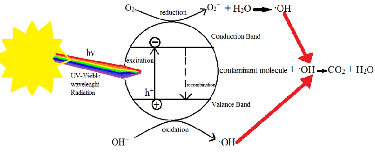
The basic principle of photocatalytical degradation mechanisms is that UV light upgrades electrons from the valance band to the conduction band, and holes and electrons will be separated. The holes and electrons reach the semiconductor-environment interface, and react with appropriate redox species in the semiconductor-environment. In that time, reactive species are arisen from the surrounding water by charge exchange at the valance band and at the conduction band as represented in Figure 2.2. These radicals and peroxide ions are able to virtually oxidize all organic materials to CO2 and H2O. Furthermore, at the valence band, direct h+ transfer to
adsorbed species to initiate decomposition may also be considered [70]. The reactions that are promoted with the absorption of photon (hυ) and photocatalytical degradation mechanism are given below.
8
Figure 2.2: Schematic illustration of the semiconductor materials when used for degradation contaminants in water under the sunlight.
Semiconductor (SC) + hυ → SC (e- + h+) (2.1)
SC e_ + O2→ SC + O2̄ (2.2)
O2̄ + H2O → SC + ·OH (2.3)
SC (h+) + OH ̄ → SC + ·OH (2.4) As a result of consecutive reaction highly reactive peroxide (O2̄ ) and hydroxyl
radical (·OH) attack the organic contaminants (OCs) on the surface leading to degradation.
OCs + ·OH → CO2 + H2O (2.5)
Thus optically illuminated photocatalyst semiconductor can degrade and mineralize organic compounds through a series of oxidation reactions.
2.1.2. Titanium dioxide
The element Titanium was discovered in 1791 by William Gregor, in England. Martin H. Klaproth was not able to make the pure element of titanium however he was only able to produce titanium dioxide (TiO2). TiO2 is a multifaceted compound.
It's the stuff that makes toothpaste white and paint opaque. TiO2 is also a potent
photocatalyst that can break down almost any organic compound when exposed to sunlight, and a number of companies are seeking to capitalize on TiO2's reactivity by
developing a wide range of environmentally beneficial products, including self- cleaning fabrics, auto body finishes, and ceramic tiles. TiO2 as a photocatalyst for
9
photocatalytic water splitting on TiO2 by Fujishima and Honda in 1972 [6]. Titanium
dioxide has long been regarded as an attractive photocatalyst, however, the use of titanium dioxide is impaired by its wide band gap (3.2-3.6 eV) [37],which requires ultraviolet (UV) irradiation for photocatalytic activation (λ <387 nm). As known, UV light accounts for only about 5 % of solar energy while visible light does 45 % [38]. The shift of the optical response of titanium dioxide from UV to the visible spectral range will have a profound positive effect on the efficient use of solar energy in photocatalytic reactions. Therefore, considerable efforts have focused on band-gap engineering of TiO2 by incorporating several atoms in to structure.Titanium dioxide
is a well-known photocatalyst for water and air treatment as well as for catalytic production of gases. The general scheme for the photocatalytic destruction of organics begins with its excitation by supra bandgap photons, and continues through redox reactions where OH radicals, formed on the photocatalyst surface, play a major role. Titanium dioxide is non-toxic and therefore is used in cosmetic products (sunscreens, lipsticks, body powder, soap, pearl essence pigments, tooth pastes) and also in special pharmaceutics. Titanium dioxide is even used in food stuffs, for instance in the wrapping of salami. Small amounts added to cigar tobacco are the cause of the white ash cigar smokers so cherish.
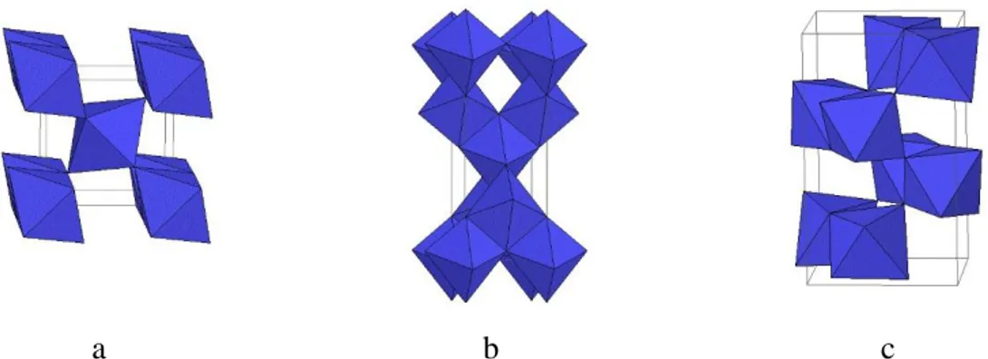
Titanium dioxide has three different main crystal structures; rutile (tetragonal, a=b=4.584 Å, c=2.953Å), anatase (tetragonal, a=b=3.782 Å, c=9.502 Å) and brookite (orthorhombic, a=9.166 Å, b=5.436 Å, c=5.135 Å) [71]. The two commonly available stable phases of TiO2 are rutile and anatase. These phases transitions begins
to appear at 280-480oC, 480-880oC for anatase phases and rutile phases, respectively [72]. Rutile structure is more stable about 1.2-2.8 kcal/mol than anatase structure. Rutile is preferred to anatase for optical and dielectric applications because of its high refractive index and dielectricity. Whereas, anatase is preferred for all applications related to photocatalytic activity due to its higher charge carrier mobility. The anatase phase is like pyramid structure and, it is stable at low temperatures. The crystals of rutile phase are needle-shaped structure and, this phase is formed at elevated temperatures. Both of rutile and anatase phases are used mostly as compared with brookite phase. The crystal lattice structures of rutile, anatase and brookite phases are showed in Figure 2.3.
10
Figure 2.3: Representation of the crystal lattice structures of TiO2 phases; a) rutile, b)
anatase, c) brookite [71].
Titanium dioxide is an n-type semiconductor having a band gap of 3.2 and 3.6 eV, respectively, for anatase and rutile phases. Electronic structure of TiO2 has been
determined experimentally by various groups [73]. The valence bands of TiO2 can be
split into three main regions: the σ bonding in the lower energy region mainly due to O-p σ bonds; the π bonding in the middle energy region; and O-p π states in the higher energy region due to O-p π nonbonding states where the hybridization with d states of titanium is almost negligible. The conduction band is split into titanium eg (>5 eV) and t2g bands (<5 eV). The dxy states of t2g are dominantly located at the
bottom of the conduction band. The rest of the t2g bands are anti-bonding with p states of oxygen. The main peaks of the t2g bands are identified to be constituted by mostly dyz and dzx states. The lowest empty energy levels are titanium dxy and thus
they are representative of the conduction band (CB) edge, whereas full O p states define the valence band (VB). The conductivity of TiO2 is mainly dependent upon
the presence of oxygen vacancies and Ti3+ cations, which makes TiO2 an n-type
semiconductor. Key point of the optical and electrical properties is the presence of defects that provide additional states in the bandgap near the CB or VB. When the semiconductor TiO2 absorbs photons with energy equal to or greater than its Eg, the
electrons in VB will be excited to CB, leaving the holes in VB. This electron−hole pair generation process in TiO2 can be expressed as follows:
TiO2 + hυ → e- (TiO2) + h+ (TiO2) (2.6)
In literature, there are various works about doping in titanium dioxide as listed in Table 2.1. Macak et al reported nitrogen (N) doping of self-organized titanium dioxide nano-tubular layers in 2006 [39]. After year, Li et al doped copper (Cu) in titanium dioxide nanotube array [53], Yang et al studied at co-doping with carbon (C) and vanadium (V) of titanium dioxide nanotube arrays [52], and Chen et al tried
11
to make carbon (C) and nitrogen (N) co-doped titanium dioxide and reported N atoms could incorporate into the lattice of anatase through substituting the sites of oxygen atoms, while most C atoms could form complex carbonate species at the surface of titanium dioxide nanoparticles [74]. In 2008, Su et al doped boron in titanium dioxide nanotube array and Zhang et al demonstrated the synthesis of P-doped TiO2 NTs with uniform [41, 55]. In recent years, tungsten (W) and nitrogen
(N) doped titanium dioxide nanotube arrays, molybdenum (Mo) and nitrogen co-doped titanium dioxide nanotube arrays, silver (Ag) co-doped titanium dioxide nano-materials, and in addition to these, molybdenum, antimon (Sb) and sulphide (S) tridoped titanium dioxide nano-particles were fabricated by researchers [38, 42, 49, 51].
12
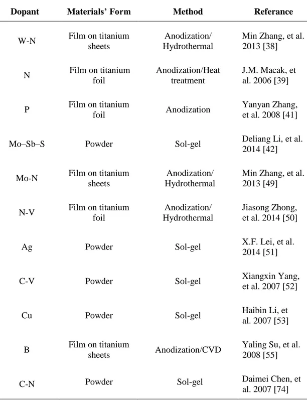
Table 2.1: Some studies in literature based on doped titanium dioxide.
Dopant Materials’ Form Method Referance
W-N Film on titanium sheets
Anodization/ Hydrothermal
Min Zhang, et al. 2013 [38] N Film on titanium foil Anodization/Heat treatment J.M. Macak, et al. 2006 [39] P Film on titanium foil Anodization Yanyan Zhang, et al. 2008 [41]
Mo–Sb–S Powder Sol-gel Deliang Li, et al.
2014 [42]
Mo-N Film on titanium sheets
Anodization/ Hydrothermal
Min Zhang, et al. 2013 [49] N-V Film on titanium foil Anodization/ Hydrothermal Jiasong Zhong, et al. 2014 [50]
Ag Powder Sol-gel X.F. Lei, et al.
2014 [51]
C-V Powder Sol-gel Xiangxin Yang,
et al. 2007 [52]
Cu Powder Sol-gel Haibin Li, et al. 2007 [53]
B Film on titanium
sheets Anodization/CVD
Yaling Su, et al. 2008 [55]
C-N Powder Sol-gel Daimei Chen, et
13 2.2. Electrochemical Anodization
2.2.1. Basics of anodization
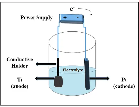
Anodization is an electrochemical passivation process, which is applied to some metallic materials (Ti, Zn, Al and etc.) having their own natural oxide layers. As in all electrochemical interactions, reduction and oxidation (redox) reactions also occur in anodization processes. Redox reaction is a type of chemical interaction that involves a transfer of electrons between two species. Since all types of chemical bonding are related to electrons’ motion, all of chemical reactions are fundamentally electrical interactions. In addition to that, electrochemical studies provide to understand and make systematic to redox reactions. A schematic anodization cell in which these reactions take place is illustrated in Figure 3.1.
Figure 2.4 : Schematic illustration of anodization process
Basically, an electrochemical process is indicated by anode and cathode reactions as follows;
Anode: 2H2O→O2(g)+4H++ 4ē (3.1)
Cathode:2ē+2H2O→H2(g)+2OH̄ (3.2)
However, anode reaction of the anodization process forms metal oxide on the metal surface through electrolysis. When metal are exposed to a adequately anodic voltage in an electrolytic cell (as in Figure 3.1.a), an oxidation reaction M → M˟+ + xē will
14
be started. On the basis of electrolyte and specific anodization parameters, constitutively three possibility states: I) The M˟+ ions are solvated in the electrolyte;
II) the M˟+ ions react with oxygen ions (O2-) which provided by H
2O in the
electrolyte and form an ordered oxide (MO) layer if MO is not solvable in the electrolyte; III) under some electrochemical conditions, both solvation and oxide formation get into competition leading to porous MO [75]. Under determined experimental conditions, growth of porous oxide can take place [76]. Furthermore, under some specific conditions, growth of TiO2 nanotube arrays or formation of thick
self-organized mesoporous layers can be observed [33-36, 77]. 2.2.2. Anodization of titanium
Anodization of titanium is an electrolytic process that creates a protective or decorative oxide film over a metallic titanium surface. Anodization typically increases both the thickness and density of the oxide layer that forms on metal surface exposed to ambient conditions. In order that, the metallic titanium is connected to the positive terminal of a direct current power supply and placed in an electrolytic bath where it serves as the anode (as in Figure 2.1). The cathode is commonly a plate or rod of platinum, although materials such as carbon are sometimes used. In the process, migration of electrons occurs, but is also necessary for oxygen ions (O2-) and M2+ ions to be combined. Basically, at the interface;
oxygen atoms add two electrons to become oxide ions, at the surface of the metal; metal atoms are oxidized to metal ion by losing electrons. When power (electrical potential) is applied, electrons are forced from the electrolyte to the positive anode. It provides to leaved surface metal atoms exposed to oxygen ions (O2-) within the electrolyte. The atoms react and become an in situ integral part of the oxide layer. The electrons travel through the power source and return to the cathode where, if an appropriate electrolyte pH is present, they react with hydrogen ions and the combination bubbles off as hydrogen gas. Since the metal oxide partially dissolves in any electrolyte, it is necessary to use only those electrolytes for which the oxide forms more rapidly than it dissolves. The electrolyte composition is important for the production of either porous oxide surface or flat barrier oxide surface. Oxide barrier layers grow in those neutral or slightly alkaline solutions in which titanium dioxide is generally insoluble. Porous oxide layers grow in acidic electrolytes with fluoride [76]
15
in which oxide forms rapidly dissolves without current supplying. The acid cations also affect the resulting nanotube array structures. Fabrication of TNTAs via anodic oxidation of Ti was first reported in 2001, and later studies focused on accurate control and extension of the nanotube morphology, length and pore size, and wall thickness [78].
TiO2 nanotube arrays synthesis can be made by using aqueous, buffered, polar
organic or non-fluorid based electrolytes [78]. In literature, used aqueous electrolytes; these are HF (hydrofluoric acid), HNO3/HF (nitric acid/hydrofluoric
acid mix), H2SO4/HF (sulfuric acid/hydrofluoric acid mix), H2Cr2O7/HF (dichromic
acid/hydrofluoric acid mix), CH3COOH/NH4F (acetic acid/ammonium fluoride mix),
H2SO4/NH4F (sulfuric acid/ammonium flouride mix), H3PO4/HF (phosphoric
acid/hydrofluoric acid mix), H3PO4/NH4F (phosphoric acid/hydrofluoric acid mix)
containing electrolytes. As an example of buffered electrolytes are KF (potassium fluoride) or NaF (sodium fluoride) / NaOH (sodium hydroxide) / H2SO4, NaHSO4
(sulfuric acid, sodium hydrogen sulphate) or C6H8O7 (citric acid) containing
solutions. Species of electrolytes; these are formamide (CH3NO), dimethly
formamide (C3H7NO), dimethly sulfoxide (C2H6OS;DMSO), ethylene glycol
(C2H6O2), diethylene glycol (C4H10O3), methanol/water/hyrogenfluoride
(CH4/H2O/HF) electrolytes used to produce formation of longer nanotubes [60]. In
addition to these, non-fluoride based electrolytes are used for TNTAs. By using titanium foil as anode and copper as cathode in HCl (hydrogen chloride) electrolyte solutions, TNTAs were formed [61]. Another electrolyte is consist of H2O2
(hydrogen peroxide) aqueous or HCl/ H2O2 solution [79].
Mechanism of TNTAs formation by anodization is clarified by key points of the process that are: (1) oxide growth at the metal surface due to interaction of the metal with O2– or OH-ions. After formation of an initial oxide layer, these anions migrate through the oxide layer reaching the metal/oxide interface where they react with the metal. (2) Metal ion (Ti4+) migration from the metal at the metal/oxide interface; Ti4+ cations will be discharged from the metal/oxide interface under application of an electric field that move toward the oxide/electrolyte interface. (3) Due to the applied electric field the Ti–O bond undergoes polarization and is weakened dissolution of the metal cations. Ti4+ cations dissolve into the electrolyte, and the free O2– anions move to the metal/oxide interface, process (1), to interact with the metal.
16
(4) Chemical dissolution of the metal, or oxide, by the acidic electrolyte. Chemical dissolution of TiO2 in the HF electrolyte and applying voltage play a critical role in
the formation of nanotubes rather than simple nanoporous structures [79]. In the HF based aqueous electrolyte, reactions become as below;
4HF(aq)→ 4H+(aq) + 4F-(aq) (3.3)
4H2O(aq)→ 4H+(aq) + 4OH-(aq) (3.4)
4F-(aq) + 4OH-(aq) → 4O2–(aq) + 4HF(aq) (3.5)
Ti(s) + 4H+(aq) + 4F-(aq)→ Ti4+(aq) + 4F-(aq) + 2H2(g) (3.6)
By the anodization started, the initial oxide layer formed due to interaction of the surface Ti4+ ions with oxygen ions (O2–) in the electrolyte [79]. Reaction of oxide layer formation at the anode is as follows;
Ti4+(aq) + O2–(aq) → TiO2(s.c.) (3.7)
At the cathode, hydrogen gases occur as below reaction;
8H+(aq) + 8e- → 4H2(g) (3.8)
However, fluorine ions can attack the oxide layer if intensity of HF in the electrolyte is unnecessary, or the ions being mobile in the anodic layer under the applied electric field react with Ti4+ as follows;
TiO2(s.c.)+6F-+4H+→(TiF6)2-(aq)+2H2O (3.9)
Ti4+
(aq)+6F-→ (TiF6 )2-(aq) (3.10)
As a result of that, tetra fluoro titanate complex anions can be formed in electrolyte and it can be an obstacle to formation of nanotube arrays.
2.2.3. Doping into titanium dioxide nanotube layer by anodization
Semiconducting doping, namely band-gap engineering, is creating a secondary electronically active species into the lattice. The most typical methods to prepare doped TiO2 nanostructures are: 1) treating growed TiO2 nanomaterials in a solution
or melt of the doping species; 2) thermal treatments in dopant rich gas atmospheres; 3) production of nanomaterials by sputtering in an atmosphere of dopant; 4) high-energy ion implantation; and 5) anodization in an electrolyte containing dopant solution [70].
17
In recent years, anodization processes have been used greatly to produce doped TiO2
nanotube arrays. To accomplish it, different dopants as B (boron)[59], Nb (niobium) [80] added in fluoride based electrolyte.
In this study, B-doped TiO2 nanotube arrays were fabricated by anodization process according to below mechanism created by predicted possible electrochemical reactions;
HF(aq) → H+(aq) + F-(aq) (3.11)
C2O4H2.2H2O(k) + H2O(aq)→ C2O42-(aq) + 5H+(aq) + 3OH-(aq) (3.12)
NaBF4 (aq) + H2O(aq)↔ Na+(aq) + BF4̄ (aq) + H+(aq) + OH-(aq) (3.13)
H2O(aq)↔H+(aq) + OH-(aq) (3.14)
These reactions explain to components of electrolyte before apply current to anodization system. After apply current;
Anode reaction as follows,
F-(aq)+BF4̄(aq)+C2O42-(aq)+OH-(aq)↔BF3(aq)+C2F6(aq)+O2(g)+O2-(aq)+H+(aq)+F-(aq) (3.15)
Ti4+(aq) + O2–(aq)→ TiO2(s.c.) (3.16)
Ti3+(aq) + BF4̄ (aq) + O2–(aq)→ TiBF4O(s.c) (3.17)
Ti4+
19 3. EXPERIMENTAL SECTION
3.1. Materials
Titanium (Grade 2, TiMET Metal & Medical Co.) cylinders with 15mm diameter and 10 mm thickness were used as substrates to form TNTAs.Hydrogen floride (HF, 40,0%, Sigma-Aldrich), oxalic acid dihydrate (C2O4H2.2H2O, ≥99,0%
Sigma-Aldrich), nitric acid (HNO3, ≥65% Sigma-Aldrich) sodium tetra-fluoro-borate
(NaBF4, 97,0+% Sigma-Aldrich), acetone (C3H6O, Sigma-Aldrich) and ethyl alcohol
(C2H6O, Sigma-Aldrich) were used in production process of TNTAs. Methylene blue
(C16H18ClN3S, Sigma-Aldrich) was used for photocatalytic degradation tests. All of
the chemicals were analytical grade and all experiments were carried out at room temperature using distilled water.
3.2. Method
3.2.1. Preparation of titanium substrates
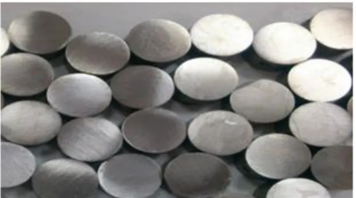
The purchased 15mm diameter titanium rod was cut into cylinders as substrates with 10mm-height via sample cutting device (Struers, Lobotom 5). Subsequent to cutting process, substrates were sequentially grinded by 80-2000 grit emery papers. Grinded substrates were cleaned in acetone, ethyl alcohol and pure water containing solutions by an ultrasonic bath. Finally, the substrates with enhanced surfaces were obtained as seen in Figure 3. 1.
20
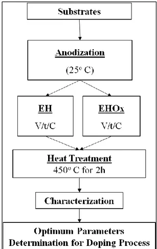
3.2.2. Fabrication and optimization of titanium dioxide nanotube arrays
In this study, fabrication of TNTAs were provided via electrochemical anodization in two different electrolytes defined as EH and EHOx. Electrolyte EH and EHOx included HF/H2O and C2H2O4·2H2O/HF/H2O respectively. Effects of anodization
parameters (working voltages; V, processing times; t and HF concentrations; C) on surface morphologies of anodized structures were evaluated to determine optimum conditions for boron incorporation. The production flowchart for these processes is represented in Figure 3.2. According to the flowchart sample and code designation for anodization in EH and EHOx electrolytes were listed in table 3.1 and table 3.2 respectively. Herein, temperature for heat treatment was chosen according to literature [72].
21
Table 3.1: Samples anodized in EH.
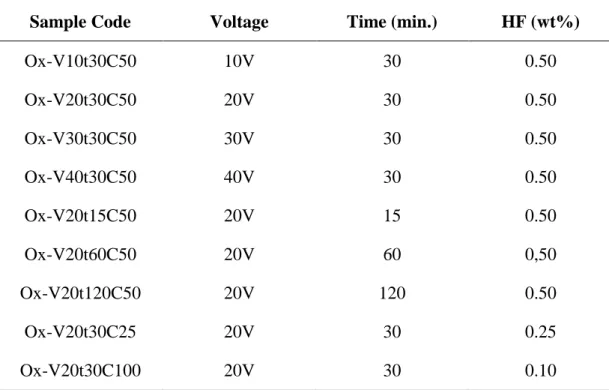
Sample Code Voltage Time (min.) HF (wt%)
V10t30C50 10V 30 0.50 V20t30C50 20V 30 0.50 V30t30C50 30V 30 0.50 V40t30C50 40V 30 0.50 V20t15C50 20V 15 0.50 V20t60C50 20V 60 0.50 V20t120C50 20V 120 0.50 V20t30C25 20V 30 0.25 V20t30C100 20V 30 0.10
Table 3.2: Samples anodized in EHOx.
Sample Code Voltage Time (min.) HF (wt%)
Ox-V10t30C50 10V 30 0.50 Ox-V20t30C50 20V 30 0.50 Ox-V30t30C50 30V 30 0.50 Ox-V40t30C50 40V 30 0.50 Ox-V20t15C50 20V 15 0.50 Ox-V20t60C50 20V 60 0,50 Ox-V20t120C50 20V 120 0.50 Ox-V20t30C25 20V 30 0.25 Ox-V20t30C100 20V 30 0.10
The optimum anodization parameters were determined via SEM observations by determining the homogenous, smooth and uniform morphologies (see: 4.2.1. TiO2
22
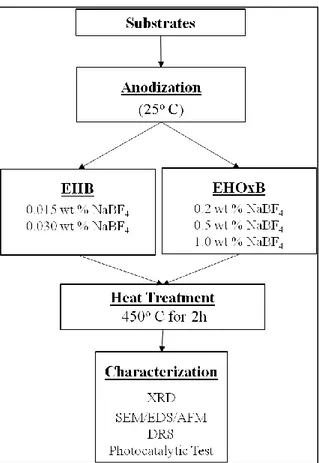
3.2.3. Fabrication of boron doped titanium dioxide nanotube arrays
Based on the obtained results in prior anodization experiments, electrolytes EH and EHOx with optimized HF content were modified with sodium tetra fluoro borate as a chemical agent to provide boron incorporation. Hence the designations of the new electrolytes were defined as EHB and EHOxB to cite modified electrolytes EH and EHOx respectively. The contents of EHB and EHOxB consisted of HF/H2O/NaBF4
and C2H2O4·2H2O/HF/H2O/NaBF4 respectively. Furthermore anodization processes
were conducted with various concentrations of sodium tetra fluoro borate (0.015 and 0.030 wt% for EHB and 0.2, 0.5 and 1.0 wt % for EHOxB) for both electrolytes. Code-designations and processing parameters of the boron incorporated samples which were anodized in electrolytes EHB and EHOxB as listed in table 3.3 and table 3.4 respectively. Finally the samples were annealed at 450oC for 2 hours in order to obtain crystalline anatase structure. Annealed samples were characterized with phase analysis (XRD), micro structural analysis (SEM/EDS/AFM), optical analysis (DRS) and photocatalytic test as outlined the flowchart in Figure 3.3.
23
Figure 3.3: Flowchart of production and characterization of doped TNTAs. Table 3.3: Samples anodized in EHB.
Sample Code NaBF4 Concentration (wt%) Time (min.) Voltage HF (wt %) B015-V20t120C50 0.015 120 20V 0.5 B030-V20t120C50 0.030 120 20V 0.5
Table 3.4: Samples anodized in EHOxB.
Sample Code Dopant Concentration (wt %) Time (min.) Voltage HF (wt %) B2-Ox-V20t120C50 0.2 120 20V 0.5 B5-Ox-V20t120C50 0.5 120 20V 0.5 B10-Ox-V20t120C50 1.0 120 20V 0.5
24 3.2.4. Structural Characterization
X-ray diffraction (XRD) is one of the primary techniques to analyze all kinds of materials such as powders and crystals. XRD can provide information about crystalline structure and structural phases.
Measurements were performed by means of XRD with a grazing angle attachment and an incident angle of 1° (Rigaku, D/Max-2200/PC). X-Ray radiation of CuKα was set at 40 kV and 36 mA with a scanning speed of 4° 2θ/min, from 3° to 90°. 3.2.5. Morphological and Nanostructural Characterization
The Scanning Electron Microscope (SEM) is a versatile electron microscope that images a sample by scanning it with a high-energy beam of electrons in a raster scan pattern. In Typical SEM configuration, electrons are thermo ionic emitted from a tungsten or LaB6 cathode filament towards an anode. The electron beam, with a typical energy ranging from a few KeV to 30 KeV, is focused by successive lenses in a beam with a very fine spot size. When the beam introduces with the surface, different kind of electrons can be detected. The types of signals produced by an SEM include secondary electrons (SE), back-scattered electrons (BSE) and characteristic X-rays.
In this study, the surfaces of TiO2/doped TiO2 were examined by using JEOL
JSM-7600F instrument operating at an accelerating voltage of 5.0 kV with several magnifications.
The atomic force microscope (AFM) is one kind of scanning probe microscopes (SPM). SPMs are designed to measure local properties, such as height, friction, magnetism, with a probe. To acquire an image, the SPM raster scans the probe over a small area of the sample, measuring the local property simultaneously. Using an atomic-force microscope (AFM), it is possible to measure a roughness of a sample surface at a high resolution, to distinguish a sample based on its mechanical properties (for example, hardness and roughness) and, in addition, to perform a micro fabrication of a sample (for example, an atomic manipulation). Figure 3.4 illustrates basically working princible of AFM.
In this study, 62,0x62,0 µm region at surfaces of doped TNTAs were scanned by using AFM (NanoSurf Flex AFM )operates with 256 lines.
25
Figure 3.4: Typical configuration of AFM is illustrated [83]. 3.2.6. Optical characterization
Optical characterization can be appointed by measuring of band gap energy. The measurement of the band gap of materials is important in the semiconductor and solar industries. The term “band gap” refers to the energy difference between the top of the valence band to the bottom of the conduction band; electrons are able to jump from one band to another. An electron is in need a specific minimum amount of energy to jump from a valence band to a conduction band. Mentioned energy is called the band gap energy. A diagram illustrating the bandgap is shown in Figure 3. 5.
26
The band gap energy can be calculated by equation is E=ħc/λ. Example of this calculation is given at table 3. 4. As a result of this calculations, equation is Eq. (3.1) E = 1240/λ find directly to band gap energy value [85, 86]. Value of λ is cut off wavelength value which can be determined by wavelength to absorbance diagram from diffuse reflectance spectroscopy (DRS). Principle of DRS is schematized in Figure 3.6.
Table 3.5: Calculations of band gap energy [85, 86]. Band Gap Energy (E) = h*c/λ
ħ= Planks constant = 6.626 x 10⁻³⁴ Joules sec
c = Speed of light = 3.0 x 10⁸ meter/sec λ = Cut off wavelength = 410.57 x 10⁻⁹ meters
ħ c λ E eV
6.63E-34 3.00E+08 4.11E-07 4.84156E-19 3.025976
Where 1eV = 1.6 X 10⁻¹⁹ Joules (conversion factor)
Figure 3.6: Illustration of DRS principle [87].
In this study, reflectance of undoped samples and doped samples were measured by Evolution 600 UV-Vis Thermo Scientific DRS device. Values of reflectance were converted by program driving to DRS device. The wavelength absorbance diagrams of these samples were drawn and the cut off wavelength was determined for all samples, therefore, the band gap energy was calculated accordingly mentioned calculations.
27 3.2.7. Photocatalytical Characterization
Aqueous methylene blue (MB) solutions are mostly employed artificial impurities in literature so as to evaluate the photocatalytic activity of the catalysts [38, 42, 46, 74, 76, 81, 84]. MB was first prepared in 1876 by German chemist Heinrich Caro from methyl-aniline. Methylene blue is an organic compound which is heterocyclic aromatic with the chemical formula C16H18N3SCl. MB aqueous solution (MB+) is a
cationic dye with maximum absorption of light around 664 nm [88]. With this manner, to determine the photocatalytic degradation performance and kinetics of the TNTAs, Lambert-Beer correlation curve is plotted, and a linear relation between absorbance (A) and concentration (C) is identified by this way [89].
Lambert-Beer correlation curve is derived by Lambert-Beer equation which is expressed as; Eq. (3.2) 𝐴 = 𝐴𝑏𝑠𝑜𝑟𝑏𝑎𝑛𝑐𝑒 = log I0 / I = Є. L. C. In the expression A, I0, I, Є, L and C denote absorbency, initial light intensity, light intensity, coefficient
of absorbency, light path and concentration respectively. This linear relationship between A and C is valid under some conditions; monochromatic ray, homogenous sample and < 0.01 molarity. In more concentrated solutions refractive index will increase and interaction of molecules will be effective (A-C the linear relationship is broken). As a result of these, the linear correlation curve was plotted through the samples with concentration 0 to 1x10⁻⁵M lower concentrated sample (Figure 3.7).
0.0 2.0x10⁻⁶ 4.0x10⁻⁶ 6.0x10⁻⁶ 8.0x10⁻⁶ 1.0x10⁻⁵ 0.0 0.1 0.2 0.3 0.4 0.5 0.6 0.7 0.8 y=76077.84x R2=0,9987 Experimental Data Linear Fit Absor ba nc e Concentration (mol/L) Figure 3.7: Absorbance-Concentration (mol/L) correlation plot
28
Subsequent to derivation of the absorbance and concentration relation of aqueous MB solutions, the photocatalytical activity tests for both TNTA and B-TNTA samples were conducted by immersing samples in to beakers containing 25ml of 0.25x10⁻⁵ M methylene blue solutions. In order to record catalyst-free degradation of MB an arbitration solution was also prepared. The degradation reactions were performed by exposing the samples to the UV irradiation with a light source (Osram Uv Vitalux 300 W/m2) in a photocatalytic reactor depicted in Figure 3.8. To prevent the evaporation of the MB solutions, a transparent glass cap was placed above the beaker and water cooling system was used around the beakers (Figure 3.8). The degradation efficiencies are calculated by using absorbance values at 664nm obtained from UV-Vis spectrophotometer (UV mini-1240 UV-Vis/Shimadzu) in different intervals.
Figure 3.8: System of UV simulator and photocatalytic experiment setup illustrated schematically.
Furthermore the recorded absorbencies of the samples were converted to concentrations for different intervals. Using the concentrations, the degradation efficiencies and the reaction kinetics of the samples were calculated, in order to point out the effect of boron incorporation on the photocatalytical properties of the TNTA.
29 4. RESULTS AND DISCUSSION
Production and characterization of titanium dioxide nanotube structures and boron incorporation studies were sequentially performed in this research. Therefore, in this section of the thesis; phase structure, nanostructure, surface morphology, band gap measurements and photocatalytical properties of the samples will be presented in accordance with literature.
4.1. Phase Analysis
Crystalline structure and phases of the samples were determined by examining the x-ray diffraction patterns. The XRD patterns of the samples anodized in electrolyte EHB (V20T120C50, B125-V20T120C50, B25-V20T120C50) and EHOxB (Ox-V20T120C50, B2-Ox-(Ox-V20T120C50, B5-Ox-(Ox-V20T120C50, B10-Ox-V20T120C50) were represented in Figure 4.1 and Figure 4.2, respectively. According to the results it can be stated that all of the patterns are including two crystalline phases. These phases are anatase TiO2 (JCPDS 021-1272) and titanium (JCPDS 044-1294) which
belong to TNTAs and titanium substrates, respectively. Dominant diffraction peaks at 2θ= 35o, 40o correspond to metallic titanium substrate for all samples. Other
characteristic peaks at 2θ= 25.2o; 37o; 37.9o and 38.5o were observed for both TNTA
and B-TNTA structure corresponding to anatase TiO2. It can be inferred that; as a
result of the sequental anodization and heat treatment, production of photocatalytically active anatase phase was succesfuly obtained for all samples. In addition, it can be expressed the intense peaks of titanium substrates were obtained owing to low thicknesses of anodized layers. Since the diffraction characteristics are similar for all samples, patterns for the samples anodized in EH and EHOx (except V20T120C50 and Ox-V20T120C50 ) was not presented in this title.
30 0 20 40 60 80 0 50 100 150 0 50 100 150 0 5 10 15 200 20 40 60 80 1 1 2 2 1 1 B030-V20T120C50 Intensity two-theta (degree) 1 1 2 1 2 1 B015-V20T120C50 2 2 1 1 1 1 1 : Metallic Titanium (044-1294) 2 : Anatase (021-1272) V20T120C50
Figure 4.1: XRD patterns of the samples anodized in electrolyte EHB.
0 20 40 60 80 0 5 10 0 50 100 150 0 50 100 1500 50 100 150 0 20 40 60 80 2 2 1 1 B2-Ox-V20T120C50 Intensity two-theta (degree) 2 1 1 1 1 B5-Ox-V20T120C50 2 1 1 1 1 B10-Ox-V20T120C50 1 : Metallic Titanium (044-1294) 2 : Anatase (021-1272) 2 1 1 1 1 Ox-V20T120C50
Figure 4.2: XRD patterns of the samples anodized in electrolyte EHOxB.
Obtained XRD patterns were found to be in a good agreement with the literature which are focused on the production of TNTAs [92-96]. In addition, it can be expressed that, obtained XRD results are similar with Na Lu [59] and Yaling Su [55, 58] who produced B-TNTA with different approaches. In addition any shift in the diffraction patterns were not observed as result of boron incorporation. As expressed by Na Lu [59] and Yaling Su [55, 58] the lower boron content make it hard to detect by XRD. Regarding to this, the boron contents in the structures were determined by energy-dispersive X-ray spectroscopy measurements in section 4.2.
31 4.2. Nanostructure Analysis
4.2.1. Titanium dioxide nanotube arrays
Surface morphology and structure of a catalyst is important for further photocatalytic tests. As mentioned elsewhere, the samples for the determination of optimum anodization parameters were produced in electrolyte EH and EHOx. The SEM images of these samples for various parameters were represented in Figure 4.3, 4.5, 4.7, and 4.4, 4.6, 4.8, for electrolyte EH and EHOx, respectively.
The SEM images of the samples anodized with anodization voltages 10V, 20V, 30V and 40V in electrolyte EH and electrolyte EHOx including 0.5wt% HF at 30 min were shown in Figure 4.3 and Figure 4.4. According to the figures, it can be expressed that formation of uniform and homogenously distributed TNTAs were occurred with sample anodized with 20V in electrolyte EH and EHOx.
32
Figure 4.3: SEM images of samples produced in electrolyte EH including 0.5 wt% HF a, b) 10V, c, d) 20V, e, f) 30V, g, h) 40V.
c
d
f
a
b
e
g
h
33
Figure 4.4: SEM images of samples produced in electrolyte EHOx including 0.5wt% HF. a, b) 10 V, c, d) 20 V, e, f) 30 V, g, h) 40 V.
a
b
c
d
f
g
h
e
34
In literature, Gong et al fabricated titanium dioxide nanotube arrays on titanium foil with voltages of 3, 5, 10 and 20V with anodizing time from 15-45 min. They observed that film morphology is nanoporous with pore sizes from 15 to 35 nm at low voltages. Discrete and cylindrical tube began to appear at voltages higher than 10V [29]. However, Erol et al reported a study about the effect of anodization parameters on the formation of nanoporous titanium dioxide layers. They worked to anodize at 20 oC for 30 min. at different voltages; 20, 30, 40, 50V and their results indicated that the formation of nanoporous structure was obtained by applying 20V similar to our results [81].
The SEM images of the samples anodized in electrolyte EH and EHOx including 0.25, 0.50 and 1.0 wt% HF with 20V at 30 min were shown in Figure 4.5 and Figure 4.6, respectively. According to the figures, it can be stated that uniform TNTAs were formed in both electrolyte EH and EHOx including 0.25 and 0.50 wt% HF.
35
Figure 4.5: SEM images of samples produced in electrolyte EH with various HF content (wt%); a, b) 0.25; c, d) 0.5; e, f) 1,0 with 20V.
b
c
d
e
f
36
Figure 4.6: SEM images of samples produced in electrolyte EHOx with various HF content (wt%); a, b) 0.25; c, d) 0.5; e, f) 1,0 with 20V.
In literature, Dikici et al reported that they obtained titanium dioxide nano-pore by anodization process using 1.0 wt% HF electrolyte with applying 20V at 30 min [90]. However, in this study, we could not observe these structure as seen at SEM images (in Figure 4.5e,f) of sample produced by the similar conditions, using electrolyte EH. But the observation of the porous structures was provided with sample anodized in electrolyte EHOx including 1.0wt% HF according to SEM images in Figure 4.6 e, f.
a
b
c
d
37
The SEM images of sample produced in electrolyte EH and EHOx including 0.5wt% HF with 20V at 15, 30, 60, 120 min were shown in Figure 4.7 and Figure 4.8. According to Figure 4.7, formation of uniform TNTAs (samples anodized in electrolyte EH for 15, 30, 60 and 120 min) was obtained.
38
Figure 4.7: SEM images of samples produced in electrolyte EH including 0.5 wt% HF a, b) 15 min, c, d) 30 min, e, f) 60 min, g, h) 120 min with 20V.
a
b
c
d
e
f
39
Figure 4.8: SEM images of samples produced in electrolyte EHOx including 0.5wt% HF at; a, b) 15 min, c, d) 30 min, e, f) 60 min, g, h) 120 min with 20V.
![Figure 2.1: Schematic illustration of the formation of photocatalytic reaction belonging to both man-made nano TiO2 catalysts and natural chlorophyll catalysts [69]](https://thumb-eu.123doks.com/thumbv2/9libnet/3711015.24955/31.892.198.769.372.661/schematic-illustration-formation-photocatalytic-belonging-catalysts-chlorophyll-catalysts.webp)
![Figure 3.4: Typical configuration of AFM is illustrated [83]. 3.2.6. Optical characterization](https://thumb-eu.123doks.com/thumbv2/9libnet/3711015.24955/49.892.315.662.166.383/figure-typical-configuration-afm-illustrated-optical-characterization.webp)
