■ я е д ?
JH.· ' 3·ν% .', ■■■ч...»·,■;> ", Λς .· ίϋί^.Φ .· ■ ' ι» ·ή
ü ·, ; ^ •'W ' I « .«М ьім''Ч ’м^кМкТм îM<U А«И'',іміі ,1^ '-'aé'.Will* ·ί»Μ| ЛМ «\>К
•^''ч 4 .-.·♦,<. .,,?\.··Κ',ν·.
PHYSICS AND APPLICATIONS OF PHOTONIC CRYSTALS
A DISSERTATION
SUBMITTED TO THE DEPARTMENT OF PHYSICS AND THE INSTITUTE OF ENGINEERING AND SCIENCE
OF BILKENT UNIVERSITY
IN PARTIAL FULFILLMENT OF THE REQUIREMENTS FOR THE DEGREE OF
DOCTOR OF PHILOSOPHY
By
Burak Temelkuran
April, 2000
®c
I certify that I have read this thesis and that in my opinion it is fully adequate, in scope and in quality, as a dissertation for the degree of Doctor of Philosophy.
ILWL
Assoc. Prof. Ekmel (Supervisor)
I certify that I have read this thesis and that in my opinion it is fully adequate, in scope and in quality, as a dissertation for the degree of Doctor of Philosophy.
Prof. Alexander Shumovsky.
I certify that I have read this thesis and that in my opinion it is fully adequate, in scope and in quality, as a dissertation for the degree of Doctor of Philosophy.
I certify th at I have read this thesis and th at in my opinion it is fully adequate, in scope and in quality, as a dissertation for the degree of Doctor of Philosophy.
Asst. Prof. Ahmet Oral
I certify that I have read this thesis and that in my opinion it is fully adequate, in scope and in quality, as a dissertation for the degree of Doctor of Philosophy.
Serdar Ozçelik
Approved for the Institute of Engineering and Science:
Prof. Mehmet Bar
ABSTRACT
PHYSICS AND APPLICATIONS OF PHOTONIC CRYSTALS
Burak Temelkuran
Ph. D. in Physics
Supervisor: Assoc. Prof. Ekmel Ozbay
April 2000
We first fabricated a dielectric based layer-by-layer photonic crystal, with a three-dimensional photonic band gap at microwave frequencies. We investigated the transmission, reflection and defect characteristics of the crystal. A Fabry-Perot cavity analogy was used to understand the localization of the electromagnetic (EM) fields around defects. We then showed the enhancement of the EM held within the defect volumes, and suggested a possible application: resonant cavity enhanced detectors built around photonic crystals. We demonstrated that a detector inserted inside the defect volume benefits from the frequency selectivity and the highly enhanced field of the cavity. Next, we investigated the radiation of the EM fields from a source inserted in the defect volume, and observed that the radiated field has a very high directivity and efficiency. The experimental results agreed well with the theoretical expectations.
We demonstrated waveguiding structures built around photonic crystals. We showed that EM waves could be guided through a planar air gap between two photonic crystals, in which the wave is coupled inside the defect volume, and having no where else to go, propagates through this opening. The dispersion diagrams for these planar waveguide structures also agreed well with the theoretical expectations of our waveguide model. We also showed that, the wave could be guided along a single missing rod, and demonstrated the bending of the EM waves for these waveguide structures with “L” shaped openings.
We tested metallic photonic crystals built in different dimensions and diflferent filling ratios. We observed many superiorities of these structures when compared to dielectric-based photonic crystals. A full characterisation of various metallic photonic crystals was performed. We also showed th at metallic photonic crystals are suitable for some of the applications we have demonstrated for dielectric structures. We also fabricated a new layer-by-layer photonic crystal using highly doped silicon wafers processed by semiconductor micromachining techniques, with a band gap at millimeter wave frequencies. We showed that the transmission and defect characteristics of these structures are analogous to metallic photonic crystals, as we have predicted. The experimental results agree well with the predictions of the transfer matrix method (TMM) simulations. The method can be extended to fabricate these crystals at THz. frequencies.
K eyw ords: Photonic Crystal, Photonic Band Gap (PBG), Defect, Fabry- Perot Cavity, Resonant Cavity Enhancement, EM Field Radiation, Directivity, Waveguide, Transfer Matrix Method (TMM), Doping, Semiconductor Micromachining.
ÖZET
FOTONİK KRİSTALLERİN FİZİĞİ VE UYGULAMALARI
Burak Temelkuran
Fizik Doktora
Tez Yöneticisi: Doç. Dr. Ekmel Özbay
Nisan 2000
Katmanlardan oluşan ve mikrodalga frekanslarında üç boyutlu fotonik bant aralığı gösteren bir fotonik kristal ürettik. Bu kristalin geçirgenlik, yansıtma ve düzensizlik özelliklerini inceledik. Fabry-Perot modeli benzetmesi kullanarak bu düzensizliklerde elektromanyetik dalgaların lokalize oluşunu açıkladık. Daha sonra yaratılan bu düzensizliklerin oluşturduğu boşluklarda elektromanyetik (EM) dalganın yükseltgendiğini göstererek olası bir uygulama önerdik: Fotonik kristallerde yaratılan rezonans kavite tarafından yükseltgenmiş detektörler. Düzensizlik içine yerleştirilen detektörün, bu kavitenin frekans seçiciliğinden ve kavite içindeki yükseltgenmiş alandan faydalandığını gösterdik. Bu tür düzensizliklerin içine yerleştirilen bir kaynaktan yayılan EM dalganin belirli bir yönde ve yükseltgenmiş alduğunu gözlemledik. Kuramsal ve deneysel sonuçların uyduğunu gördük.
Fotonik kristalleri kullanarak dalga kılavuzu yapmak için bazı önerilerde bulunduk. İki fotonik kristal arasında düzlemsel boşluk sayesinde, böyle bir düzensizliğe giren bir dalganın, gidecek başka bir yeri olmadığı için bu açıklık boyunca ilerlediğini gösterdik. Deneysel olarak bulduğumuz dalga vektörünün frekansa bağlı değişimi dalga kılavuzu modelimizin kuramsal sonuçlarıyla uyuştu. Bundan başka, dalganın fotonik kristalden çıkarılan bir çubuk boyunca da kayıp olmadan ilerlediğini gözlemledik ve bu dalga
kılavuzu yapılarıyla dalganın “L” şeklinde bir boşluktan kayıp olmaksızın dönebildiğini gösterdik.
Boyutları ve doluluk oranları değişik bazı metalik fotonik kristal yapıları inceledik. Bu yapıların birçok yönden dielektirik fotonik kristallerden üstün olduğunu gözlemledik. Bu yapıların her türlü özelliklerini içeren genişbir inceleme yaptık. Ayrıca metalik fotonik kristallerin, dielektirik kristallerde de incelediğimiz bazı uygulama alanları için uygun olduğunu gösterdik. Yüksek katkılı silikon örnekleri kullanarak, yarıiletken mikro- şekillendirme yöntemleri ile, bant aralığı milimetre dalga boylarında olan yeni bir fotonik kristal ürettik. Bu yapının beklediğimiz gibi metalik özelliklere sahip olduğunu gösterdik. Deneysel sonuçlar, transfer matris metodu simülasyon sonuçlarıyla uyuyordu. Bu metod ile THz. frekanslarda bant aralığı olan fotonik kristaller kolayca üretilebilir.
Anahtar
sözcükler: Fotonik Kristal, Fotonik Bant aralığı. Düzensizlik, Fabry-
Perot Kavitesi, Rezonans Kavite Ykseltgenmesi, EM dalga Yayılımı, Yön Seçimi, Dalga Kılavuzu, Transfer Matris Metodu, Katkılandırma, Yarıiletken Mikro-şekillendirme.
A C K N O W L E D G M E N T S
I would like to express my sincere gratitude to Dr. Ekmel Ozbay, whose personal and academic virtue greatly shaped my approach to scientific study. Beyond that, with his motivating and friendly attitude, I feel myself lucky to be his student during my graduate study.
Until the joining of Mehmet Bayındır to our group, I was the only and lonely PhD. student of Dr. Ozbay. Thank you Mehmet, for coming. I would like to say that I really enjoyed his company, and the good time we spent in our laboratory, not to mention his help in the formation of this thesis work.
I would also thank to my friends and collaborators Ayhan Bozkurt and Sanli Ergun from EE department of Bilkent, who also did not leave me alone in the laboratory.
I would like to thank to the members of my dissertation jury for reading the manuscript and commenting on the thesis.
I am indebted to Prof. K. M. Ho, Prof. R. Biswas, Dr. M. M. Sigalas, Prof. C. M. Soukoulis, Prof. G. Tuttle, Dr. J. Kavanaugh from Iowa State University (ISU) for their hearty hospitality during my visits and their invaluable collaboration from such a long
distance.
Being in the Physics Department of Bilkent University for 11 years, it is my pleasure to thank to all the people who was, is and will be a member of this department. My special thanks to Prof. Salim Çıracı and Prof. Cemal Yalabık, who came to our
11
highschool 11 years ago, and started everything persuading me to be a member of this department, and who gave the courage to continue at all times in my Bilkent life. The list continues with other professors who shared their invaluable knowladge with us; the secretaries who made our life easier; my ex-ofl&ce mates (Talal Azfar and Erhan Ata), and my current office-mate Selim Tannseven, with whom I shared not only the room; all the undergraduate and graduate friends who helped me to prolongate good times and shorten bad times. I always felt better thinking that Murat Güre and Güngör “Abi” were there with their invaluable helps and friendships.
There is also a long list of my close friends, whether old or new, far away or nearby; to feel their existence is my life source. Thank you all!
I am also indebted to my mom, my dad and my brothers for their continuous support and encouragement. I would also thank to my new mom, dad and brothers, who doubled the support and encouragement I have.
When Albert Einstein discovered, in the first decade of the twentieth century, that enormous reservoirs of energy are latent in all matter, he at first rejected the suggestion that it might ever be possible to release that energy in a nuclear explosion. I^is essa y entitled
E = m c ^ ”
was written in 1946. by which time he and the world had become sadder and wiser.
tA atz caorA ' contri/H C teS ' to - tA o^^eace' ^ tA c ' coorA A a m i
Aa^>^Hm&sy ^tA o ^^e o ^^lo , c le c lic a te 't/iis y t/ie&os/
to - t A e ^ r a m ,
to - tA & lA c & c o lH ir- < ^tA & ^e o /, to - tA ^ ^ in ^ u /z ^ ^ a /m ^ r m a ic l, to - tA & J a ^ s m ile ' (^ o / A a ^ ,
Contents
1 Introduction 1
1.1 M o tiv a tio n ... 3
1.2 Summary of this w o r k ... 7
2 Formation of Photonic Band Gap and Defects 8 2.1 Photonic band g a p ... 8
2.2 Fabry-Perot a n a lo g y ... 11
2.3 Quality F a c t o r ... 16
3 Resonant Cavity Enhanced Detectors 20 3.1 Detector inside planar cavity of photonic crystal ... 20
3.2 Fabry-Perot m o d e l... 22
3.3 Tuning b a n d w id th ... 24
3.4 Box-like c a v i t y ... 25
4 Highly Directional Resonant Antennas 27 4.1 Radiation p a tte rn s ... 28
CONTENTS 11
4.2 C h a ra cte riza tio n ... 31
5 Waveguide Structures 34
5.1 Through waveguide 35
5.2 L-shaped w a v e g u id e ... 37
5.3 Two-dimensional w ave g u id e ... 39
5.4 Dispersion d ia g ra m s ... 40
5.5 Guided waves through removed rods 42
6 Metallic Photonic Crystals 45
6.1 Crystal s tru c tu re ... 45
6.2 Transmission properties of metallic photonic c r y s t a ls ... 46
6.3 Defect structures in metallic photonic crystals 50
6.4 Resonant cavity enhancem ent... 56
6.5 Directive radiation patterns from metallic photonic c ry sta ls ... 57
6.6 Towards lower filling ra tio s... 58
7 Quasi-Metallic Silicon Micromachined P. C. 61
7.1 Fabrication Process 62
7.2 C h a ra cte riza tio n ... 65
List of Figures
1.1 Inhibition of the spontaneous e m is s io n ... 3
1.2 First 3-D photonic c r y s t a l ... 5
1.3 Layer-by-layer photonic crystal ... 6
1.4 Layer-by-layer structure is recently fabricated at optical frequencies. . . . 6
2.1 Experimental s e t u p ... 9
2.2 Reflection and transmission c h aracteristics... 10
2.3 The reflection phase from the photonic c r y s t a l ... 11
2.4 Trfl.nsmis.sion from a single rod removed defect structure ... 11
2.5 Transmission of planar defect structures 12 2.6 The Fabry Perot m o d el... 13
2.7 Phase com parison... 15
2.8 Double defect f o r m a tio n ... 16
2.9 High q factor defect m o d e ... 17
2.10 Comparison of inverse Q factor and T ran sm issio n ... 18
L IS T OF FIGURES I V
3.1 Experimental enhancement factor obtained for planar defect structure
using network analyzer... 21
3.2 Experimental enhancement factor obtained for planar defect structure using microwave detector. 22 3.3 Schematics of the Fabry-Perot cavity m o d e l ... 23
3.4 Comparison of experiment and th e o ry ... 24
3.5 Tuning bandwidth of RCE d e te c to r ... 25
3.6 Enhancement characteristics of the box like cavity. 26 4.1 Experimental setup for measuring the radiation p a t t e r n s ... 29
4.2 Measured and calculated radiation patterns 30 4.3 Detected and reflected power characteristics of a n te n n a ... 33
5.1 Light turning through a sharp bend within the photonic c r y s t a l ... 35
5.2 Experimental setup for waveguide m easurem ents... 36
5.3 Transmission amplitude measured from parallel-plate waveguides... 36
5.4 Transmission through a narrow-width L-shaped w a v e g u id e ... 38
5.5 Transmission through a wide-width L-shaped waveguide 38 5.6 2D waveguide transmission characteristics ... 39
5.7 Vector diagram of the EM wave propagating inside the waveguide . . . . 41
5.8 Theoretical and experimental dispersion d ia g ra m s ... 42
5.9 The schematics and corresponding transmission characteristics of waveg uides created by missing r o d s ... 44
LIST OF FIGURES
6.1 Schematics of fct and st based metallic photonic c r y s t a l s ... 46
6.2 Transmission characteristics of metallic photonic c r y s t a l s ... 47
6.3 Rejection rates 47
6.4 Comparison of the measured transmission amplitude with the simulation result... 48
6.5 Transmission measurement with monopole a n t e n n a ... 49
6.6 Transmission characteristics of a 14 layer st based crystal with a single rod removed defect... 50
6.7 Transmission characteristics of an 18 layer st based crystal with a single rod removed d e f e c t ... 51
6.8 The defect characteristics of a 14 layer fct based crystal with a single rod
removed defect structure... 51
6.9 The tuning of the defect frequency in planar defect s t r u c t u r e s ... 52
6.10 Q factor as a function of inverse transmission 53
6.11 High Q factor defect m o d e ... 53
6.12 Comparison of measured and simulated defect characteristics of st structure 54
6.13 Transmission at various angles from crystal with planar d e f e c t ... 55
6.14 Enhancement characteristics of a planar defect s t r u c t u r e ... 56
6.15 Radiation patterns from a monopole antenna inside metallic photonic
crystals 57
6.16 Transmission properties of low filling ratio (a) fct and (b) st based crystals. 59
LIST OF FIGURES V I
7.1 Schematics of the process steps ... 63
7.2 W-band experimental setup... 65
7.3 The transmission characteristics of st c r y s ta l... 66
7.4 The transmission characteristics of fct crystal 66
7.5 Reflection and transmission from a ten layer st type photonic crystal. . . 67
7.6 Measured and simulated transmission characteristics of st type crystal . . 67
7.7 Transmission characteristics of 9 layer fct type of crystal with a single rod removed defect... 68
7.8 Transmission characteristics of layer fct type of crystal with a planar defect 69
7.9 Comparison of simulated defect characteristics for different doping concentrations with experimental results... 69
List of Tables
2.1 Experimental measured defect frequencies and corresponding phase values for different separation widths... 14
Chapter 1
Introduction
Optics is a very old subject, as old as the times the cave men started a settled life. The processed oxidien stones unearthed in Qatalhöyük in central Turkey, are believed to be used as mirrors at those times (~ 6000 BC). A mirror formed with a more scientific approach is the bronze one which was used together with water (~ 3000 BC).^ The content of optics is the generation, propagation and detection of light. The three major developments in the last forty years; invention of laser, fabrication of low loss optical fibers, and introduction of semiconductor optical devices were the main reasons in the improvement of interest on optics, both in basic research and in modern technology.
In recent years, by the increase in the connection between optics and electronics, the term photonics has come into use, in analogy to the term electronics. Electronic systems are designed to control the fiow of electric-charge, while controlling the propagation of light is the subject of photonics.
The analogy goes further than the description itself, when we consider the equations describing behaviours of electrons and p h o t o n s . T h e Schrödinger equation describes behaviour of electrons in a space variant potential V(r):
where h is the Planck constant divided by 27t, m* is the effective electron mass, ^ ( r ) is the scalar wave function, and E is the energy eigenvalue.
The periodicity of atoms in a crystal structure is something th at was formed naturally. This periodicity, entering the Schrödinger equation as a periodic potential had played the major role in this century’s most important development in technology, introduction of semiconductor devices. The periodicity resulted in an energy band gap, in which any propagating electron state is strictly forbidden. Using these properties, people were able to control and manipulate the flow of electric charge. The formation of the band gap can be thought as Bragg-type of reflections from periodic atomic structures, when the wave nature of the electron is considered. Similarly, propagation of an electromagnetic (EM) wave can be blocked using a periodic structure. The idea becomes more clear when we write the Maxwell equation for a propagating EM waves in a dielectric media with a space-variant dielectric function"^:
CHAPTER 1. INTRODUCTION 2
- V ^ - ^ e f i u c t { r ) E (r) + V (V · E (r)) = c o ^ E ( r ) (1.2)
where u is the angular frequency of the field, and c is the speed of light in free space. Except the term V(V-E), the analogy between the Schrödinger equation and the Maxwell equation is obvious. The total dielectric constant in the second equation is separated as e(r) = eo+eflucti^), into its average value co nnd a spatially fluctuating part e//uci(r). The latter plays a role analogous to the V {t) in the Schrödinger equation, and the quantity
tQop·¡(? plays the role of the energy eigenvalue E of the Schrödinger equation.
It can be understood from the above equation that an artificially created three- dimensional periodic dielectric structure results in a photonic band gap (PBG), in which the propagation of the EM wave is strictly forbidden regardless of the direction in a certain frequency range.^ The PBG, which is only a decade old, is the key to the idea th at leads to control and manipulation of light. There had been a great deal of interest in this research during the last few years. The results of these researches came along with numerous applications of these crystals in a spectrum extending from microwave to optical frequencies.®“^®
CHAPTER 1. INTRODUCTION
Figure 1.1: The dispersion relation for EM waves (right side),and the dispersion relation for electron waves of a typical direct-gap semiconductor (left side).^^
1.1
Motivation
The control of spontaneous emission plays an important role in many applications based on quantum electronics and quantum optics. Many corresponding examples can be found. The threshold of a laser, the current gain in heterojunction bipolar transistors, and the maximum available output voltage in solar cells, all depend on the spontaneous recombination of electrons and holes. In 1987, Eli Yablonovitch suggested that the spontaneous emission can be inhibited using photonic crystals which do not allow propagation of the EM waves.® Figure 1.1 shows how the spontaneous emission can be controlled by a photonic c r y s t a l . I n a semiconductor, a photon is emitted by the recombination of an electron in the valence band with a hole in the conduction band. However, if a photonic crystal is designed to have a band gap covering the frequency of the emission, the photon will have no mode to couple, and recombination will simply be inhibited.
One other important issue of the photonic crystals is that, just like the donor or acceptor states in an electronic crystal, breaking the periodicity of the crystal results in
CHAPTER 1. INTRODUCTION
localization of the EM field within the defect volume.^® W ith these properties, photonic crystals are novel structures that can be used to control the behaviour of l i g h t . V e r y recently, two-dimensional band gap laser was demonstrated. The cavity consisted one filled hole (a defect) in an otherwise periodic array of holes penetrating a light emitting, semiconducting film.^°’^^
It should be noted that the idea of PEG is different from the concept of one dimensional stop bands used in electrical engineering. Rather, photonic crystals are expected to have stop bands in all directions. Early studies made on X-ray diffractions from natural fee crystals showed narrow stop bands. This idea acted as the basis in the development of the PEG theories. Eut due to the refractive-index difference between vacuum and m atter being low, the stop bands th at are observed were narrow. Calculations showed th at with refractive-index difference higher than 2, these stop bands may be opened to cover all directions in reciprocal space.^^
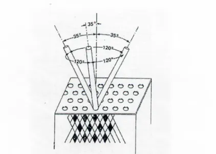
Due to technological difficulties, the fabrication of these crystals were initially restricted to microwave and millimeter-wave frequencies. The early PEG studies concentrated on testing various fee type fabricated c r y s t a l s . E y the introduction of vector wave calculations, scientists proved that the early structures did not have a full band gap due to band crossing along W direction of the Erillouin zone.^^’^® The problem of band crossing was solved by a diamond structure suggested by the Iowa State group of Ho et This predicted structure was later fabricated by drilling a solid dielectric material from three different angles, each 35.26° away from the normal and spread 120° on the a z i m u t h . T h e crystal in the end was a full 3-D fee structure with roughly cylindrical void atoms. This was the first experimental photonic crystal th at possessed 3-D stop band. Along (111) direction, a gap extending from 13 GHz to 16 GHz was observed, with around 50 dE attenuation.
After this verification of the existence of photonic crystals, there was an increased effort in this research area. Scientists searched for new structures th at could be more easily fabricated, and could be scaled down to optical frequencies. A new crystal that meets these requirements was invented by the Iowa State g r o u p . T h e designed
CHAPTER 1. INTRODUCTION
Figure 1.2: The drilling technique used in the construction of the first photonic crystal that possessed 3-D PBG.^^
structure, which was called layer-by-layer photonic crystal, has 3-D PBG, and could also easily be scaled to lower dimensions. Each layer of crystal was formed by dielectric rods arranged parallel to each other separated by a distance a. As seen in figure 1.3, each layer is stacked to the previous one by rotating the layer 90° with respect to the previous layer. Every third layer is parallel to the first one with a shift of a /2 in the direction perpendicular to the rods. The fourth layer is shifted the same way with respect to the second layer. So a unit cell of 4 layers of length c, where every fifth layer repeats the first one, is obtained. The angle between adjacent layers may vary from 90° to 60°. The structure has the symmetry of a face centered tetragonal (fct) type of structure. The crystal can be derived from a diamond structure if 110 chains of atoms were to be replaced by dielectric rods for the special case of c fa —^/2.
This structure is important in the sense that, its dimensions could easily be lowered. Using the anisotropic etching property of Si by KOH, the layers of these crystals were prepared by micromachining techniques at lower scales. First a gap around 100 GHz was reached.^® Then dimensions were further scaled down to achieve a photonic crystal with a full band gap around 500 GHz.^^ By using special silicon thinning methods and double etching the wafers from both faces, this technique could be extended to have photonic
CHAPTER 1. INTRODUCTION
JS X .
3
v L l
= 3 L F = - v U S
Figure 1.3: The design of an fct type of layer-by-layer crystal with a 3-D PEG. The structure is built by an orderly stacking of dielectric rods
30
band gaps around 20 THz.
Using advanced semiconductor processing techniques, this 3-D layer-by-layer structure is recently fabricated at optical frequencies (see Fig. 1.4).®^”^^ With this breakthrough, the application of these crystals at optical frequencies is now feasible.
CHAPTER 1. INTRODUCTION
1.2
Summary of this work
We will first present a dielectric based layer-by-layer photonic crystal. The transmission, reflection and defect characteristics of the crystal will be investigated. A model will be proposed to understand the defect formation. We will then show the enhancement of the EM field within the defect volumes, and suggest a possible application: resonant cavity enhanced detectors built around photonic crystals, where a detector inserted inside the defect volume benefits from the frequency selectivity and the highly enhanced field of the cavity. Next, we will investigate the radiation of the EM fields from a source inserted in the defect volume, and show th at the radiated field has a very high directivity and efficiency.
We will propose waveguides built around photonic crystals. We will show that EM waves could be a guided within a planar waveguide, in which the wave is coupled inside the defect volume, and having no where else to go, propagates through the opening carved through the crystal. The dispersion diagrams for these planar waveguide structures will also be presented, which agrees well with the theoretical expectations. We will also demonstrate the propagation of the EM waves through a single missing rod of the photonic crystal. We will show that the trapped waves may be guided even through a tight corner for these waveguide structures.
We will show that, the metallic structures built in different dimensions and different filling ratios have many superiorities when compared to dielectric-based photonic crystals. A full characterisation of various metallic photonic crystals will be presented, and some possible applications for metallic photonic crystals will be exhibited. A new method to fabricate quasi-metallic photonic crystals using semiconductor micromachining techniques will be demonstrated. The results and advantages of the new structure will be discussed.
Chapter 2
Formation of Photonic Band Gap and
Defects
We constructed a photonic crystal having the geometry of layer-by-layer structure we have described in the previous section. The size of the crystal was chosen to be large for the purpose of easy fabrication, modification and measurement. In this chapter, we will introduce the basic characteristics of the new crystal. First, the band gap will be presented using the transmission and refiection results. Then, the properties of the defects built around this structure will be investigated, and a model to understand the defect formation will be proposed.^®
2.1
Photonic band gap
The layer-by-layer photonic crystal was constructed using alumina rods with a dielectric constant of 3.1 at 12 GHz, with the dimensions 0.32cm x 0.32cm x 15.25cm. In this crystal, we chose a center to center separation of 1.12 cm, corresponding to a filling ratio of ~ 0.29. Figure 2.1 shows the schematics of the measurement set up we used in our experiments.
CHAPTER 2. FORMATION OF PHOTONIC BAND GAP AND DEFECTS
Figure 2.1: Experimental setup for the simultaneous measurement of reflection and transmission from a photonic crystal.
An HP8510C network analyzer and three microwave horn antennas were used to measure both the transmitted and reflected waves. For reflection measurements, we used a metal sheet to calibrate our measurements, where we assumed th at the metal sheet is a 100% reflector at these frequencies. By changing the incidence angle 6, we could obtain the reflection and transmission properties of the photonic crystals at different propagation directions. By using the aforementioned experimental setup, we first investigated the transmission properties of our photonic crystal. The band gap edge values obtained from our transmission measurements along different crystal directions, were very close to the theoretical calculations which predicted a full band gap from 10.6 to 12.7 GHz.^® We then focused our efforts on the reflection measurements.
Although, it was relatively easy to obtain the magnitude of the reflected waves on a reproducible basis, we faced a significant challenge to obtain reproducible phase measurements where we used a metal sheet for calibration purposes. The flatness of the top surface of the photonic crystal and the positioning of the photonic crystal with respect to the calibration metal plate were very critical for a reliable measurement. In our setup, our typical calibration error for the phase measurements was measured to be around q=5°. Figure 2.2 shows the reflection and transmission characteristics of a 16
CHAPTER 2. FORMATION OF PHOTONIC BAND GAP AND DEFECTS 10
Frequency (GHz)
Figure 2.2: Reflection (dotted line) and transmission (solid line) along the stacking direction.
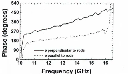
layer crystal along the stacking direction with an incidence angle 5°. The magnitude of the reflected and the transmitted waves were found to be independent of the polarization vector e of the incident EM wave. However, we found a strong polarization dependence for the phase of the reflected waves. Figure 2.3 shows the phase of the reflected waves as a function of frequency for both polarizations where the polarization vector e of the incident EM wave is either perpendicular or parallel to the rods of the top layer of the photonic crystal.
We have discussed the possibility of creating evanescent modes within the photonic band gap by breaking the periodicity of a photonic crystal. Figure 2.4 shows the transmission through a 16 layer crystal with a single missing rod from the 8th layer. A peak in the transmission is observed within the band gap corresponding to a localized mode at a resonant frequency of 12.16 GHz. The quality factor Q factor (quality factor) deflned as the center frequency divided by the peaks full width at half maximum, is 1380, and the peak transmission maximum is 17.7 dB below the incident signal. The polarization vector e of the EM fleld was parallel to the axis of the missing rod. The measurements done for the other polarization showed no resonances.
CHAPTER 2. FORMATION OF PHOTONIC BAND GAP AND DEFECTS 1 1
Frequency (GHz)
Figure 2.3: Experimental reflection phase properties of the photonic crystal for diff'erent polarizations.
Frequency (GHz)
Figure 2.4: Transmission through a 4 unit cell photonic crystal with a single rod missing at the eight layer.
2.2
Fabry-Perot analogy
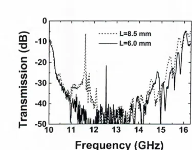
One other way to create defects in this structure is to introduce a planar air gap within the crystal. By separating a 16 layer photonic crystal from the middle with a separation width of L, we built planar defect structures. The transmission through this structures with L = 6 mm (solid line) and L — 8.5 mm (dotted line) are given in figure 2.5. As
CHAPTER 2. FORMATION OF PHOTONIC BAND GAP AND DEFECTS 12
seen from the figure, we can tune the frequency of the defect mode by simply changing the width of the cavity.
“ - 1 0
12 13 14 15 16
Frequency (GHz)
Figure 2.5: Transmission through 4 unit cell photonic crystal with a planar air gap at the middle of width L = 6 mm (solid line) and L = 8.5 mm (dotted line).
Our system can be considered as an analog of a Fabry-Perot resonator, with the introduced planar defect acting as the cavity, and the 8-layer photonic crystals on each side acting as the mirrors.
At this point, we will use the reflection phase information to predict the frequency of the defect modes. The theory we will use is analogous to th at of the Fabry-Perot type of r e s o n a t o r s . I n this analogy, to find the circulating field Ec inside the crystal, we add the transmitted field through the front mirror, and the reflected component after a round trip inside the cavity:^^
Ec = jtxE i (2.1)
where Ei is the initial wave, ii is the transmission coefficient of the front mirror,
and are the reflection coefficients of mirrors, (f>i and <p2 are the reflection-phase factors in radians, /5 is the propagation constant for the travelling EM wave in air, and
L the separation length of the cavity (Fig. 2.6). So, the ratio of the circulating field to
CHAPTER 2. FORMATION OF PHOTONIC BAND GAP AND DEFECTS 1 3
Figure 2.6: The Fabry Perot model
j h
E i 1 —
(2.2)
The resonance condition is satisfied when the phase shift due to one round trip is a multiple of 27t, th at is when 2PL + </>1 + 02 = 2m7r (m = 0, ±1, ± 2 ,...). This resonance condition with the obtained refiection-phase information, can now be used to predict the frequency of the defect mode.
Changing the separation length L of the resonator, we obtained the transmission properties and the frequencies of the defect mode. The defect modes, first appearing at the upper band edge, shifts to the lower band edge of the stop band, as the separation length L is increased. If the separation is further increased to 10.0 mm., we start to observe secondary defects appearing at the upper band edge. In the mean time, the first defect shifts further down to lower frequencies to disappear at the lower band edge. To make a comparison of the theory with the experiment, we added the reflected phase measured from the two walls of the cavity 4>t,ex = 0i + 02· Then, we compared it with the phase that should correspond to the defect frequency in the resonance condition which is given as.
CHAPTER 2. FORMATION OF PHOTONIC BAND GAP AND DEFECTS 14 S e p a ra tio n w id th L (m m ) F req u en cy G H z m- 1 (degrees) m = l F req u en cy (G H z) m=2 M t i ) (d eg rees) m=2 3 13.97 260 4 13.50 230 5 13.13 202 6 12.54 170 7 12.15 156 8 11.78 134 9 11.45 113 10 11.16 92 15.34 352 11 10.86 73 15.01 324 12 10.66 53 14.66 298 13 10.45 34 14.31 274 14 13.98 250
Table 2.1: Experimental measured defect frequencies and corresponding total phase contributions from the walls of the cavity for resonance condition are given for different separation widths, for the first (m = l) and second (m =2) defect modes.
M h ) = "¿m-K - 4ttL ^ (m = 0, ±1, ±2, ± 3 ,...)
c (2.3)
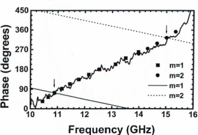
where f i is the measured defect frequency corresponding to the separation width L. Table 2.1 lists the measured frequencies of the defect modes, the value of m and the calculated <f)t{fL) as a function of separation length L. In figure 2.7, the predicted 4>t{fL) and the measured 0t,ex(/) total phase of the two mirrors are compared. As can be seen from the plot, the predicted phase values are in very good agreement with the measured phase values.
Using this reflection-phase information, the frequency of a defect mode for any given separation width L can be found by solving the following equation by an iteration method.
f l = (2m ir - ^i,e i(/z.)l (2.4)
CHAPTER 2. FORMATION OF PHOTONIC BAND GAP AND DEFECTS 15
Frequency (GHz)
Figure 2.7: Comparison of experimental total reflection-phase contribution (thick solid line) of the walls of the cavity, with the calculated values for m = l (squares) and m=2
(circles) for different separation widths. The plot of 0 t(/) for m = l (thin solid line) and m=2 (dotted line) are also shown for L = ll mm.
of the two mirrors (j)t,ex{i) is plotted along with </>*(/) = 2m7r — 47tL^ as a function of / . The defect frequency for the chosen length L can be found from the intersection points of these two plots. As an example, the defect frequency predicted for L = ll mm, is shown in figure 2.7. The plot of 0 t(/) is made for m = l (thin solid line) and m=2 (dotted line), and these two lines intersect with the (j)t,exif) at two frequencies (indicated by arrows in the figure), which are both within the band gap. We see that the agreement between the predicted and experimental defect frequencies is very good. This graphical method also explains the double defect formation for certain cavity lengths. If one of the defect frequencies is closer to the lower band edge, say corresponding to m = l mode, a second frequency satisfying the resonance condition for m=2 can be found. An example where double defects are observed for L=11.5 mm, is given in figure 2.8. The m = l defect mode corresponds to 10.76 GHz, while m=2 mode corresponds to 14.84 GHz. As the separation is further increased, modes corresponding to m=3,4,5,... may also be observed.
Although small in size, there are extra defect modes that does not seem to fit to this theory for any value of m. These extra modes may be due to the oscillatory nature of the <f>t,ex{f), so th at the resonance condition is satisfied at more than one frequency for
CHAPTER 2. FORMATION OF PHOTONIC BAND GAP AND DEFECTS 16
11 12 13 14 15 16 17
Frequency (GHz)
Figure 2.8: An example for double defect formation, where the resonance condition is satisfied for two separate frequencies.
a single mode, say m = l. In other words, graphically, there are more than one point that the expectation line cuts the 4>t,ex{f) for a given m value. Another reason for multimode formation can be the occurrence of secondary resonances, or splittings. This may happen due to the misalignment of the mirrors with respect to each other, and due to the surface roughness of the photonic crystals. These effects may explain the situation, but later experiments done by metallic structures brought some different explanations, which would be discussed in chapter 6.
2.3
Quality Factor
The localization in the cavity obtained in this way can be quite high. The transmission spectra for such a defect where the separation length is 4.6 mm is given in figure 2.9 in an expanded frequency scale. The quality factor of the peak is found to be around 5300, which is the highest value obtained up to now for such a 3-D photonic crystal structure.
A simple approach to relate the quality factors of the defect modes to the reflectivities of the mirrors can be derived by using the Fabry-Perot resonator analogy. If we calculate
CHAPTER 2. FORMATION OF PHOTONIC BAND GAP AND DEFECTS 1 7
Frequency (GHz)
Figure 2.9: Expanded frequency scale for the defect mode, which has a Q factor of 5300.
the square of the field, which is proportional to power:
i E i h ^
Ec ■ (e;)
1 — riV2e~^‘^^
E f t l
(1 — r i r2)^ + 4r i f2 sin “^6
where 6 = ^L -\- (j)t{f)/2. The magnitude of the field drops to its half value at
(1 - T i n f
(2.5)
sin^91/2
4rir2
When the resonance condition is satisfied, 6 will be close to q7r radians, that is 0 ~
qn + 9if2- So full width at half maximum for 6 can be written as
1 - rif2
201/2 — 1/2/2 — (2.6) This is the condition where the peak drops to its half value. The sharpness of the peak is defined with the quality factor (Q) of that peak, which is the ratio of the frequency of the defect to the full width at half maximum:
Q f
CHAPTER 2. FORMATION OF PHOTONIC BAND GAP AND DEFECTS 18
Frequency (GHz)
Figure 2.10: The comparison of inverse of Q values (diamonds) with the corresponding
8 layer transmission (thick solid line).
Assuming linear dependence of (pt{f) on / with a constant a, th at is letting (j)t{f) =
a f within the band gap, we can relate A ^i/2 to A /1/2 as:
-1
/ 2-ïïd o;\ .
-A /i/2 - 1^— + - j A ^i/2 (2.8) and with this formalism, f can be written from the resonance condition as:
f 2 n d
So the quality factor Q value can be calculated from the equation 2.7 as:
m7T
(2.9)
Q
A01h/2 = mTT-1 — y/R\R2 (2.10) where we defined the reflectivities of the mirrors as R\ = r\ and R2 = r^· In our case,
where Ri = R2 = R, and the transmittances Ti = T2 = T = 1 — R are all equal, we may
simplify the Q value to:
^ y/R m-K . . s
Q =
with the assumption that reflectance R is nearly unity inside the stop band. Using this information, a comparison of the Q value, with the transmittance obtained from one wall of the cavity (which is 8 layers), is made. Figure 2.10 shows the transmittance of
CHAPTER 2. FORMATION OF PHOTONIC BAND GAP AND DEFECTS 19
8 layers (solid line), and m-n/Q as a function of frequency of the corresponding defect (diamonds). As can be seen from the graph, the general trend of the plots are similar, however, the experiment does not quite fit to theory quantitatively. The reason may be due to the finite size of the crystal. As we are not using very long rods, the field may not be as localized as the theory presumes, resulting in lower Q factors.
Chapter 3
Resonant Cavity Enhanced Detectors
The fields within the cavities like Fabry-Perot resonators are usually e n h a n c e d . T h i s eflfect has already been used in optoelectronics to achieve novel devices such as resonant cavity enhanced (RCE) photodetectors and light emitting diodes.^® The device within the cavity benefits from the wavelength selectivity and the large increase of the resonant optical field introduced by the cavity. In this chapter, we demonstrate the RCE effect by placing microwave detectors within the localized modes of photonic crystal defect s t r u c t u r e s . T h e experimental results agree well with the predictions of our model.
3.1
Detector inside planar cavity of photonic crystal
A square law microwave detector was placed inside the defect volume of the layer-by-layer dielectric photonic crystal, along with a monopole antenna. The monopole antenna was kept parallel to the polarization vector e of the incident EM wave in all measurements. The dc voltage on the microwave detector was used to measure the power of the EM field within the cavity. We also measured the enhanced field by feeding the output of the monopole antenna into the input port of the network analyzer. The monopole antenna was constructed by removing the shield around one end of a microwave coaxial cable.
CHAPTER 3. RESONANT CAVITY ENHANCED DETECTORS 21
The exposed center conductor which also acted as the receiver, was 2 mm long. The calibrated enhancement measurements were performed in the following manner. We first measured the enhanced EM field by the probe inside the cavity. While keeping the position of the probe fixed, we removed the crystal and repeated the same measurement. This single pass absorption data of the probe was then used for calibration of the first measurement.
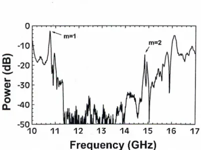
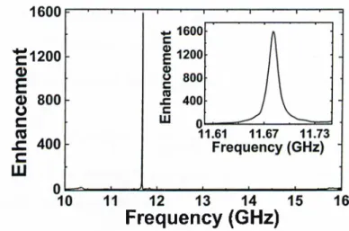
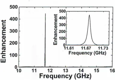
We first investigated the planar defect structure we have described in the previous chapter. Figure 3.1 shows the enhancement characteristics of a planar defect structure with a separation width of 8.5 mm. The measurement was done by the network analyzer and the frequency was chosen to cover the photonic band gap of our crystal. We observed a power enhancement factor of 1600 at a defect frequency of 11.68 GHz. The Q factor was measured to be 900. We then measured the enhancement characteristics of the same defect structure with a microwave detector inserted inside the same cavity (Fig. 3.2). An enhancement factor of 450 along with a Q factor of 1100, were observed at the same defect frequency.
Frequency (GHz)
Figure 3.1: Experimental enhancement factor obtained for planar defect structure using network analyzer.
CHAPTER 3. RESONANT CAVITY ENHANCED DETECTORS 22
Figure 3.2: Experimental enhancement factor obtained for planar defect structure using microwave detector.
3.2
Fabry-Perot model
The discrepancy between two measured enhancement factors can be explained by modeling our structure as a Fabry-Perot cavity.^® The crystals on each side of the cavity are considered as the photonic mirrors of the Fabry-Perot cavity. The probe we used in our experiments was simulated by an absorption region of thickness d, with a relative absorption coefficient a (Fig. 3.3).
The electrical field component for the forward travelling wave E{ can be related to the incident field as:
E f = z---.. . Ei (3.1)
where d is the length of the absorption region. And the backward travelling wave can be related to forward travelling wave as:
(3.2)
Using the equations 3.1 and 3.2, we can write the power enhancement factor rj, which is defined as the ratio of the stored power inside the absorption layer, to the incident EM wave.
CHAPTER 3. RESONANT CAVITY ENHANCED DETECTORS 23
V = {1 + П2е-°‘<^){1-Кг)
1 — 2y/RiR2e~°“^ cos (213L + (j)i3- ^2) + R i R2e~^°“^
where Ri and R2 are the reflectivities of the mirrors of the cavity.
(3.3)
Figure 3.3: Schematics of the Fabry-Perot cavity model with an absorption region of thickness d.
The above result is normalized with respect to the incident field absorbed by the detector in the absence of the crystal. The aforementioned planar defect structure have symmetric mirrors where R = Ri = R2· We used the measured transmission
characteristics to obtain the reflectivities of our photonic mirrors. As the rods are made of high quality alumina with a very low absorption coefficient, the absorption in the crystal can be neglected.^® At the defect frequency, the transmission of an 8-layer crystal was 30 dB below the incident EM wave. The reflectivity of the photonic mirrors was then obtained as R = 1-T = 0.999. The ideal case which maximizes 77 corresponds to
ad = 0, which gives a maximum enhancement factor of 2000. We then varied ad to
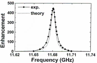
obtain enhancement factors closer to our experimental measurements. For ad = 0.0001, Eq. 3.3 yields an enhancement factor of 1600 (which corresponds to the value obtained from the network analyzer), while ad = 0.0011 results in an enhancement factor of 450 (microwave detector). The increased absorption factor for the detector measurement can be explained by the relatively large volume size of the microwave detector compared to monopole antenna alone. Figure 3.4 compares the measured (solid line) and simulated (dotted line) enhancements obtained for the RCE microwave detector within the planar
CHAPTER 3. RESONANT CAVITY ENHANCED DETECTORS 24
defect structure. The theoretical Q-factor (1500) is comparable with the experimental Q-factor (1100).
Frequency (GHz)
Figure 3.4: Comparison of the experimental (solid line) and theoretical (dotted line) enhancement factors for the detector inside planar cavity.
3.3
Tuning bandwidth
Fabry-Perot model suggests th at rj is maximized for the matching case Ri —
To increase the enhancement, we increased R2 by adding one more unit cell (4 layers) to the mirror at the back. This resulted in an asymmetric planar cavity with a 2 unit cell thick front mirror, and a 3 unit cell thick back mirror. By varying the width of the planar cavity, we measured the enhancement factors at different resonant frequencies. As shown in Fig. 3.5, the tuning bandwidth of the RCE detector extends from 10.5 GHz to 12.8 GHz. This tuning bandwidth of the RCE detector is in good agreement with the full photonic band gap (10.6-12.7 GHz) of the crystal.^® As expected, the measured enhancement factors are relatively higher when compared with the symmetrical defect case. The maximum enhancement was measured to be 3450 at a defect frequency of 11.75 GHz. The theory predicted enhancement factors around 5500, which is higher than the measured values. The discrepancy can be explained by the finite size of the
CHAPTER 3. RESONANT CAVITY ENHANCED DETECTORS 25
photonic crystal, which limits the power enhancement of the field within the cavity.
Frequency (GHz)
Figure 3.5: The power enhancement can be obtained at different frequencies within the band gap by changing the width of the cavity.
3.4
Box-like cavity
In order to obtain a defect that is localized in three dimensions, we modified a 16 layer crystal structure in the following manner. Part of the rods on the 8**^ and 9*^ layers were removed to obtain a rectangular prism-like cavity. The dimensions of the cavity was 4a x 4a X 2d, where a = 1.12 cm was the center to center distance between parallel rods, and
d = 0.32 cm was the thickness of the alumina rods. We measured the power enhancement
characteristics of this structure using the method described earlier. Figure 3.6 (dotted line) shows the measurement made by the network analyzer. An enhancement factor of 290, and a Q factor of 540 were measured at a defect frequency of 12.32 GHz. We then used a microwave detector within the cavity to probe the EM field inside the localized defect. As shown in Figure 3.6 (solid line), the maximum enhancement (245) occurred at the same frequency, along with a Q factor of 680. Both measurements clearly indicate the resonant cavity enhancement for the localized defect.
CHAPTER 3. RESONANT CAVITY ENHANCED DETECTORS 26
Although the one dimensional Fabry-Perot cavity model will be a crude approxima tion for such three dimensional structures, the reduced power enhancement (along the stacking direction) can still be explained by this simple model. The photonic mirrors of the box-like defect structure were made of 7-layers (instead of 8). In contrast to the planar defect structure, these photonic mirrors were not symmetric. For the first mirror.
Frequency (GHz)
Figure 3.6: Enhancement characteristics of the box like cavity.
the polarization vector e was perpendicular to the rods of the first and seventh layers. On the other hand, the polarization vector e was parallel to the first and seventh layers of the second mirror. This brought an asymmetry to the reflectivities of each mirror, where we measured Ri = 0.978 and R2 = 0.998 for propagation along the stacking direction. Using these reflectivity values in Eq. 3.3, we calculated an enhancement factor of 300 for the measurement made by the network analyzer (with ad = 0.0001), and 250 for the microwave detector (with ad = 0.0011). Both of these predicted values agree well with the experiment.
Chapter 4
Highly Directional Resonant Antennas
Among the most important applications of photonic crystals, there is a great deal of growing interest for photonic crystal-based a n t e n n a s . I n microwave and millimeter- wave integrated circuits, the control of the radiation from a dipole antenna is of great importance. In such circuits, the antenna is mounted on a semiconductor substrate, which enhances the performance and functionality of the circuit. But most of the power from the antenna on a dielectric substrate is radiated into the substrate. Standard antennas on GaAs or Si radiate only 2-3% of their power into air. If a thin substrate is used to overcome the loss due to this trapping, another problem arises. A 180° phase shift comes from the reflection at the bottom conductor, resulting the radiation to cancel out at driving point. These problems can be solved, if the antenna was to be mounted on a 3-D photonic crystal, from which the radiation will fully be reflected in all directions.
The reported experimental and theoretical studies on the antenna applications mostly made use of the total reflection property of photonic crystals. The antennas mounted on photonic crystal substrate surfaces exhibited high efficiency and directivity compared to conventional antennas on dielectric substrates. Although high directivities which could be achieved using array antennas on photonic crystals were suggested,'*^ the maximum directivity that was demonstrated by Brown and McMahon using a photonic crystal-based single dipole antenna was 10, along with a radiative gain of 8.^° Very
CHAPTER 4. HIGHLY DIRECTIONAL RESONANT ANTENNAS 28
recently, a higher gain around 80 was reported using a 2-D photonic crystal cavity and a metallic mirror.
In this chapter, we report a photonic crystal-based resonant antenna with a very high directivity and gain. The antenna was formed by a hybrid combination of a monopole radiation source and a cavity built around layer-by-layer photonic crystal.
4.1
Radiation patterns
We used the output port of a microwave network analyzer and a monopole antenna to obtain EM waves. The monopole antenna was constructed by removing the shield around one end of a microwave coaxial cable. The cleaved center conductor, which also acted as the radiation source, was 6 mm long. The chosen length of the monopole antenna corresponds to a quarter wavelength of EM wave at a frequency of 12.5 GHz, which is close to the adjusted resonance frequency of the cavity. Input port of the network analyzer and a standard gain horn antenna were used to receive the radiated EM field from the monopole antenna. The receiver was kept free to rotate around the antenna as shown in Fig. 4.1.
We investigated the radiation characteristics of this monopole antenna, which was inserted into the planar defect structures built around a photonic crystal that consisted of 20 layers. The planar defect was formed by separating the 8*** and layers of the structure. In order to suppress the radiation in the backward direction, we intentionally chose one of the crystals of the cavity to have a higher refiectivity than the front crystal. This resulted in an asymmetric planar cavity with a two unit cell (8 layers) front crystal, and a three unit cell (12 layers) back crystal. The intensity through the back crystal is ~ 18-20 dB lower than the front crystal in the 0° direction. If a symmetric cavity was used, two directional beams would emerge in both directions.
In the H-plane measurements, the antenna and the polarization axis of the receiver horn antenna was kept vertical, and were parallel to each other at all incidence angles.
CHAPTER 4. HIGHLY DIRECTIONAL RESONANT ANTENNAS 29
Figure 4.1: Experimental setup for measuring the radiation patterns of the monopole antenna at various angles.
We then rotated the antenna, photonic crystals and the horn antenna 90 degrees (so that the monopole antenna and the polarization axis of the horn were horizontal) to measure the radiation pattern in the perpendicular plane (E-plane). In all these measurements, the monopole antenna was kept close to the back crystal of the cavity. The antenna was parallel to the surface rods of the back crystal to maximize the directivity and the detected power.
Antenna radiation patterns were simulated by R. Biswas of ISU, with the widely used finite-difference-time-domain (FDTD) technique.^® To reduce the FDTD computational space, a short dipole antenna was used in the simulations which should approximate well the monopole antenna. The time dependent Maxwell’s equations were numerically integrated with the fixed frequency dipole source inside the defect volume of the photonic crystal, to obtain the far-field radiation pattern. The calculations were repeated at different frequencies of the dipole source.
We first measured the detected power at the resonance frequency of the cavity as a function of angle. Figure 4.2(a) (solid line) shows the normalized radiation pattern in H-plane, which was measured at the resonance frequency of the cavity. We observed a
CHAPTER 4. HIGHLY DIRECTIONAL RESONANT ANTENNAS 30
Figure 4.2; The measured (solid lines) and calculated (dotted lines) radiation patterns of the monopole antenna inside the cavity of the photonic crystal for (a) H-field and (b) E-field. The measurements and simulations were made at the resonance frequency of 11.7 GHz.
strong radiation around 0 = 0°, where the radiation along other directions is highly suppressed. The measurements performed in the other plane (E-plane, Fig. 4.2(b), solid line) also resulted in a similar radiation pattern. The measured (solid lines) and calculated (dotted lines) radiation patterns for both planes agree well. The simulations also predict a directed radiation pattern that displays the same trends but has side lobes
CHAPTER 4. HIGHLY DIRECTIONAL RESONANT ANTENNAS 31
other than the major lobe. We also observed such radiations along similar angles in the experiment, but we were able to suppress them by slightly varying the position of the monopole antenna within the cavity. We repeated these measurements with antennas having different lengths, and we observed no significant change in the radiation patterns for both planes.
4.2
Characterization
For antennas with one narrow major lobe and negligible minor lobes in the radiation pattern, the maximum directivity is approximately equal to^^
47T " e ; e ; ·
where ©i is the half-power beamwidth in one plane and 02 in the perpendicular plane to the first, in radians. The measured half-power beamwidth along the H-plane (Fig. 4.2(a)) was 12 degrees, and was 11 degrees along the E-plane (Fig. 4.2(b)). These values lead to a directivity value around 310.
Figure 4.3(a) (solid line) shows the detected power as a function of frequency at
0 = 0°. The dotted line displays the detected power at the same angle in the absence of
the photonic crystal. At resonance frequency, we observed a power enhancement factor of 180 (22.6 dB) at a defect frequency of 11.725 GHz. The radiated EM field from the monopole antenna has also frequency selectivity introduced by the cavity. The Q factor was measured to be 895.
In order to understand the effect of the resonator to the efficiency of the monopole antenna, we also measured the S-parameters of our antenna structure. Figure 4.3(b) shows the reflection power coefficient (S ll) which is 30% (-5 dB) for the monopole antenna standing alone in air. This implies that the antenna radiates only 70% of the incoming power. When the antenna was inserted inside the cavity, we observed a very sharp drop (-35 dB) at resonance frequency in the reflection spectra [Fig.4.3(b), solid
CHAPTER 4. HIGHLY DIRECTIONAL RESONANT ANTENNAS 32
line]. This drop indicates th at most of the power (99.97%) is radiated out in the presence of the cavity. The maximum radiation gain for our antenna is related to the maximum directivity by Go = (1 — R){1 — A )Dq, where R is the reflected power and A is the
absorptivity of the antenna. In our case, the reflectivity at the resonance frequency is very small (0.0003). Assuming that the absorption in the antenna has a negligible value, the maximum gain has a value 300.
Such a planar cavity built around a 3-D photonic crystal should not be confused with the Fabry-Perot type of resonators th at are constructed by using distributed Bragg reflectors (which are known as 1-D photonic crystals). In the former structure, the EM field is always coupled to the evanescent defect mode within the band gap irrespective of the incidence angle. However, the resonant frequency shifts as the angle of incidence of the EM wave changes in the latter case.'^^·'*'^ It is obvious that for planar waves, 3-D and 1-D resonant structures will result in similar enhancements and directivities. In our case, the monopole antenna radiates in all directions, and all the power radiated is coupled to the evanescent mode of the defect, regardless of the direction. This is the reason we have an antenna with a very high efficiency [see Fig.4.3(b)j. However, for a 1-D structure, the radiated EM field, except a certain direction, will not be coupled to the corresponding resonant mode of the cavity.
Although our structure is suitable for narrow bandwidth applications, one can tune the defect frequency to any desired value by adjusting the width of the cavity. We observed that the resonance frequency could be tuned within a frequency range extending from 10.6 to 12.8 GHz, which corresponds to the full band gap of our photonic crystal. The directivity drops to values around 100 at the band edges, and reaches a peak value of 310 at 11.7 GHz.
CHAPTER 4. HIGHLY DIRECTIONAL RESONANT ANTENNAS 33
Frequency (GHz)
Figure 4.3: (a) Detected power of the monopole antenna with (solid line) and without (dashed line) photonic crystal around resonance frequency at ^ = 0°. (b) The reflection power coefficient (S ll) measured with (solid line) and without (dashed line) photonic crystal.