N O \ / E i . MM * 4 Siipi^ ^ ^ '*»w . v-i i :?i< ^ , .:; ·' ^. ;> * '\i^. i '..^ ^ ‘C’ , m*“.·,■ W i - U. i . 3 ; -U B M IT T E D 7C ' T H F D E P A R T M 'S N T C r cL.· E L S C T fi:0 'N IC S Ef^iiS'"^45EP.r.7 ¿ .n D T H E IN S T IT U T E : O F ENGor-rEF=Kj\:B; A 0 ? B JLKEHT U : ^ iv £ P 0 F 7 .' m ?ARTi.^L FU- ?; ;„U' /5 -;T
iV:.r-..::^'; <*^•»4 4Nk· « «i ^ t «· < f ’< ^ k£« 1.*^' <·, *' ·'■. ·· * · « <«r · , h ^ ‘ ( *■-T K ■ i;»· 7 8 8 ^ - 6 y ~
'K SS
1331
NOVEL FILTERS FOR SIGMA-DELTA A /D
CONVERSION
A THESIS
SUBMITTED TO THE DEPARTMENT OF ELECTRICAL AND
ELECTRONICS ENGINEERING
AND THE INSTITUTE OF ENGINEERING AND SCIENCES
OF BILKENT UNIVERSITY
IN PARTIAL FULFILLMENT "-F THE REQUIREMENTS
FOR THE DEGREE OF MASTER OF SCIENCE
Bv
A. Ertugrul KOLAGASIOGLU
April 1992
'f 8 S \ 6 i d d i
I cei'tiiy that I havei'ead this tliesis and that in rny opinion it is fully adequate, in scope and in quality, as a thesis for the degree of Master of Science.
Assist. Prof. Dr. Mehmet .Ali Tan(Principal Advisor)
I certify that I liave read thi.s iliesis and tluit in my opinion it is fully adequate, in scope and in quality, as a. thesis for the degree of .Afiistei' of Science.
Abdullah Atalar
I certify that I have read this ifiesis and that in my opinion it is fully adequate, in scope and in quality, as a thesis for the degree of .Master of Science.
Assoc. Prof. Dr. Ellis Çetin
Approved for the Institute of Engineering and Sciences:
P
________________________Prof. Dr. Mehmet Bara}'
ACKNOWLEDGMENT
I would like to thauk Assist. Prof. Di·. Meliiuet Ali d'an for hi.s supervision, guidance, suggestions and encouragement throughout the development of this thesis.
It is a pleasure to express my thanks to all my friends for their valuable discussions and to my family for providing morale suj^port throughout this study.
ABSTRACT
NOVEL FILTERS FOR SIGMA-DELTA A/D CONVERSION
A. Ertiigrul KOLAGASIOGLU
M.S. ill Electrical and Electronics Engineering
Supervisor: Assist. Prof. Dr. Vlehrnet Ali Tan
April 1992
Oversampled data conversion teclmiques based on sigma-delta modulation lias an increa.sing popularity. The main reason beliind this fact is the recent developments in VL.SI technologies especially in CMO.S VLSI. These kind of converters have several ad\'antages such as robustness, no trimming, no error correction, good noise performcince. etc. This thesis presents .several kinds of high resolution converter structures. It states advantages of second order sigma-delta conversion teclinique. hollowing this discussion, a new imiilemen- tation of the second order sigma-delta modulation with a single feedback loop is introduced which can be imiilemented in a smaller area.. The performance, of the system is estimated with some digital decimation filters, one of whicli is an extended version of standard .smA filter that can be integrated in a chip with a small die size.
Keywords : Oversampling, VLSI. CMOS, sigma-delta modulation.
ÖZET
SİGMA-DELTA A/D ÇEVİRİCİLER İÇİN YENİ FİLTRELER
A. Ertuğrııl KOLAĞASIOĞLU
Elektrik ve Elektronik Mühendisliği Bölümü Yüksek Lisans
Tez Yöneticisi: Doç. Dr. Mehmet Ali Tan
Nisan 1992
Sigma-delta aşın örnekleme, tekniklei’i günümüzde önemim .sürekli arttır maktadır. Bunun esas sebebi büyük l)ir hızla geli.şen VLSI özellikle CMOS VLSI teknolojisidir. Signicudelta çeviricilerinin bir çok avantajları arasında, de vredeki idealden sapmalara karşı az duyarlı olması, üretim için pahalı teknolo jiler gerektirmemesi, hata düzeltme devrelerine ihtiyaç duymaması ve bu çeviri cilerde gürültünün çok az olması sayılabilir. Bu çalı.şma, çe.şitli yüksek çözümle- meli çeviricileri inceler ve bunların a.ra.smda ikinci dereceden sigma-delta çevi ricilerinin üstünlükleri üzerinde durur. Daha sonra ikinci dereceden sigma- delta çeviricilerinin yeni bir uygulaması olarak daha küçük ¿dan kaplayan tek geri beslemeli ya.])inm olıuşturulmasmı ve bu yapının ç.e.şitli sa.yısal filtreler ile elde edilen sonuçlarını gösterir. Bunların arasında geliştirilmiş sinc^ filtre en tegre devre içinde yerleştirme kolaylığı açısından da önemlidir.
Anahtar kelimeler : a.şırı örnekleme, VLSI, CMOS, sigma-delta çevirici.
C o n ten ts
1 IN TR O D U C TIO N 1
2 ON A /D CONVERTERS 3
2.1 Basic Convertoir .Structures... 3
2.1.1 Flash C o n v e rte rs... 3
2.1.2 Successive Approximation C o n v erters... 3
2.1.3 Chcirge Redistriliution C o n v erters... 5
2.2 Design C r i t e r i a ... 6
3 SIGMA-DELTA CONVERTERS 9 3.1 First and Second Order Sigma-Delta C o n v e rte rs... 11
3.1.1 Performance analysis on linearized m o d e l... 15
3.2 Other Sigma-Delta C onverters... 18
4 NOVEL STRUCTURES AND SIMULATIONS 20 4.1 Novel Loop F i l t e r ... 20
4.2 Novel Implementation of Decimation F 'ilter... 22
4.3 Limits and Com parison... 29
4.4 Expected size and c o m p le x ity ... 32
CONTENTS Vll
5 CONCLUSION
5.1 Future Work
34
35
List o f F igu res
2.1 Ba,sic structure of 2-bit fla.sh c o n v e r te r ... 4
2.2 Basic structure of n-bit successive approximation converter . . -5
2.3 Basic. Structure of 3-bit Cliarge Redistribution Converter . . . . 6
2.4 Characterization of Errors in A/D C o n v e rte rs ... 8
3.1 Basic sigma-delta modulator s t r u c t u r e ... 11
3.2 illustration of low-pass filtering ... 12
3.3 First order modulator output ... 13
3.4 Second ordei· modulator o u t p u t ... 14
3.5 Digital decimation filter ... 14
3.6 Double loop sigma-delta modulator structure ... 15
3.7 Modelling the ciuantizer as the noise source ... 16
3.8 Noise shaping curves of sigma-delta m o d u la to rs ... 18
4.1 Timing phcises for the implementation of H ( z ) ... 22
4.2 Simplified current mode implementation of H ( z ) ... 23
4.3 Block Diagram of the digital decimation f i l t e r ... 26
4.4 Magnitude characteristic of sinc^ f i l t e r ... 27
4.5 Magnitude characteristic of sinc^ filter around signal band . . . 28
LIST OF FIGURES IX
4.6 Output spectrum of the m o d u la t o r ... 30
C h ap ter 1
IN T R O D U C T IO N
Forty year old principle of .sigjiia-delta modulation is getting more and more popular nowadays [l] [2]. The main reason behind· this is the tremendous improvements in VLSI, especially in CMOS VLSI teclmologies. However, as it is usually the case, improvements in ojie measure usually results degradation in another one. Low jiarasitic ca|)acitances and small feature size of new VLSI technologies allow opei’ation at very high clock I’ates, whereas poor component matching and reduced sup])ly levels degi'ades the performance of analog circuits more and more [3].
On the other end, there is a growing tendency for implementation in digital domain. The excellent noise performance and easy jiixjgramming features of digital circuits allow them to dominate analog circuits in most of the applica tions. However, analog circuits are still ( and will alwa3^s be ) necessary, at least for interfacing because everything in the world is analog. This growing interest on digital systems gives rise to the demand for higher performance data converters. There are basically two constraints; the speed and the resolution. For the converters which require both high speed and high resolution, there is no other way but using expensive technologies. High speed medium resolution converters can be fabricated quite easily within the limits of the technology.
Finally, when medium speed very high resolution converters are required, sigma-delta oversanqiling systems offer a very attractive solution. For very high resolution analog to digital and digital to analog conventional data converters either require laser trimming or error correction algorithms [4] [5]. On the other hand tlie sigma-delta converters have the great advantage as to exchange the resolution in time for that in amplitude [6].
CHAPTER 1. INTRODUCTION
of all, a very course RC filter is sufficient as an anti-aliasing filter because of having extremely high oversampling rates. Furthermore, the system can be integrated within a very small chip area using inexpensive technologies. .Since most of the chip area is consumed by the digital decimation filter, the system is well suited to the scaling of technologies. Because of these and many other reasons, the future will make sigma-delta converters the only choice whenever the speed requirement can lie met.
The major difference between sigma-delta converter structures is the order of integration which will be explained in chapter 3. .A.s the order of integra tion increases, noise shaping of the system performs better, leading to higher resolutions. What makes the sigma-delta converters most attractive among different types of converters is its robustness. The first order system is the best Irorn that point of view but, uiu'ortuuately to ha\e a resolution of 16 bits, an oversampling ratio of 2400 is required [3] whicli is not feasible. The second order converter structure shows a similar robustness and it can reach very high resolutions quite easily. Higher order modulation schemes always suffer either from the stability or from mismatch problems [7] [8] [9]. Therefore, the sec ond order converter structure is generally employed to obtain high resolution
sigma- converters.
This thesis proposes a new single loop second order sigma-delta converter structure and provides a comparison between conventional data converters and the newly proposed one. VVith this motivation, the second chapter briefly ex plains basic converter types and the characterization of converters. Then, the third chapter introduces the sigma-delta modulation. The general advantages of the sigma-delta technique is investigated and the theoretical performance es timation is discussed. In the forth chapter, the new structure which shows the same ¡performance with the standard second order system is proposed. The oretical and simulated results for the new structure is presented. The results are compared with the previously reported values. Finally, the improvements, aj)plication areas and future work are stated in cliapter 5.
C hapter 2
O N A /D C O N V E R T E R S
2.1
B asic C on verter S tru ctu res
Id this section basic con\’erter structures will be introduced and some of the advanta.ge.s of the structui'es are discussed for furthei- comparison with sigma- delta data cont erters.
2.1.1
F lash C on verters
The flas h conversion, is the most obvious way of analog to digital conversion [10]. In flash conversion, if n bit of resolution is retjuired the input voltage is compared with 2“ — 1 reference voltages and a thermometer type output is obtained. This output is then encoded to binary representation. This type of conversion can be completed in one clock cycle, therefore it is extremely fast. However, it requires 2’“ — 1 comparatoi's and an encoding logic. Because of the intolerable area consumption, it is not used for high resolution converters unless the speed requirement is crucial. Basic structure of 2-bit flash A/D converter is shown in Fig. 2.1.
2.1.2
S u ccessiv e A p p ro x im a tio n C onverters
The successive approximation method requires just a single comparator and a feedback n-bit digital to analog converter [10]. First, the most significant bit to the digital to analog converter is set to 1 and the output of it is compared with the analog input. If the analog input is smaller, then the most significant bit
CHAPTER 2. ON A/D CONVERTERS
rci'
D 0
D
CHAPTER 2. ON A/D CONVERTERS
V
Figure 2.2: Basic structui'e of n-bit succe.ssive approximation converter
i.s reset to zero otherwise it remains 1 until the end of the conversion. Then, the same procedure is applied to the other bits towards the least significant one successively. After the last decision, the output word is the valid digital representation. In that way the com'ersion is completed in n cycles. The |.)erformance of tliese type of converters depends on the ])erformance of the digital to analog converter. Iherefore. higii resolutions are hard to achieve. The Irasic structui'e of a.n n-l.)it successive ajrproximation converter is shown in Fig. 2.2.
2.1.3
C harge R e d istr ib u tio n C onverters
Charge redistribution converters are commonly used when high resolution and medium speed conversion is required [11]. The idea is an indirect approach. Since the capacitor matching in CMO.S technology is quite good, one can im- ])lement the successive iipproximation in charge domain. The adv¿uitage of this
CHAPTER 2. ON A/D CONVERTERS
Figure 2.3: Ba.sic Structure of 3-bit Charge Redistribution Converter
a])])roa.ch is that it does not require digital to analog converter. The perfor mance of the converter is limited by the capacitor matching. Ex'pensive MOS technologies, e.g. one using laser trimming, can achieve very high resolutions. Furthermore capacitance spi'ead is quite large which results a relatively large area requirement. The basic structure of a 3-bit cluirge redistribution converter is given in Fig.2.3.
2.2
D esig n C riteria
In ordei· to ca.tegoi'ize analog to digital converters there exist man}' criteria, one ai^plication may require one of them to be the best while it has no importance for another one. VVe can outline some of them as follows.
Oversampling
Usually signals are sampled at frequencies which are higher then the Nyquist rate. The main reason for this is the filtering requirements and limitations for
CHAPTER 2. ON A/D CONVERTERS
the following sections of the circuit. The ratio of sampling frequency to the Nyquist frequency is called the over sampling ratio.
O S R = ^
JN (2.1)
Resolution
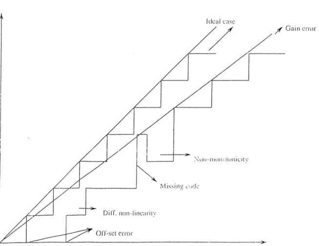
The resolution is usually one of the most imjrortant j^arameters of a data converter. It is S])ecified as the numlrer of bits. Having a resolution of n-bits means that the error in the output woi’d is less than K .,//(2“)
Gain Error
In an ideal converter the average slope of the transfer characteristics is unit}·. Any deviation from unity is called the gain error in actual converters. Gain erroi· reduces the dynamic range of the converter. However, it can be compensated by other means.
O f f s e t Error
The real transfer characteristics of a. converter does not start at where it should. In other words the input level that 00..00 to 00..01 transition should occur is shifted. This is called the offset error. Offset error onl}' affects the DC value in output spectrum.
Missing Codes
In certain cases, one output word may never occur because of non ideal effects in components of the converter. 'This output word is called the missing code. It has detrimental effects on output spectrum.
D i f fe re n ti a l N onlinearity
The differential nonlinearity is the deviation fi'om tlie ideal spacing of the transition voltages in an analog to digital converter [12]. As the error, abso lute maximum value is specified. The differential nonlinearity exists in every converter but it should be smaller than the half of the least significant bit.
Integral N onlinearity
The integral nonlinearity specifies the overall shape of the analog to digital converter characteristic [12]. It is the measure of the maximum deviation of the
CHAPTER 2. ON A/D CONVERTERS
Figure 2.4: Char?'''t'erization of Errors iu A/D Converters
actual transition points from the straight line drawn between the end points.
Non — monotonicity
If any wheie in the transier characteristic a negative sloj)e occurs, the con verter is non-monotonic. Non-monotonicity is usually intolerable. It has serious effects in output s]>ectnim. Tlierefoi(i, error correction techniques are used to overcome this problem.
In order to ex])lain all tliese non ideal effects Fig.2.4 is constructed. Al though such a converter lias no commercial value, it is a.n interesting case to study.
C h apter 3
SIG M A -D E L T A C O N V E R T E R S
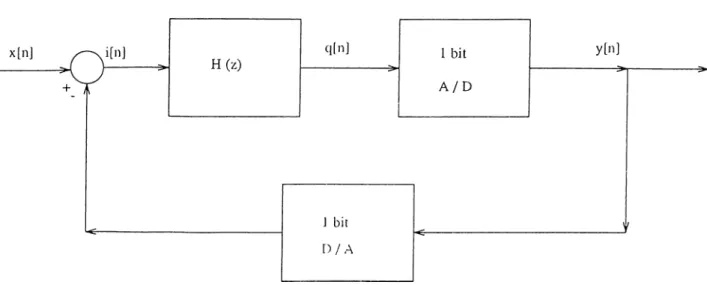
1 he main idea of sigma-deltii com'ersion is Lo excliange resolution in time to that in amplitude [6]. To achieve this goal, a two-level quantizer and a two- level digital to analog converter is used. Having a two-level digital to analog converter in the feedback loop means that you either switch to or Vcc- In that way, always the exact conversion is achieved. This perfect feedback loop ])rovides very high robustness to the system against the comi^onent mismatches. Then, a very high oversampling rate together with a noise shaping function is used to obtain desired resolution at Ny'quist rate.
The most attractive feature of sigrna-delta conversion is that it is quite easy to achieve high resolutions with inexpensive technologies. Whenever the speed requirement can be met, these types of converters will override others because they are cheaper and the}· will be much more cheaper in near future.
Some of the advantages of the sigma-delta converters can Ire stated as fol lows
• An anti-aliasing filter is required at the input but it can be implemented b\· a single RC network because the required stop band of the filter and the required pass band of the filter are far apart from each other due to high oxersampling rates.
• Due to very high over sampling rates tlie input is almost constant within one sampling period. That is to say, no sample cuid hold circuitry is required which is one of the most importcint problems in other kinds of converters. •
• High resolutions can be achieved without excessive chip area and without expensive technologies.
CHAPTER 3. SIGMA-DELTA CONVERTERS 10
• Most of the chip is used by the digital decimation filter therefore the system is well suited to scaling of the ])rocess. Whereas, the standard con verters are mostly composed of analog elements so scaling bring almost no improvement for them after a certain limit.
• The one-bit digital to analog feedback loop gives high robustness to the system which requires only error tolerable component matching. Consequently, no laser trimming, chopping stabilizers, offset nulling, error correction tech niques are required.
• Due to very small number of analog components, the internal noise per formance is excellent.
• Both the internally generated noise and the input noise is shaped by the modulator and than filtered by the digital low pass hlter. Hence most of the noise is eliminated. If the inj^ut is noisy, the output SNR is better than the output SNR of any other conversion scheme.
• If the converter structure is dt^signed accordingl}', the user can easily choose his application-specific speed and resolution, definitely this should be within the limits of the device. The extra hcirdwcire required for such an im plementation is almost negligible.
Since the sampling rate of sigma-delta convertei's are limited to a base band of iOOKHz, cireas of application are also limited. .A.s examples, voice band coders, audio band coders for compact-disk recorders, digital audio tapes, mini disc, ISDN applications, and high performance single-chip signal processors are major topics of interest.
Inherently, there are two problems of sigma-delta converters. First of all they are rather slow due to large oversampling rates. ,Secondly,it is very hard to simulate them in circuit level due to time, memory and resolution problems. For instance, a high resolution simulation of a switched analog circuit requires at least 100 point trcinsient analysis to be Ccilculated in each clock. If we want to have an 1024 point FFT with an oversampling ratio of 256 then
1024 * 100 * 256 = 26214400 (3.1)
points should be calculated in transient analyses. Furthermore, this calcula tions should be done with a precision greater than the resolution of the con verter. All of these, make the computer-aided behavioral level simulations essential. These behavioriil simulations has to be done in such away that one
CHAPTER 3. SIGMA-DELTA CONVERTERS 11
Figure 3.1: Basic .sigma-delta modula.tor .structure
should be able to distinguish whether the .system is stable, robust, possible to implement etc.
3.1
First and Second Order S ig m a -D e lta C onverters
Basic structure of a sigma-delta modulator is shown in F'ig.3.1. This struc ture can be analyzed both as synchionous and asynchronous. However, for implementation purposes, we will deal with the synchronous system and con- secpiently signal in every level will be considered in discrete time.
In this structure H{z) stands for the loop filter which pushois the noise out of the signal band. The Cjuantizer is a one-bit analog-to-digilal converter and just distinguishes weather q[n] is greater or smaller than the reference value. The one bit digital to analog converter also has perfect linearity due to its two-point output. The operation oi the block diagram is straight forward.
What converts a sigma-delta moduhttor to a sigma-delta data converter is the digital decimation filter. The decimation filter in Fig.3..5 takes the modu lated spectrum Y{z), low pass filters the shaped noise to get the desired signal and decimates to a desired sampling rate around the Nyquist rate. So, from the users point of view, it is just a standard data converter. One important prop erty of that digital decimation filter is that it does not require any multipliers
CHAPTER 3. SIGMA-DELTA CONVERTERS 12
m-bits FIR filter coefficients
Figure 3.2: An illustration of low-pass filtering
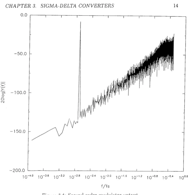
because the input is just 1-bit. An other interesting point may be having high resolutions at the output while the input is is just a 1-bit stream, however, as can be seen from Fig. 3.3 and Fig. 3.4 1-bit input stnoam Y(z) carries enough information for the high resolution output if the out of band quantization noise is removed. Output spectrums of first and second order modulators are given in Fig. 3.3 and Fig. 3.4 respectively. Notice that / / / . s axis is also in log scale to have readable plots. .An illustration of low-pass filtering is given in Fig. 3.2, also a more detailed HR implementation is can be found in Fig. 4.3.
Recently, the double loop modulators overi'ide the early popularity of the single loop systems. Since the noise in the. single loop modulators highly cor related with the input, high resolutions are infeasible to reach [3] [13] [14]. For example, an oversampling ratio of 2400 is required for a single loop system to achieve the resolution of 16 bits. Therefore, the need for faster and higher res olution converters result in higher order modulation techniques. Among these higher resolution converters second order one is the most attractive because of the inherent stability problem in higher order systems.
Both stability and robustness of the second order system makes it an appro priate choice for medium speed high resolution converters. Since the output noise is almost uncorrelated with the input [6], even resolutions which are higher than 14 bits are attainable. However, for such resolutions the internally generated noise becomes as important as the quantization noise.
CHAPTER 3. SIGMA-DELTA CONVERTERS 13 CT' O O CN - 120.0
CHAPTER 3. SIGA4A-DELTA CONVERTERS 0.0 14 1 I I---1---r 50.0 -CTI
o
o C\l •100.0 -150.0 -200.0 J ________ L J ________ I________ I________ !________ L 10“ ^ · ° 10" ^ · ® 1 0" ^ · ^ 10’ ^ '® 1 0“ ^ · '' 10“ ^ · ° 1 0“ '· ® 10· ' · ^ 1 0‘ ° · ® 10“ ° · ' ' 10° · ° f/fsFigure 3.4: Second order modulator output
CHAPTER 3. SIGMA-DELTA CONVERTERS 15
Figure 3.6: Doul)le loop .sigma-delta modulator structure
For resolutions below 10 bits, production cost of iii'st order converters is lower than that of the second ordei' ones. However, for higher resolutions, the length of digital decimation filtei' increased drasticall}' for the first order sj'stems, consequenth· second order s3'stems become much more cost effective.
3.1.1
P erform ance an alysis on linearized m od el
The i)erformance of sigrna-delta converters basically de])ends on the noise shap ing characteristics of the modulator. The inherent noise source in the system is the one bit quantizer. It is given, in for example [1], that for any linear q step quantizer, the power of the noise source is uniformly distributed in the band [0,/s] with the spectral density
Eif) =
F2./; (3.2)
However, only this spectral density gives no information to us because the effects of loop filter are still unknown. .Since the system is inherently non-linear ( because of analog to digital and digital to analog converters ) no exact calcu lations can be performed on theoretical basis. So either asymptotic evtiluations [15] [13] [14] are carried out or the system is linearized by replacing the quan tizer with an additive noi.se source [1]. Here we will deal with the linearized model, because it is easy to understand and the results of both analysis agree
CHAPTER 3. SIGMA-DELTA CONVERTERS 16
w[n]
f'igure 3.7: Modelling the quantizer as the noi.se source
with each other. The modelling of the one-bit quantize)· with an additive noise source gives ns the structure in Fig.3.7 for single loop modulators. The. noise source to linearize the system may have some correlation with the input but, notice that it eliminates both analog to digital and digital to analog convertei'S. Let z-transforms be denoted by corresponding capital letters, then
Q(z) = H(z) ( X(z) - Y{z))
where
(3.3)
f (z) = Q(z) + £;(2)
Solving these two equcitions for y'(z) gives us
(3.4) 1 + H{z) E{z) Typically, (3.5) H{z) .-1 r-l (3.6) which results
CHAPTER 3. SIGMA-DELTA CONVERTERS 17
Y{z) ■I VA'-(z) + (l .-1 )E(z) (3.7)
Obviously (1 — z~^) is a high pciss function which shapes E{z). Similarly solving double loop system with the same assumptions and general loop filters
clS
/7i(,~) =
-1
results in
(3.8)
Y{z) = - z - ^ ^ E i z ) (3.9)
When we compare the two tra.nsfer functions low frequency noise is much lower in double loop modulators. However, it requires better filtering for high frequencies. Since the signal band is very close to DC', double loop modulators have better performance. Furthermore, with increasing sampling frequency, increase in the resolution is higher in double loop systems. The noise spectral densities cit the output of tlie system can be obtained by substituting —
t x p { j 2 n f / fs) and referring to Eq. 3.7 and Eq. 3.9
E A f ) = 2E'(/).sfn(7ry)
J s (3.10)
E-Af) = 4i% f ) f . s m ( i T ) (3.11)
A more quantitative anal\’sis can be carried out by assuming the noise process E{z) is white. Although this seems a bad approximation, the input signal has sufficiently large random component that makes the assumption reasonable [1] [15]. Under this assumption, total noise power in the signal bcuid [0,fo] is approximcitely
(3.12)
for the first order and
7T
2f o YCHAPTER 3. SIGMA-DELTA CONVERTERS 18
for the second order sigina-delta modulators.
Given these formulas, doubling sampling frequency provides a noise reduc tion of approximately 9 dB for the single loop and 15 dB for the double loop [1]. In both cases 3 dB of the total noise reduction is due to the reduced noise spectrcd density and the rest is from noise shaping. The actual noise shaping curves are ¡rlotted in Fig. 3.8.
3.2
O th er S ig m a -D elta C on verters
The demand for faster converters will never be over. In sigma-delta conversion scheme faster converters are ])ossible if one can obtain better noise shaping functions in order to decrease, the oversampling ratio. However, just exten sion of the given structures suffer from stability problems. Fhe accumulation
CHAPTER 3. SIGMA-DELTA CONVERTERS 19
of large signals on integrators makes it necessary to reset the integrators oc casionally. This causes data loss, which is usually intolerable. Another way of increasing the order of noise shaping is cascading a number of first order stages one after another. In that way, the noise of a stage is shaped by the following stage resulting to the n-th order noise shaping. This topology works well in simulations, however it rec|uires exact gain matching between successive stciges which run out of the scope of sigma-delta conversion. Another approach is the implementation with multi-bit analog to digital and digital to ¿uialog converters. The performance of such a system depends on the linearity of the digital-to-ancdog converter. That is to say, it requires precise component matching.
C h apter 4
N O V E L S T R U C T U R E S A N D
SIM U L A T IO N S
4.1
N o v el Loop F ilter
In VLSI design, achieving the same specifications within a smaller chip area is always preferred. When this is a.])plied to the sigma-delta, conversion, without changing the decimation filter and using a. single loop system nici}' result a smaller area solution for the given s]recifications. Accordingly, the cpiestion is whether there is a way to improve single loop systems. As discussed previously increasing the resolution of the quantizer is not what is desired. The o.dv. remaining building block is the loop filter and the only way to get better performance is to design a better loop filter.
We know that Eq. .'3.9 has sufficiently good results for noise shaping. Thoue- fore the problem reduces to im])lementation of the second order noise shaping by just a single feedback loop. Referring to Eq. 3.5 and Eq. 3.9, we need to have
+ = (1
-1\2 (4.1)
with a little algebra
H{z) = 2 z"‘ - (4.2)
Using such a filter results in the same noise shaping. But the shaping of
X{z) is equally important i.e. X( z ) should not be distorted. Referi'ing to
CHAPTER 4. NOVEL STRUCTURES AND SIMULATIONS 21
Eq. 3.5 again and using H{z), described in Eq. 4.2, yie
1 + H{z) 2z~^ - z~^ (4.3)
Two zeros are located at
- = 0
2 (4.4)
The zero at the origin has no affect on any frecjuenc}·. the other zero results a tiny distortion but since the signal band is very narrmv and the zero is quite far away from the unit circle, the distortion is negligible. The suggested filter ITJSullo ill
Hiz) = (2..-' - z-^)A^(.-) + (1 - z - ' Y E { z ) (4.5)
The implementation of tlie filter is rather easy. First of all, it has only pcjwers of z~^ whicli nrakes the system a simple samjded data system. Let a single phase clock scheme and six sampling devices, .S'l, .S^, .5,-3 for sampling the input, and .Ss, S'e for sampling the filter output is used. Assume that the filtering is performed when the clock is high, and sampling is performed when the clock is low. A status bit T is obtained using a T-flipfiop with the clock, this is equivalent to dividing the clock by 2. .Sampling devices .Sb and S3 are chosen by an interleaving logic so are .S5 and Sq. fhe timing of the filtei
is as follows.
0 1 : C low, T low : .Sample with .5i, .5-2, S4 and .5.5, 0 2 '■ C high, T low : Sum .5'i, S3·, .5',( and S3,
(p3 : C low, T high : Sample with .5), S3, S.i and S3, 0 4 : C High, T high : Sum .5'i, .5b, .5',i and .5b,
Timing phases for the. implementation is given in Fig. 4.1. With proper- adjustment for the coefficients of the sampling devices, the above timing can be expressed by the difference equation
y{n + |) = 2 * y{n — \ ) — 3/(” “ I ) + 2 * ~ 2) ~ ” 2^
CHAPTER 4. NOVEL STRUCTURES AND SIMULATIONS 22
c
0 .
0
,0
0
Figure 4.1: Timing pha.ses for the implementation of H(z)
shaping as the one suggested previously. There is only a multiplication by z î. The advantages of this function is that it requires smaller number of devices and it ccU) be implemented laster because the is no idle time within the clock periods.
Usually, the switch capacitor implementation is chosen lor sigma-delta con verters. However, this is not necessar}·. The cun-ent mode systems with tran sistors as sampling devices may provide a high, speed small area solution. f3ut, one should be careful about the settling time and behavior of the system be cause if the settling is exponential the complete settling is not required [6]. So, the implementation can be made relatively taster. A sinqrlified cuiient mode implementation is shown in Fig. 4.2. The timing of the circuit is exactly the same, as explained above.
4.2
N o v el Im p lem e n ta tio n o f D e c im a tio n F ilter
For implementation with an extremely small area, a small and good perfor mance filter has to be used for the decimation ¿iiid the low pass filter. Usually,
CHAPTER 4. 23 O n *in 3i; \ 1/ Vdd
/
'/j
VddT
/ 0 4 « * ,/
VdclT
/ 0 0 0 VddT
0 Vdd ' / / 0 . 04 3, Vdd /0 0/
J
O J
/
J
H
1:1
H
1:1
H 2:1
1
,
1
1
sy
/
e > A j02
' c /±
' ± 1/ “ O
/
H
1:1 0 1/ /0 VddV
/ c
0 4 3H
±
1:1 / 0 ,/
H
±
c Figure 4.2:CHAPTER 4. NOVEL STRUCTURES AND SIMULATIONS 24
FIR filters require large coefficient storage due to very high oversampling rates and HR filters have pliase error and group delay problems. Therefore, general purpose filters are not convenient for implementation. Instead they can be used for evaluation ]3ur])oses.
An extremely useful filter so called sinc'^ filter is proposed and found to be the best for various criteria [16] [17] [1]. The simplest form of the filter is
D{z) = - 4.6)
/).■' V 1 - .2-1 J
In the form above, the filter seems like an HR filter. Notice that, it is equivalent to
C(.-) = ^ ( ( l + V ' ) ( l + V ' ) ...( 1 + V ) ) '
G-P (4.7)
for 11=64. This is an FIR filter of length 189. The filter has zeros at frequencies which will be aliased to the base band if a decimation to the 2* fx is performed, here. /ai denotes the. Nyquist rate. In other words, for tha.t value of decimation,
the noise aliased to the signal band is quite low. Generally, this system is used in sigma-delta modulation and it is followed by a high quality FIR lilter. This second stage filter does not need to be long, because now, the cut off frequency is half of the sam])ling frequency. But still, this consumes quite a large cirea. Usually, both filters are implemented in FIR style. This is possible because the first stage. FIR filter coefficients can be generated recursively by a counter and an adder [16].
A better filter can be constructed by keeping the same zeros and adding new zeros in between the successive two. 'This can be achieved bv
1 - z -12S '
1 - z - ‘ (4.8)
Using this filter instead of the previous one does not increase the system complexity, ff'he only overhead is the storage of 381 bits while 189 bits are re quired in the previous filter. However, the performance of the filter is increased significcuitly. Moreover this one stage HR filter is linear phase. One can prove this simply as follows.
CHAPTER 4. NOVEL STRUCTURES AND SIMULATIONS 25
D{eT‘') = 1 / 1
-n·^ \ 1 - e~^'" It can be pul in a more suitable form as
(4.9)
Substitute w --- 2%/ then H(f) can be written as ma.gnitude
1 ( sm {m rj-J' \ mf ) \ = - \ . . j , ' sm{7rj-^) find jdiase (4.10) (4.11) urg{D( J)) = e ·'■**'' A (4.12)
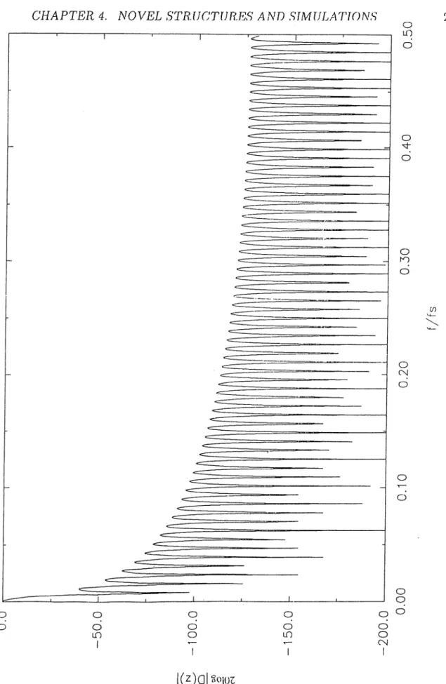
The linear phase characteristic, small size and good performance makes this lilter an atti’active clioice. The magnitude of the transfer function of the filtei' for around the signal band is given in Fig. 4.5 where O SR is oversampling period and u is the value of a in D{z). The overall shape is given in Fig. 4.4. For the liardware implementation, both MR and HR tyjres can be chosen. Both of them consume almost tlie same chip area, but HR implementation has an additional advcintage. Assume that oned^it stream coming from the modulator is pushed into a F'lFO-type shift register chain. The control logic can easily Ire constructetl in order to implement a sinc^ filter which has any desired power of two in place of n in Eq. 4.6. Since the output is ready in every clock c>cle, any desired decimation value can be picked. These two details are specifically important because they enable a variable resolution and speed exchanging mechanism, which makes the system suitable for a variety of resolution and speed requirements. A simplified block diagram of the filter is given in Fig. 4.3.
Tlie only jrroblem with the filter is that it has a tiny attenuation towards the end of the signal band. Usually this is not so important. If it is, the chip can be jrrogramed to another sinC filter for the flat response and a lower decimation value, so that the second stage filtering can be implemented. Another solution to this problem may be using a deemphasis [16] type second stage filtering which compensate, the attenuation. But, as explained previously this consumes quite a large chip area.
CHAPTER 4. NOVEL STRUCTURES AND SIMULATIONS 26
384 * 1-bit shift registers
CHAPTER 4. NOVEL STR.UCTIJRES AND SIMULATION!^ o o LO oo oLO o o o CN 27 0) l( z ) a |s c w
CHAPTER 4. NOVEL STRUCTURES AND SIMULATIONS 28 0.001 0
P a s sb a n d of D(z)
0.0015 0.0020 f/fs 0.0025 0.0030CHAPTER 4. NOVEL STRUCTURES AND SIMULATIONS 29
4.3
L im its and C om parison
The performance of the suggested system will be evaluated in two parts. First, the performance of the modulator is examined then the performance of the whole system is tested. For the testing of the modulator, a sine function in time domain, truncated with a heuristic non-rectangular windowing function to 4096 points is used foi' evaluation. The major part of the behavioral level simulation program is given in the appendix. The model of the modulator result a resolution of 102 dB which is equivalent to 17 bits. However, such a resolution has never been reported up to now for the best of our knowledge. Imr the second order conversion the best resolution re.|:)orted so far is below 100 dB [3]. Main reason of this should be the internally generated noise became more dominant after a certain limit. The output spectrum of the modulator liltered by an almost ideal filter is given in Fig. 4.6.
The output spectrum sliows that there is no harmonic distortion. The third harmonic distortion is usually decreases the resolution in most of the second order systems [4].
For the overall system ].)erformance the sine filter is replaced with our svkA filter for testing the performance of the suggested filter. A decimator of 128‘^‘ order is coitnected to the output of the filter in order to take into account the aliasing problem. The system is tested for stability fo]· various iii])uts and mismatch problems. For the resolution of the system several sine waves are applied to the input. For all of these inputs, the resolution was gieatcir than 96 dB, which is the required resolution for 16-bit output. An exam|)le output spectrum is given in Fig. 4.7. For the mismatch problems various coefficients of the suggested filter and previously reported filters cire tested up to 1% mismatch. The results show that, when sensitivity of most sensitive coefficients are compared the new filter performs better. Usually 1% mismatch causes drastic performance degradation or instability for other systems.
Higher resolution second order sigma-delta converters require highei' over- sampling rates. However, since the increasing oversampling value causes quite large increase in the chip area, they have not been cost efficient up to now. Consequently, even though the internally generated noise, is reduced and higher resolutions are made possible a technology which can use 1-micron devices ma.y be necessary for implejnentation in a reasonably small area.
Output spectrum of the suggested system is sufficiently good to satisfy the specifications for almost all the applications. The most important limitation
CHAPTER 4. NOVEL STRUCTURES AND SIMULATIONS 30 CO UT) I o IT) o o CsJ
CHAPTER 4. NOVEL STRUCTURES AND SIMULATIONS 31 c q d q Q lO I cn M— q q q d d d o LO o T— CM O o q d o iO o q d o CNJ o o o o q o o o o q CD
CHAPTER 4. NOVEL STRUCTURES AND SMULATIONS 32
is the speed. The speed limitation of the .system is unfortunately inherent for any oversampling data converter. Consequently, these converters will always be slow, they can be made faster but still they will be slow with respect to other converters using the same technology.
The system does not suffer from the non-monotonicity and the differential non-linearity. There may be small offset or gain errors but they are not signif icant because the feedback compensates most of them. However, there is an additional error source inliereiit in sigma-delta converters. The system oscil lates for certain DC input values resulting discrete noise tones at the output. This is caused by the finite impulse response window of the decimation filter. Although the 1-bit output sequence of the modulator is ¡periodic, the output of the filter is not a constant value unless an integer multiple of the period is not e(|ual to the window size of thii filtiu;. t ’sually tliose. tones .are not im’porta’it
nevertheless they increase the idle noise when there is only a DC input. This is called tlie idle channel noise.
4.4
E x p e cte d size and co m p lex ity
As mentioned above, only six sampling devices, an adding device for the loop filter, two switches for digital to analog conversion and a comparator consti tute the analog section of the system. In comparison to the previously reported double loop system in switch capacitor form, this can fit in O.TmnP with suf ficiently good noise performance [3]. It may be much smaller if the current mode implementation will be successful.
The digital section is the implementation of the decimation filter
D{z) = - 3 2 - ' “ + 32-’“
-38-1
- 32-> + 32-2 (4.13)
equivalently
o(n) = 3o(n —1)—3o(n —2 )+ o (n —3)-|-j/(?i)-32/(?r—128)-f 37/(n—2.'56)—2/(71 —384)
(4+4)
Summation of l-bit input values can be performed with combinational logic and the rest is summed up by a two stage structure utilizing 3 twenty-two-bit adders. The system require 4 twenty-two-bit registers to store o(i) values and
CHAPTER 4. NOVEL STRUCTURES AND SIMULATIONS 33
384 one-bit shift registers to store y(i) values. A shift register can be built with 6 transistors and a 22-bit very fast adder, using carry lookahead and carry select structure, can be built with 900 transistors. There is no bus and no interconnection problem. Everything is performed repeatedly, thus the control logic only determines the time when the output is to be changed. The control of the analog section is achieved by just a single flip-flop. The programability only adds 8 digital switches to the system. When we added u]) all of them, the number of digital transistors is slightly more than -5000. According to our ])ast experience this requires no more than (vrniV in 1.5 — //. technology.
Only remaining elements are clock drivers. So totally Im iiV is sufficient for the whole system. This is so small that it can be integi’ated in another chip for single chip multi purpose designs, or a few number of them can be integrated
ill a siiigie cliip.
This expected size is smaller than the any previously reported converters with these specifications. These ad\-antages mcd<es the system very suitable for fabrication, and the prograimdjility gives it a wide range ol a])|jlication areas.
C h apter 5
C O N C L U S IO N
in this thesis a new iinpleinentatiun ol second order sigiria· delta, conversion is ¡^resented. The discu.ssion starts with a summary of major advantages of sigma- delta modulation technique; then first and second order sigma-delta converter structures are described; their performance and noise shajung functions of the modulators are estimated theoretically. Other sigma-delta converter structures and their difficulties in applications are discussed. Then, a new structure which attains the jjerformance of the second order modulatoi' with a. single feedba.ck loop is proposed. Since, this modulator uses sma,ller number of components with respect to previous ones, it consumes less area. The performance of the modulator is estimated with a behavioral level simulation jrrograms and found to have a resolution of 17-bits which is higher than any previously reported values.
Then mismatch problems and robustness of the modulator is tested and comjjarecl with standard modulators using the same simulation idea. For the robustness we obtain the result that the worst case behavior of the new mod ulator is also better than the worst case behavior of previously reported ones.
Finally an improved HR decimation filtei· which can fit in a very small chip area is considered. The filter output has the. resolution of 16-bits and furthermore it is programmable to have a different resolution and decimation values. These features of the system brings a wide range of application ai'eas. Some of these are given below •
• Digital audio systems such as DAT, CD recorders, mini discs etc: Both the speed and the lesolution is adequate, even higher quality such as 18 bit systems can be constructed.
CHAPTER 5. CO N CL US I ON 35
• Biomedical signal processing such as ECG: Very slow signals with high resolutions are reciuired.
• Telephone, networks: 4KHz bandwidth and 13 bit resolution is required, so smellier chip satisfies all. In a single chip 4 channel coding doicoding can be implemented.
• Sonar signal processing: Very slow signal with high resolution is required. Implementation .should be static so a bit larger area is required.
• Single chip signal processors: Especially speech signals can be input and applications which require security such as LPCIO [18] or CELP [19] coder- decoders can be iabricated in just one chip.
5.1
Future Work
The rolnistness of the suggested system sliould be tested in circuit level with an cictual systein. Tins test should be ca,rried out for various im])lementations. The major variations should be determined and precautions should be delined.
There are a lot of ways to imjrrove the performance of sigma-delta, convert ers. The first one is the use better noise shaping functions so that the same resolution can be obtained \'dth lower oversampling rates. There is a lot of work going on for that purpose but unfortunately they only bring small con tributions: of course the tojric. of inteiest will be concentrated on this subject.
At the same time better single stage linear phase filters should be investi gated. This is especially important for optimizing the system performance.
Finally, the major problem, w'hich is the speed limitation, of sigma-delta converters can be made less significant by using special technologies such as BiCMOS. If bipolar technology is used in analog part the speed can be in creased by a factor of 10. Furthermore two different chips can be designed one doing analog filtering, one doing digital filtering. CaAs flash converters are reported to work at 4 GHz conversion rate so if Ga.As is used for analog circuitry, conversions such as 16 bits at lOMHz ma.y be possible for sigma-delta conversion. Certainly the feasibility of such converters should be investigcited.
A p p en d ix A
B eh avioral L evel Sim ulation P rogram
program SINGLE_LOOP_S£COND_ORDER_SIGMA_DELTA_CONVERTER; uses graph,crt; const FIR_filter_len=8192; num_of_out=1024; outfile='out.m'; decimation=128; ■type_of _f iltering= ’ H R ' ; var count,write_pointer,gm,gd,out_points,filter_len:integer; z n ,zn_l,zn_2,zn_3,clock,s:longint; samp_in,samp_in_l,qn,qn_l,qn_2,d;real; y:array [0..FIR_filter.len]of integer; c:array [0..FIR_filter_len]of integer; out_file:text;
pa:string[10];
{ Variables zn ---- > output of the H R decimation filter qn ---- > qn is q[n] in Fig 3.2
y ---> y[write_pointer] is y[n] in Fig 3.2
c ---> is the coefficient array of FIR filter
n_l---> denotes n-1
samp_in---> input sampling devices
}
APPENDIX A. BTN-IAVIORAL LEVEL SIMULATION PROGRAM 37
{Generate FIR Filter Coefficients} procedure gen^coef;
const scale=32000; begin
filter_len:=FIR_filter_len; s : =0;
for count:=0 to filter_len do if count=filter_len/2 then begin c [count] :=scale end else begin d :=(count-FIR_filter_len/2)*pi/128; d:=scale*sin(d)/d; c [count] :=round(d*(1-abs(count-filter_len/2)/filter_len)) {The above line stands for the windowing function}
s : =s + c [count]; end;
end ;
{Initialize Required Variables} procedure init;
begin clrscr;
if type_of_filtering=^IIR^ then filter_len:=381; clock:=0; write_pointer:=0; out_points:=0; z n_1:=0; z n _ 2 :=0; z n _ 3 :=0; qn:=0; s a j t i p _ i n _ l : = 0 ; q n _ l : = 0 ; q n _ 2 : = 0 ; c o u n t : = 0 ;
for count:=0 to filter_len do begin
y [ c o u n t ] : = 0 ; end ; g d : = d e t e c t ; g m : = 0 ; pa: = ^ i n i t g r a p h ( g d , g m , p a ) ; a s s i g n ( o u t _ f i l e , o u t f i l e ) ; r e w r i t e ( o u t ^ f i l e ) ; w r i t e l n ( o u t _ f i l e , ^ x = [ 0 ; e n d ; { S a m p l e t h e I n p u t } p r o c e d u r e s a m p l e ; b e g i n c l o c k : = c l o c k + l ; s a m p _ i n : = s i n ( 2 * p i * c l o c k / n u m _ o f _ o u t ) - 2 * y [ w r i t e _ p o i n t e r ] ; s a m p _ i n : = s a m p _ i n / 5 ; w r i t e _ p o i n t e r : = ( w r i t e _ p o i n t e r + l ) mod f i l t e r _ l e n ; e n d ; { I n t e g r a t e t h e Sampl e d S i g n a l s } p r o c e d u r e i n t e g r a t e ; b e g i n q n : = 2 * q n _ l - q n _ 2 + 2 * s a m p _ i n - s a m p _ i n _ l ; { q n _ l and q n _ 2 a r e two s a m p l i n g d e v i c e s o f o u t p u t } s a m p _ i n _ l : = S2Lmp^in; q n _ 2 : = q n _ l ; q n _ 1 : = q n ; e n d ;
APPENDIX A, BEHAVIORAL LEVEL SIMULATION PROGRAM 38
{ Q u a n t i z e t h e I n t e g r a t o r O u t p u t } p r o c e d u r e q u a n t i z e ; b e g i n i f qn >0 t h e n b e g i n y [ w r i t e _ p o i n t e r ] : =1 end e l s e b e g i n y [ w r i t e _ p o i n t e r ] : = - l ;
APPENDIX A. BEHAVIORAL LEVEL SIMULATION PROGRAM 39 end ; end; { C a r r y o u t H R F i l t e r i n g } p r o c e d u r e i i r ; b e g i n z n : = 3 * z n _ l - 3 * z n _ 2 + z n _ 3 + y [ w r i t e _ p o i n t e r ] ;
zn:=zn-3*y[(write^pointer-i-filter_len”128) mod filternden]; z n :=zn+3*y[(write^pointer+filter_len-256) mod filter_len]; z n :=zn-y[(write_pointer+filter_len-384) mod filter_len]; zn_3:=zn_2; zn_2:=zn_l; zn_l:=zn; i f ( c l o c k mod d e c i m a l i o n = 0 ) and ( c l o c k > f i l t e r _ l e n ) t h e n b e g i n o u t . p o i n t s : = o u t _ p o i n t s + 1 ; ■ p u t p i x e l ( o u t . p o i n t s , 1 7 0 + z n d i v 1 0 0 0 0 , w h i t e ) ; w r i t e l n ( o u t . f i l e , z n : 1 2 ) ; end ; end ; { C a r r y o u t F I R F i l t e r i n g } p r o c e d u r e f i r ; b e g i n i f ( c l o c k mod d e c i m a l i o n = 0 ) and ( c l o c k > f i l t e r . l e n ) t h e n b e g i n d : = 0 ; f o r c o u n t : = 1 t o f i l t e r . l e n do b e g i n
gd:=(write.pointer-count+filter.len) mod filler.len; d :=d+c[count]*y[gd]; end ; o u t . p o i n t s : = o u t . p o i n t s + 1 ; putpixel(out.points,170+round(d/10000),white); writeln(out.file,d : 12); end end ;
APPENDIX A. BEHAVIORAL LEVEL SIMULATION PROGRAM 40 { M a i n B o d y o f t h e P r o g r a m } b e g i n i f t y p e _ o f _ f i l t e r i n g = ^ F I R ^ t h e n g e n _ c o e f ; i n i t ; r e p e a t s a m p l e ; i n t e g r a t e ; q u a n t i z e ; i f t y p e _ o f _ f i l t e r i n g = I I R ^ t h e n i i r e l s e f i r ; u n t i l o u t _ p o i n t s = 1 0 2 4 ; w r i t e l n ( o u t . f i l e , ^ ] ; ' ) ; c l o s e ( o u t . f i l e ) ; e n d .
R eferen ces
[1] V. Friedman “Over.sarn]r]ed data conversion teclmiques,” lEEFJ Circuits
and Devices, vol. 6, pp. 39—'15, November 1990.
[2] D. .J. Goodman “The a|jplication of delta modulation to analog to digital pcm encoding,” Bell Syste.in 'I'pch., pj·). 321-343, 1969.
[3] B. P. Brandt, D. E. VVingai'd, and B. .A,. Woolej' “Second-order sigma- delta moduhition fo]' digital audio signal acquisition,” IEEE Journal of
Solid-State Circuits, vol. 26, pp. 618-627, April 1991.
[4] S. R. Norsworthy, I. G. Post, and H. S. Fetterman “A 14-bit 80-khz sigma-delta A/D converter; Modelling, design and performance evalua tion,” IEEE Journal of Solid-State Circuits, vol. 24, pp. 256-266, April 1989.
[5] L. Richard Carh-_v “A noise shaping coder topology for 15-f- bit converters,”
IEEE Journal of Solid-State Circuits, vol. 24, pp. 267-273, April 1989.
[6] E. B. Boser and B. A. VVooley "The design of sigma-delta modula tion analog-to-digital converters,” IEEE Journal of Solid-State Circuits, vol. 23, pp. 1298-1308, December 1988.
[7] Y. Matsuya, K. Uchiraura, A. Iwata, and T. Kaneko “A 17-bit over- sampling D-to-A conversion technology using multistage noise shaping,”
IEEE Journal of Solid-State Circuits, vol. 24, pp. 969-975, August 1989.
[8] Koch “A 12-bit sigma-delta analog to digital converter with 15 mhz clock rate,” IEEE Journal of Solid-State Circuits, SG. 21, pp. 1003-1009, De cember 1986.
[9] C. H. Giancarlo W. Scott, W. Lee and C. G. Sodini “Gmos implementation of an imediately adapti ve delta modulator,” IEEE Joxmial of Solid-State
Circuits, vol. 21, pp. 1088-1095, December 1986.
REFERENCES 42
[10] Phillip E. Allen Randall L. Geiger and Noel R. Strader. VLSI Design
Techniques for Analog and Digital Circuits. McGraw Hill, 1990.
[11] G. Pretzl D. Seitzer and N. A. Hamdy. Electronic Analog to Digital Con
verters. VViley-interscience, 1983.
[12] Michael .J. Dernier. High-speed Analog to Digital Convertion. Accidemic Pres.s, Inc, 1991.
[13] R. Gray “Spectral analy,sis of qauntization noise in a single-loop sigma- delta modulator with dc input,” IEEE Trans, on Coimmications., vol. 37, pp. 588-599, .June 1989.
[14] R. Gray “Spectral analysis of qauntization noise in a single-loop sigma- delta modulator with sinusoidal in])uts,” IEEE Trans, on Coinunications.., vol. 37, pp. 956-968, September 1989.
[15] R. Gi'ciy “Oversampled sigma-delta modulation,” IEEE Trans, on Comu-
nications., vol. 35, pp. 481-489, 1987.
[16] V. Friedman, D. M. Brinthaupt, D.-P. Chen, T. W. Deppa, .J. P. Elward, .Jr., E. M. Fields, .J. W. Scott, and T. R. Viswanathan “.A dual-channel voice-band PCM codec using SA modulation technique,” IEEE Journal
of Solid-State Circuits, vol. 24, pp. 274-280, April 1989.
[17] .J. G. Candy “Decimation for sigma-delta modulation,” IEEE Trans, on
Comunications., vol. 34, pp. 72-76, 1986.
[18] Hcilil PADJR. An LPC Vocoder System. PhD thesis, METU, 1983.
[19] V.Cuperman B.S. Atal and A. Gersho. Advances in Speech Coding. Kluwer Academic Publishers, 1991.

![Figure 2.3: Ba.sic Structure of 3-bit Charge Redistribution Converter a])])roa.ch is that it does not require digital to analog converter](https://thumb-eu.123doks.com/thumbv2/9libnet/5911832.122529/17.945.104.846.185.638/figure-structure-charge-redistribution-converter-require-digital-converter.webp)