MRI COMPATIBLE LEAD DESIGNS
FOR
IMPLANTABLE MEDICAL DEVICES
A THESIS
SUBMITTED TO THE DEPARTMENT OF ELECTRICAL AND
ELECTRONICS ENGINEERING
AND THE INSTITUTE OF ENGINEERING AND SCIENCE
OF BILKENT UNIVERSITY
IN PARTIAL FULFILLMENT OF THE REQUIREMENTS
FOR THE DEGREE OF
MASTER OF SCIENCE
By
Ahmet Ermeydan
September, 2007I certify that I have read this thesis and that in my opinion it is fully adequate, in scope and in quality, as a thesis for the degree of Master of Science.
Prof. Dr. Ergin Atalar (Supervisor)
I certify that I have read this thesis and that in my opinion it is fully adequate, in scope and in quality, as a thesis for the degree of Master of Science.
Prof. Dr. Ayhan Altıntaş
I certify that I have read this thesis and that in my opinion it is fully adequate, in scope and in quality, as a thesis for the degree of Master of Science.
Prof. Dr. Nevzat G. Gençer
Approved for the Institute of Engineering and Sciences:
Prof. Dr. Mehmet B. Baray
ABSTRACT
MRI COMPATIBLE LEAD DESIGNS
FOR
IMPLANTABLE MEDICAL DEVICES
Ahmet Ermeydan
M.S. in Electrical and Electronics Engineering Supervisor: Prof. Dr. Ergin Atalar
September, 2007
It is currently estimated that 600,000 cardiac pacemakers are implanted per year worldwide. It is expected that the usage of other stimulators such as deep brain stimulators (DBS) will reach this number in a short period. On the other hand, 2,000,000 MRI examinations are carried out each year worldwide and usage of MRI is expected to increase.
Unfortunately, people with metallic implants have significant risks in the MRI scanners. It is known that radio frequency and gradient fields of the MRI scanners may induce harmful currents on the implant leads. Radio frequency pulses may cause excessive heating and burns. In addition to this, time-varying gradient magnetic field induced currents on the leads can cause nerve stimulation. In case of cardiac pacemakers, this nerve stimulation may cause cardiac arrest.
In this thesis, novel MRI compatible lead designs were proposed. Lead designs are presented to ensure safe magnetic resonance scanning of patients with active metallic implants such as pacemakers, neurostimulators, and implantable cardio defibrillators. Semiconductor components such as transistors and diodes are used to prevent these undesired induced currents on the implant leads. Circuits on the implants are designed such that while the induction of currents is prevented, the desired signal transmission in between the implanted pulse generator and the body part is maintained.
The designs were tested by using experiments and computer stimulation. It was seen that the new techniques are effective in making MRI safe implantable devices. Benefits and problems of each design will be discussed in this text. It is believed that using this or similar techniques, patients with the implants will be able to be examined safely in MRI scanners.
ÖZET
VÜCUDA YERLEŞTİRİLEBİLİR MEDİKAL CİHAZLAR
İÇİN
MRG UYUMLU KABLO TASARIMLARI
Ahmet ErmeydanElektrik-Elektronik Mühendisliği, Yüksek Lisans Tez Yöneticisi: Prof. Dr. Ergin Atalar
Eylül, 2007
Bugün, dünyada senede 600.000 kalp pili takıldığı tahmin ediliyor. Diğer uyarıcı pillerin kullanımının, örneğin derin beyin uyarıcıları, kısa bir sürede bu rakamı yakalaması bekleniyor. Bununla birlikte, tüm dünya çapında senede 2.000.000 MRG kullanımı gerçekleştirilmekte ve MRG kullanımının daha da artması beklenmektedir.
Ne yazık ki vücuduna metalik cihazlar takılı insanlar MRG cihazları içinde çok ciddi risk altındadırlar. MRG cihazlarının radyo frekansları ve gradyan alanları vücuda yerleştirilen cihazların kablolarında zararlı akımların oluşmasına sebep olabiliceği biliniyor. Radyo frekansı sinyallerinden kaynaklanan en önemli risk fazla ısınma ve yanıktır. Buna ek olarak, gradyan alanlar da istenmeyen sinir uyarımlarına sebep olabilir. Kalp pili takılı hastalarda bu uyarım kalbin aniden durmasına sebep olabilir.
Bu tez çalışmasında, MRG uyumlu vücuda yerleştirilebilir kablo tasarımları geliştirdik. Kalp pilleri, siniruyarıcıları, kalp defibrilatörleri gibi aktif metalik vücuda yerleştirilebilir cihazlar taşıyan hastaların güvenli bir şekilde manyetik rezonans görüntülemesi yapılabilmesi için kablo tasarımları yapıldı. Vücuda yerleştirilen cihazların kablolarında meydana gelen bu istenmeyen akımları engellemek için yarı-iletken elemanlar örneğin transistörler ve diyotlar kullanılabilir.
İstenmeyen indükleme akımını engelleyecek ve darbe üreteci ile vücut dokusu arasında sinyal iletimini devam ettirecek şekilde vücuda yerleştirilebilir cihazların devreleri tasarımlandı.
Bu tez içerisinde geliştirilen tasarımlar deneyler ve simülasyonlar ile denendi. Tasarımların MRG uyumlu vücuda yerleştirilebilir cihazlar yapmak için etkili olduğu görüldü. Her bir tasarımın faydaları ve olası problemleri bu yazıda tartışıldı. Yakın bir gelecekte, bu tezde bahsedilen yöntemler veya benzeri tekniklerin kullanılması ile vücuda yerleştirilmiş elektronik uyarıcı taşıyan hastaların güvenli bir şekilde MRG cihazlarında çekimlerinin yapılacaktır.
ACKNOWLEDGEMENTS
I wish to express my deepest gratitude to my supervisor Prof. Ergin Atalar. With his knowledge, he has been a very helpful supervisor. During my M.S. study, I learned a lot about Magnetic Resonance Imaging and fundament of electronics with the guidance of Dr. Atalar. I am very grateful for his support and patience during my M.S. study. In my future life, I will always remember his support and contribution.
I would also like to thank my friends; Yiğitcan Eryaman, Halise Irak, Elif Aydoğdu, Onur Taşcı, Haydar Çelik and professors; Ayhan Altıntaş, Vakur Ertürk, Bülent Özgüler, Nail Akar, Ezhan Karaşan, I would like to thank them for their kind support. I thank Prof. Dr. Nevzat Gencer for taking part in my jury.
I would like to thank to my parents and my wife. Their presence was the biggest motivation for me everyday of this study. My wife, Esra Ermeydan actively contributed the experiments I’ve
conducted. Without her it would have been impossible.
TABLE OF CONTENT
1.
INTRODUCTION ... 1
2. BACKGROUND ... 6
2.1IMPLANTABLESTIMULATOR... 6 2.2MECHANISMOFHEATING ... 103. DESIGN ... 13
3.1ACTIVELEADS ... 133.2DIODERESISTORCIRCUIT(DRC) ... 14
3.3TRANSISTORDIODECIRCUIT(TDC) ... 19
3.4CAPACITORSWITCHCIRCUIT(CSC) ... 24
4. SIMULATIONS ... 29
4.1PARTI:PACINGPULSEMODELS ... 29
4.1.1 DIODE RESISTOR CIRCUIT (DRC) ... 29
4.1.2 TRANSISTOR DIODE CIRCUIT (TDC) ... 30
4.1.3 CAPACITOR SWITCH CIRCUIT (CSC) ... 35
4.2PARTII:INDUCEDVOLTAGESIGNALMODEL ... 37
4.2.1 DIODE RESISTOR CIRCUIT (DRC) ... 37
4.2.2 TRANSISTOR DIODE CIRCUIT (TDC) ... 37
4.2.3 CAPACITOR SWITCH CIRCUIT (CSC) ... 38
4.3PARTIII:EFFICIENCYMODELOFCSC ... 40
5. EXPERIMENTS ... 45
5.1HEATING MEASUREMENTEXPERIMENTS ... 45
5.1.1 COMPARISON OF WIRE HEATING WITH AND WITHOUT RF BLOCKING ELEMENTS (RFBE) ... 45
5.1.2 DIODE RESISTOR CIRCUIT (DRC) ... 48
5.1.3 CAPACITOR SWITCH CIRCUIT (CSC) ... 50
5.2NERVESTIMULATIONEXPERIMENT ... 54
5.2.1 CAPACITOR SWITCH CIRCUIT (CSC) ... 54
6. RESULTS ... 58
6.1HEATMEASUREMENTEXPERIMENTRESULTS ... 58
6.1.1 COMPARISON OF WIRE HEATING WITH AND WITHOUT RF BLOCKING ELEMENTS (RFBE) ... 58
6.1.2 DIODE RESISTOR CIRCUIT (DRC) ... 62
6.1.3 CAPACITOR SWITCH CIRCUIT (CSC) ... 62
6.2NERVESTIMULATIONEXPERIMENTRESULTS ... 64
6.2.1 CAPACITOR SWITCH CIRCUIT (CSC) ... 64
7. DISCUSSIONS ... 65
8. CONCLUSION ... 69
LIST OF FIGURES & TABLES
Figure 1. Illustration of main structure of the IPG. 6 Figure 2. Illustration of unipolar, bipolar and multielectrode leads. 8 Figure 3. (a) Simplified diagram of stimulator output stage for unipolar pacing mode; (b) Simplified diagram of stimulator output stage for bipolar pacing mode. 9 Figure 4. Simplified diagram of mechanism of electrode heating. 12 Figure 5a. Unipolar pacing mode DRC implementation with capability of programming positive pulses 14 Figure 5b. Unipolar pacing mode DRC implementation with capability of programming positive and negative pulses. 14 Figure 6. Bipolar and unipolar pacing mode DRC implementationwith capability of programming positive and negative pulses. 17 Figure 7. Multi electrode pacing mode DRC implementationwith capability of programming positive and negative pulses. 18 Figure 8. TDC implementation 19 Figure 9. Bipolar and unipolar pacing mode TDC implementation-1 with capability of programming positive and negative
pulses. 21
Figure 10.Multi electrode pacing mode TDC Implementation-1 with capability of programming positive and negative pulses. 22 Figure 11. Unipolar and bipolar pacing mode TDC Implementation-2 with capability of programming positive and negative
pulses. 23
Figure12. Multi electrode pacing mode TDC Implementation-2 with capability of programming positive and negative pulses. 24 Figure 13a. CSC (Parallel Capacitor) implementation 25 Figure 13b. CSC (Series Capacitor) implementation 26 Figure 14. Simulation result of DRC on electrode tissue impedance 30 Table 1. 5Spice PMOS and NMOS Characteristic Data 31 Table 2. Spice Model parameters definitions and units of MOSFETS 33 Figure 15a. Simulation result of TDC for unipolar pacing mode with positive pulse 34 Figure 15b. Simulation result of TDC for unipolar pacing mode with negative pulse 34 Figure 16. Simulation result of TDC for bipolar pacing mode 35 Figure 17a. Simulation result of CSC-parallel capacitor- for bipolar pacing mode 36 Figure 17b. Simulation result of CSC-series capacitor- for bipolar pacing mode 36 Figure 18a. Simulation result of CSC-parallel capacitor- on the electrode tissue impedance at 1 KHz 39 Figure 18b. Simulation result of CSC-parallel capacitor- on the ring tissue impedance at 1KHz 39 Table 3. Simulation result of DRC, TDC and CSC voltage measurement on the electrode and ring impedances. 40 Figure 19. The efficiency plot of CSC as a function of R1 41
Figure 20. The efficiency plot of CSC as a function of capacitance 42 Figure 21. The efficiency plot of CSC as a function of t1 43
Figure 22. The efficiency plot of CSC as a function of t2 43
Figure 23. Semi cylindrical phantom model. 46 Figure 34. Lead placement in the gel 47 Figure 35. Phantom and lead placement in the scanner 47 Figure 26. Lead model without RFBE used in the heating measurement 48
Figure 27. Lead model with RFBE used in the heating measurement 48 Figure 28a. Gel phantom setup with DRC 49 Figure 28b. Gel phantom setup with DRC 49 Figure 29a. IPG model without CSC 51 Figure 29b. IPG model with CSC 51 Figure 30a. Rectangular plastic phantom side 1 52 Figure 30b. Rectangular plastic phantom side 2 52 Figure 31a. Experiment setup without CSC 53 Figure 31b. Experiment setup with CSC 53 Figure 32. The Sciatic Nerve bundle where it leaves the vertebral column [27]. 54 Figure 33. Sciatic Nerve in thigh musculature [27] 55 Figure 34. Nerve muscle preparation of the frog leg 56 Figure 35. Nerve stimulation experiment setup 57 Figure 36. Temperature rise versus time at the distal and proximal electrode of a 20 cm wire without RF Blocking element 59 Figure 37. Temperature rise versus time at the distal and proximal electrode of the 20 cm wire 3.9 kΩ resistance placed on the distal electrode of the wire 59 Figure 38. Temperature rise versus time at the distal and proximal electrode of a 20 cm wire with PIN diode MA4P7452F-1072T placed on the distal electrode of the wire 60 Figure 39. Temperature rise versus time at the distal and proximal electrode of a 30 cm wire without RF blocking element 60 Figure 40. Temperature rise versus time at the distal and proximal electrode of the 30 cm wire 3.9 kΩ resistance placed on the distal electrode of the wire 61 Figure 41. Temperature rise versus time at the distal and proximal electrode of a 30 cm wire with PIN diode MA4P7452F-1072T placed on the distal electrode of the wire 61 Figure 42. Heating experiment result of IPG model with DRC 62 Figure 49. Heating experiment result of IPG model without CSC 63 Figure 44. Heating experiment result of IPG model with CSC 63
1. INTRODUCTION
With an increasing number of magnetic resonance imaging (MRI) examination and parallel growth in the number of implantable stimulators such as pacemaker, implantable cardioverter defibrillator (ICD) implants and deep brain stimulator (DBS), safety of MRI for the patient with these implants has become an important issue. In this thesis, novel implant designs that enable safe MRI exams are proposed.
More than 370,000 pacemakers and ICDs were implanted in the United States in 2003 [1]. According to Pennsylvania Health Care Cost Containment Council (PHC4), the number of MRI scans increased from 9.3 million to 13.5 million between 1999 and 2001 in USA. PHC4 indicated that 120000 MRI examinations were performed in Pennsylvania hospitals in 2003 [2]. According to these data, it is estimated 50-75% probability of a patient being indicated for an MRI over the lifetime of their device [3]. Magnetic resonance imaging utilizes three types of magnetic fields: static (also known as B0); radio frequency (RF); and
gradient magnetic fields.
The static magnetic field is a critical element in a magnetic resonance imaging system. It is designed to be very strong (0.1 tesla to 7 tesla and typically 1.5 tesla) and very uniform (in the order of 1 parts per million inhomogeneity within volume of interest).
In the MRI scanner, an RF magnetic field with the frequency of 42.58 MHz/T is generated by RF coils with the aim of exciting the spins that are magnetized by static magnetic field. The RF field is typically circularly polarized and perpendicular to the static magnetic field. The gradient fields are applied to encode signal generated by the excited spins. They also serve in the slice selection process. In the MRI scanners, there are three gradient fields. Using the combination of the x-, y- and z-gradient fields, a gradient field in any direction can be obtained enabling slice selection and encoding in any arbitrary direction.
Excessive heating in the presence of elongated metallic structures such as electrical wires, guidewires, and implant electrodes inside the body have been investigated by several researchers. Smith et al.[4] measured RF heating inside a 1.5T MRI scanner. In this gel-phantom study, the temperature increase was measured in different lengths of wires with 0.6 mm insulation while an SAR of 4.2 W/kg was applied to the body. The result of this study shows that the maximum temperature rise was measured as 16.82 °C at the end of the 40 cm wire.
Sommer et al. [5] conducted a study on twenty-one models of pacemakers and forty-four pacemaker electrodes in order to evaluate safety and feasibility of magnetic resonance imaging at 0.5 T in patients with implanted cardiac pacemakers. In vitro measurements of this study show that maximum temperature rise at electrode of the leads was measured as 8.90 °C at SAR of 0.6 W/kg. The temperature increased by 23.50 °C when SAR of 1.3 W/kg was applied. In vivo measurements were made with forty-four patients with implanted cardiac pacemakers. After 51 MRI examinations, none of the pacemakers displayed a dysfunction at MRI and no changes occurred in the programmed parameters.
Luechinger et al. [6] measured temperature rise in saline phantom at the electrodes for different types of pacing leads. The maximum temperature rise was measured approximately 13 °C for unipolar lead. Besides, in vivo experiments were performed in a pig. The maximum temperature rise was measured as 15 °C for a passive fixation lead and it was measured as 30 °C with screw in lead. No significant threshold or impedance changes of the leads were observed.
In one reported case [7], a patient with DBS became comatose after 15 minutes of diathermy. The RF magnetic field is used to heat tissue in this procedure. After this procedure, the patient was unresponsive and comatose condition was confirmed after neurological exams. Edema centered at the electrodes was showed in the MRI examination.
In another case [8], a thermocoagulation lesion adjacent to the electrode after MRI examination was observed on a patient with DBS system. The MRI examination was performed at 1 T with body transmit coil. But the manufacturer (Medtronic, Minneapolis, MN) specifies cautions for the MRI examination of a DBS patient and it is explained that head transmit coil with SAR less than 0.4 W/kg at 1.5 T should be used for DBS patients during MRI examinations.
Rezai et al. [9] measured RF heating with gel-phantom. The maximum temperature rise was measured as 25.3 °C with an average SAR of 3.9 W/kg and there is no loop in the lead for this measurement. On the other hand, the leads were positioned with two small loops that are approximately 2.5 cm in diameter in order to simulate a loop near the burr-hole cover for DBS lead placement. The temperature rise was measured as 6.1 °C at this condition.
Kainz et al. [10] was performed another study about heating of neurostimulating systems. The measurements were performed at 1.5 T and 3.0 T in the anatomical realistic and cubic phantoms. The temperature rise was measured as 2.1 °C at the electrode of the lead. It was concluded that reduction of the number of the loops at the IPG reduces heating associated in MRI examinations.
Bendadis et al. [11] performed experiments with 27 MRI examinations on 25 patients. 26 MRI scans were performed with head transmit coil, while one of them was performed with body transmit coil. One of the patient reported chest pain during MRI examination. This survey yielded no reports of discomfort around the lead or IPG excluding one case.
Dempsey et al. [12] investigated mechanism RF heating during MRI examination. It was concluded that resonant circuits with inductance and capacitance have significant heating potential. Thus extended wires also have potential for thermal injury.
There should be limitations to make safe MRI examinations and these criteria are defined by The United States Food and Drug Administration (FDA).These criteria are stated that during
MRI examination, SAR should be in the limit of 8 W/kg in the head and trunk; 12 W/kg in the extremities when averaged over a gram of tissue for 15 minutes. Also, temperature changes should be in the limit of 1 ˚C in the head, 2 ˚C in the trunk and 3 ˚C in the extremities [13]. Several strategies may be used to ensure safety in metallic implants. One of the basic methods is limiting the input RF Power. Determination of RF power threshold provides to specify reasonable amount of heating during MRI examination. Yeung et al. [14] presented a methodology for such a power limitation. However, many modern pulse sequences such as fast spin-echo or steady-state free precession (SSFP) require high RF power levels. Therefore there is no guarantee that good quality images can be acquired with this limitation.
Susil et al [15] presented usage of RF chokes in the design of a combined electrophysiology/MRI catheter. Besides, Ladd M.E et. al. [16] presented usage of triaxial chokes to present high impedance to currents flowing on the outer surface of the triax.
Implantable medical device incorporating integrated circuit notch filters was developed by Medtronic (Minneapolis, MN) [17], and pacemaker with EMI protection was developed by Telectronics [18]. These two designs provide to safety for electromagnetic interference to the implant. However, limitation of RF heating at the lead is not guaranteed. High current may still be flowing through long cables, which can cause excessive heating and burns. Biophan’s “photonic pacemaker” provides optical signal transmission in between the generator and the body part [19]; which provides safety [20]. Because there is no coupling with the optical system and the electromagnetic field, the conversion between electrical and optical systems has limited efficiency and therefore the lifetime of the pulse generator reduces significantly. The miniaturization of this system is also a difficult task.
Another possible safety problem with MRI is that gradient induced currents on the implants may cause undesired nerve stimulation with a possibility of cardiac arrest. A spinal fusion
stimulator was analyzed theoretically for this purpose [21] and although authors have noted a reduction in the stimulation threshold level change was not alarming. As will be discussed in this manuscript this conclusion is not inline with my experimental results.
As it will be explained more detailed in the next section, the active implants are composed of two parts: implantable pulse generator (IPG) and a lead. IPG has typically a metallic case and the lead is insulated with a plastic coating and the electrode of the lead is bare and touches the target organ. In some designs (bipolar leads), two wires are used in each lead. One of these wires is connected as ground and connects to a relatively large metallic ring. In some designs more than two wires are used and connected to a series of electrodes. Even in other designs, multiple leads are used. In this study, a novel method is proposed to make MRI safe active implanted devices. This method uses active circuit elements on the lead in order to make MRI safe lead. This new approach is not only easier to manufacture and miniaturize, but also more effective in reducing the induced currents than passive circuits such as choke inductors.
2. BACKGROUND
In this chapter, the necessary background for explaining the design of the MRI compatible implantable stimulators will be given.
2.1 IMPLANTABLE STIMULATOR
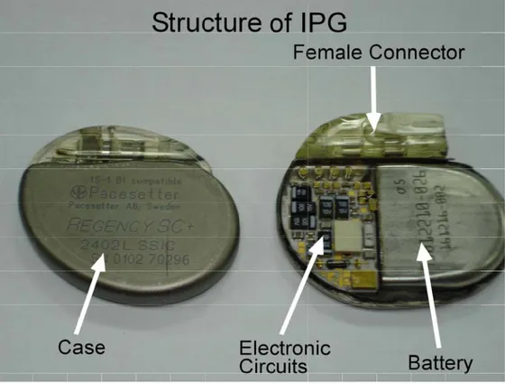
Implantable stimulators are composed of one implantable pulse generator (IPG) and one or more leads. Although IPG has different functionalities for different types of stimulators such as pacemakers, ICDs and DBS, general functionalities can be summarized as: (1) the creation of stimulation pulses on the target tissue; (2) the communication with a programmer which may be placed outside of body; (3) other functions like sensing. Structure of the IPG can be divided into four main parts: (1) electronic circuits; (2) battery; (3) female connector; and (4) case. This structure is illustrated in Figure 1.
In order to perform stimulation and sensing functions of IPG, there should be connection between IPG and target tissue. This connection is provided by the leads. Their mechanical structure varies with stimulator types. According to applied therapy, pacemakers and ICDs have two main types of leads; unipolar and bipolar (see Figure 2). The stimulators operating in unipolar pacing mode use only one wire in the pacing lead. In this method, the pacing pulse is transmitted by applying potential between the pacing lead and the case of the IPG (implantable pulse generator). The stimulators operating in a bipolar pacing mode use two wires in the pacing leads. In this method, one wire is used as the pacing signal and the other one is used as ground. For example, Kappa 900-KDR901 model of Medtronic pacemaker can operate in both bipolar and unipolar pacing modes, while Kappa 900-KDR906 model of Medtronic pacemaker [22] uses only unipolar lead. On the other hand, DBS and pain stimulators utilize multielectrode leads. Multielectrode leads typically have four or more electrodes (see Figure 2). A wide variety of current patterns can be obtained using these electrodes. Since the current applied to each of the electrodes can be modified independently, it is possible to obtain any combination of unipolar and bipolar pacing.
Figure 2. Illustration of unipolar, bipolar and multielectrode leads.
Note: Leads with a wide variety of lengths are provided by the manufacturers, typically in the ranges of 30cm to 80cm.
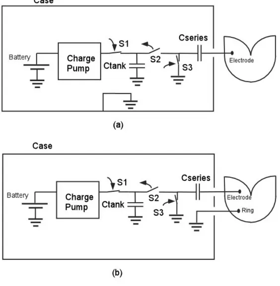
Modern stimulators have advance functionality in order to deliver programmable pulses. The output stage of a typical stimulator is shown in Figure 3. With the aid of this circuit stimulation voltage can be programmed from 0.2V to around 7.0V with pulse widths ranging from 0.1 ms to 2 ms. The typical stimulator battery voltage is in the range of 2 to 2.8 V. Since the pacing amplitude may be higher than battery voltage a charge pump with a tank capacitor is used in most IPGs. A series capacitor is placed in the circuit in order to null the total charge delivered to the tissue. This effect of nulling the total charge helps to overcome effect of ‘electrode polarization’, which is formed by accumulation of charges around the
electrode-tissue interface [23]. Tank and series capacitors are typically in the order of 10μF. The typical impedance seen at the electrode and tissue interface is in the range of 400 Ω to 1000 Ω [23]. Simplified diagram of stimulator output stage is illustrated in Figure3.
Figure 3. (a) Simplified diagram of stimulator output stage for unipolar pacing mode; (b) Simplified diagram of stimulator output stage for bipolar pacing mode.
For unipolar pacing, the ground of electronic circuits is connected to stimulator case (Figure 3a). During charging period, S1 and S3 switches are closed and S2 switch is open and tank capacitor is charged by the charge pump.
During stimulation period, S1 and S3 switches are open and S2 switch is closed the accumulated charges on the tank capacitor flows over the series capacitors to the tissue.
When the short stimulation period ends, the switches return back to original conditions, i.e. S1 and S3 switches are closed and S2 switch is open. In this period, the tank capacitor gets lost charges back from the charge pump, and in the mean time the charges accumulated in the series capacitor discharges toward ground. The operating principle of the bipolar pacing is very similar to the unipolar case. Only difference is that in the bipolar pacing, the ground of electronic circuits is connected to the tissue by the lead rather than the case (see Figure 3b).
Modern cardiac pacemakers also have important functionalities. One of the most critical functionality is sensing bioelectric signals from the cardiac muscle (intracardiac ECG). This function provides synchronous pacing and recording any abnormal cardiac activity. Besides, defibrillators also use sensing in order to detect fibrillation. Typical intracardiac ECG signal amplitude ranges from 0.2 mV to 3.2 mV in the atrium and from 0.4 mV to 6.4 mV in the ventricle [23]. The detection of these small signals requires amplification and filtering. The main network power (50 Hz in Europe and 60 Hz in USA) interfere with the intracardiac ECG signal. Other interference source is the electromyogram signal originating from the muscles around the pacemaker case. This electromyogram signal frequency range changes from 100 Hz to a few kHz. Since the energy of intracardiac ECG signal has significant components at low frequencies a 70 to 200 Hz pass-band filtering is applied in order to minimize the interference [23].
2.2 MECHANISM OF HEATING
In order to explain the proposed methods of preventing the excessive temperature rise at the electrode of the implant lead, a very brief explanation of the heating mechanism is given below.
In MRI, radio frequency (RF) pulses are applied to obtain echo from the sample of interest. The frequency of RF pulse is proportional with the strength of the main magnetic field,
which is approximately 64 MHz for a 1.5T MRI scanner. Magnetic fields are only required to obtain the desired echo, however, since it is not possible to uncouple electric and magnetic fields, some additional and unwanted electric field is generated in the body. The optimization process (the process of obtaining the desired magnetic field while minimizing the electric field) yields different results for different type of magnets. For a horizontal bore magnet, the optimum field distribution that minimizes the electric field while keeping the magnetic field uniform in the body is achieved by a special coil type called birdcage coil [24]. In a properly designed birdcage coil, electric field at the center of the object is zero and increases linearly in the radial direction, while electric field is oriented in the z-direction (along the axis of the magnet bore).
When a metallic implant is placed inside the body, the electromagnetic field may induce current on the wire. The worst conditions are when the lead is directed mostly in the z-direction and loops are formed by the lead.
Concentrating on one lead with one electrode case, electric and magnetic field in the body generates a potential difference between pacemaker case and the electrode. This voltage causes a current flow on the lead. This current typically is not high enough to cause heating of the wires of the lead but the current leaves cable at the electrode. High concentration of the current at the tissue adjacent to the electrode heats up significantly. Radio frequency currents may flow from lead directly to the body by the mechanism known as displacement current. In this mechanism, the lead insulation material acts as dielectric and high currents may still flow [4-9].
Calculation of the amount of heating at the tissue adjacent to the electrode is a complex procedure. It involves solution of an electromagnetic scattering problem in a lossy medium and also a bioheat problem in an inhomogeneous medium. Induced voltage on the stimulator experiences impedance which is combination of the electrode-tissue impedance,
lead impedance, lead-to-IPG case impedance, IPG to body impedance. In a typical implant design, these other impedances can be ignored. Induced current is determined by the electrode-tissue impedance (see Figure 4).
3. DESIGN
In this chapter, three different MRI-compatible lead designs are given.
3.1 ACTIVE LEADS
Here, the active leads have been proposed with the aims of reducing lead electrode heating problem. Three different implementations have been proposed: “Diode-Resistor Circuit”, “Transistor-Diode Circuit” and “Capacitor-Switch Circuit”.
In the first implementation, PIN-diode and resistor are placed in parallel on the pacing leads in order to reduce the induced current on the leads. Pacing energy is slightly reduced due to the finite turn-on voltage of the diode. However, induced radio-frequency current is reduced significantly since PIN diode acts as a high valued resistor at this frequency. The parallel resistor increases the leakage currents that alleviate the problem of charge accumulation at the electrode. This design can be used in both unipolar and bipolar pacing. Since both diode and resistor are incorporated in this circuit, we call the circuit “Diode-Resistor Circuit” (DRC).
In the second implementation, a resistor is placed in parallel to series combination of transistor and diode. They are placed on to pacing leads to reduce the induced current on the leads at radio frequencies (MRI application) and gradient fields. Similar to first implementation, this circuit enables pacing pulse to be transferred. However, the pacing energy is slightly reduced due to the finite turn-on voltage of the diode and turn-on resistance of the transistor. Induced currents, however, are blocked. This design is called “Transistor-Diode Circuit” (TDC) and can be used both unipolar and bipolar pacing modes. In the third implementation, resistors are placed on to pacing lead to reduce the induced current on the leads. Pacing energy is accumulated on a serial or parallel capacitor placed at the distal end of the lead and discharged to the target body part by the help of an electronic
switch. Since capacitor is changed with a very low current, impedance of the wire can be made very high. This circuit is called “Capacitor-Switch Circuit” (CSC).
The operating principle of the new approach is much simpler than passive circuits. The circuit can be miniaturized and therefore can be incorporated to flexible leads without a significant effort and cost.
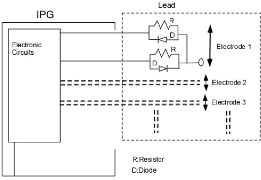
3.2 DIODE RESISTOR CIRCUIT (DRC)
In this implementation, parallel diode and resistor are added on to pacing leads to reduce the induced current on the leads. This implementation is seen in Figure 5.
Figure 5a. Unipolar pacing mode DRC implementation with capability of programming positive pulses
In this implementation, during pacing pulse, diode conducts the current after pacing pulse level passes diode’s turn-on voltage threshold level (typically 0.6V). Therefore, there is no significant change in the applied signal level. When the stimulator is exposed to radio frequency electromagnetic radiation, induced RF voltage on the lead would not cause excessive current at the electrode because of the diode and resistor. In the implementation of this design, PIN diode is used. PIN diodes’ characteristic is very suitable for this application. Although they behave like a regular diode at a low frequency signal such as pacing signal is applied to them, they act as a resistor at radio frequency (RF). Typically, their RF impedance is high (in the order of several kilo-ohms) when zero or negative bias is applied. Electrical properties of PIN diodes vary and can be obtained from their manufacturers’ data sheets.
One of the main characteristics of the Diode-Resistor Circuit is that in the normal operation, i.e., when IPG sends the pacing pulse, it causes only a small loss of power. On the other hand, it exhibits a resistance to radio-frequency signals. This resistance is a function of applied positive current. When no or negative voltage is applied to the diode, the RF resistance is in the order of several kilo ohms. This is very useful property in order to block induced current flow on the lead. In the proposed design, the parallel diode-resistor pair blocks the induced current flow.
Besides, standard stimulators use serial capacitor each lead. There are two significant reasons for the usage of this serial capacitance: (1) it provides safety condition to block DC current flow to the target body part in a fault condition; (2) it eliminates the possibility of electrode polarization due to null the total charge on the body by discharging the capacitor. In order to enable capacitor discharge, a parallel resistor is used in this implementation. The value of this parallel resistor must be chosen properly. If resistance is too high, capacitor
cannot be discharged during one pacing cycle and adversely affect the pacing capability of the design. On the other hand, if the resistance is too low, some RF current may flow on the resistor and therefore the safety performance of the lead design will diminish.
As described in Background section of this thesis, electrode tissue impedance can be selected as 1 kΩ. In the experiments of this thesis, a MACOM PIN Diode MA4P7452F-1072T was used. Its impedance is 3.5 kΩ. If the resistance of the resistor is selected as 10 times larger than impedance of diode, resistance value of the resistor can be ignored in the parallel combination of resistor and diode. Thus, a 50 kΩ resistor is very suitable for this application.
Modern pacemakers have two types of pacing pulse techniques: unipolar and bipolar. The method is selected based on the patient condition and illness. In unipolar pacing mode, pacing signal transmission between electrode and the case of the IPG is performed and this operation is controlled by the IPG.
Above mentioned design works only for positive unipolar pacing pulses. If negative pacing pulses are desired, the orientation of the diode may be reversed. However, if capability of programming both negative and positive unipolar pacing is desired, the design has to be modified as shown in Figure 5b.
In this design, two wires are necessary for each of the electrodes. While one of the wires is in use, the other is disconnected using an electronic switch. Using this method, programmable-polarity unipolar pacing can be obtained, while ensuring high resistance at RF frequencies in order to minimize induced lead currents.
In addition to this, in bipolar pacing mode, two electrodes are used at the same time during pacing sequence and case of the pacemaker is not used. One of the wires carries the signal from voltage source through the PIN diode and it reaches target body part. Then, this pacing pulse returns from body part to ground ring of the lead. This ring connected to IPG through
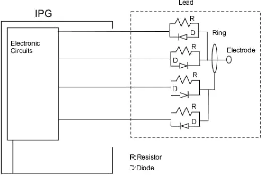
another wire with PIN diode and pacing pulse reaches the IPG through this wire. In order to create both positive and negative pacing pulses, there should be four wires and four PIN diodes in this implementation. This four-wire and one-electrode design support both unipolar and bipolar pacing modes if the electronic circuit at IPG contains switches that would relay the ground from the ring of the lead to the case of the IPG. Figure 6 shows this pacing configuration employing four independent wires with PIN diodes.
Figure 6. Bipolar and unipolar pacing mode DRC implementation with capability of programming positive and negative pulses.
On the other hand, Deep Brain Stimulators (DBS), Spinal Cord Stimulators (SCS) and Nerve Root Stimulators (NRS) have different stimulation technique rather than common electrical stimulation application such as cardiac pacing and defibrillators. In these simulators, multiple electrodes are used in order to generate complicated current profile in the body with the aim of providing maximum therapeutic benefits [25]. For example, typical DBS generators use four to eight electrodes in today’s technology. In these designs, similar to unipolar pacing mode, pulses are programmed independently for each of the electrodes
and the IPG case is used as ground. This capability enables bipolar pacing mode, where the pacing pulse is transmitted between two different electrodes by programming one of the electrode positive and the other electrode negative pulse voltage. The mode of operation and potentials applied to the electrodes are selected by the physician in order to obtain a successful therapeutic effect.
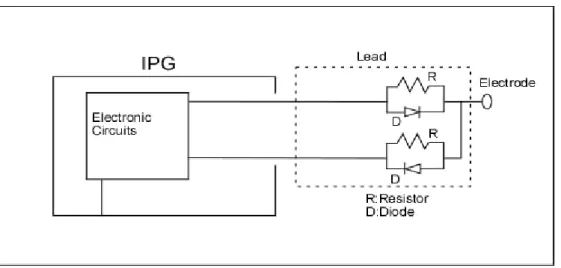
In order to achieve this desired mode of operation, the design has been modified such that each of the electrodes connected to two wires using a PIN diode and resistor pair as shown in Figure 7. Serial capacitors are placed on one of the wires of each electrode. Arbitrarily, these capacitors are placed on the wires that carry positive pulse. Alternatively, the capacitors can be placed on the negative current carrying wires. In order to provide MRI compatibility and the desired functionality of stimulators with multi electrode mode, electrodes of the stimulators are reconfigured as seen in Figure 7.
Figure 7. Multi electrode pacing mode DRC implementation with capability of programming positive and negative pulses.
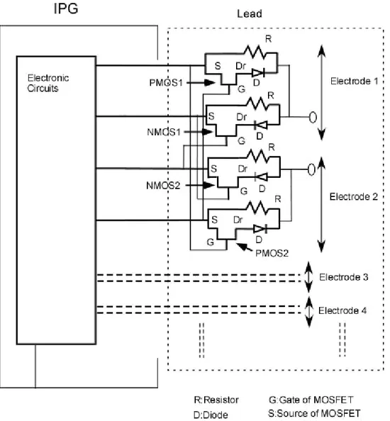
3.3 TRANSISTOR DIODE CIRCUIT (TDC)
In this implementation, resistor is placed in parallel to series combination of transistor and diode. This design not only eliminates induced RF currents but also minimizes gradient field induced currents. The implementation is in Figure 8.
Figure 8. TDC implementation
Although the transistor can be selected as BJT or MOSFET, in this thesis, the transistor was selected as a MOSFET transistor in order to increase efficiency and decrease power loss. Also enhancement-mode MOSFET is the most suitable model for this design. There are two different options for the diode selection. High frequency diode with high power durability or a PIN diode can be used.
When the pacing pulse is transmitted from IPG to target tissue, IPG opens MOSFET transistor by changing gate voltage of the transistor. At this condition MOSFET transistor is in the triode region and it behaves like a very small resistance. Pacing pulse level is adjusted greater than threshold voltage level of the diode. When the signal voltage level is higher than threshold voltage level of diode, current flows and the target tissue is stimulated.
One of the important advantages of this design over Diode-Resistor Circuit is that TDC does not only blocks induced RF currents but also induced low frequency currents. In this way, possible gradient-induced currents will also be blocked using this circuit.
In order to operate unipolar and bipolar pacing modes, two different implementations are made. In the first implementation, PMOS transistor is used when the positive pacing pulse is transmitted. Based on CMOS technology, very small resistance is obtained. PMOS transistors’ source to gate voltage difference should be significantly greater than source to drain voltage difference in order to obtain very small resistance that can be assumed to be short circuit. Thus, during pulse transmission, zero or negative voltages should be applied on the gate of the PMOS transistor and positive voltage should be applied on source of the PMOS transistor. By using this configuration, small resistance value is obtained during transmission of pacing pulse. Diode connection is adjusted based on positive pulse direction with PMOS transistor.
In addition to this, negative pulse transmission requires similar configuration. Therefore, NMOS transistor is used for this purpose. Based on CMOS technology, NMOS transistors’ gate to source voltage difference should be significantly greater than drain to source voltage difference in order to obtain very small resistance. Thus, during pulse transmission, required positive voltages should be applied on the gate of the NMOS transistor and zero or negative voltage should be applied on source of the NMOS transistor.
In order to use both unipolar and bipolar pacing modes, electrode of the stimulator is reconfigured and it is seen in Figure 9. However, a handicap exists for this implementation. During transmission of the pacing pulse, one of PMOS transistor should work and the other one should be closed. Similarly, one of NMOS transistor should work depending on selection of PMOS transistor.
Figure 9. Bipolar and unipolar pacing mode TDC implementation-1 with capability of programming positive and negative pulses.
In order to satisfy requirement of multiple functions of DBS, SCS and NRS, TDC implementation should be changed. Similar to Diode Resistor circuit, two wires are required to implement one electrode. In this model, when the one electrode transmits pacing pulse, other electrode cannot transmit any pacing pulse. Thus, two electrodes cannot transmit pulse at the same time. This situation limits some functional requirements but it satisfies many functional applications with ease of implementation. Configuration of multi electrodes lead is seen in Figure 10.
Figure 10.Multi electrode pacing mode TDC Implementation-1 with capability of programming positive and negative pulses.
The second implementation of this model was designed to provide flexibility to first implementation. In the first implementation, each electrode control depends on other electrode. Therefore, gate of the transistors are connected to the IPG and this increases the flexibility. IPG sets the gate voltage but this situation increase number of wires. This configuration is sketched in Figure 11.
Figure 11. Unipolar and bipolar pacing mode TDC Implementation-2 with capability of programming positive and negative pulses.
In multi electrode implementation of this model, each electrode directly controlled by IPG and it means that each electrode can transmit pacing at the same time. This implementation model increases number of wires. This situation can satisfy all functional requirements but it causes usage of more wires. Configuration is seen in Figure 12.
Figure12. Multi electrode pacing mode TDC Implementation-2 with capability of programming positive and negative pulses.
3.4 CAPACITOR SWITCH CIRCUIT (CSC)
In this implementation, when charging the capacitor, the connection between body part and capacitor is kept open. Capacitor is charged with the small current flowing on the resistors in the ideal period between two pace pulses. In order to pace, the accumulated energy on the capacitor is suddenly discharged on the body part. The duration of pacing pulse and the
frequency are programmed to the implantable pace generator by the physician to achieve desired treatment. Typically, while pacing frequency is on the order of one hertz, the discharging period is about 1 msec. This model is suitable for only bipolar pacing. The capacitor can be placed parallel or series to leads and PMOS transistor selected as a switch in this implementation. This implementation models are seen in Figure 13a and 13b.
Figure 13a. CSC (Parallel Capacitor) implementation
In this implementation, there is no additional control line. By using suitable transistor, pacing process is easily adjusted. However, this design may suffer from “electrode polarization” problem since the average current applied to the electrode is not zero.
Figure 13b. CSC (Series Capacitor) implementation
In this implementation, there is a control line in the lead. By applying suitable control voltage on the transistor, pacing process can be easily adjusted. Since there is a series capacitor in the circuit, “electrode polarization” problem does not exist.
In this implementation, capacitor and serial resistors values should be optimized, in order to find most power efficient conditions. Typically PMOS (MOSFET) transistors have very small resistance (in the order of 50Ω ), when transistor is on. Therefore, transistor effect was ignored in the efficiency calculation. During charging, some power dissipates on the serial resistors and some power transmits on the body part. In order to increase the IPG’s battery life, an efficient power transmission needs to be obtained. The power efficiency of this circuit can be obtained. In the following paragraphs, the efficiency equation will be obtained.
After system is used for several seconds, capacitor voltage charge and discharge waveform becomes periodic. We assume period starts at the end of the charging period. We assume this maximum capacitor voltage is
V
C2(0). When the switch is on, the capacitor dischargesover the electrode-tissue interface.
The voltage of the capacitor decreases during discharging period and reaches the value defined as
V
C1(0). The equation of capacitor voltage during charging can be written as:2
(0)
(
1(0)
)
11t R C
C s C s
V
=
V
+V
−
V
e
− (1)where, C is capacitance of capacitor,
t
1 is capacitor charging duration (on the order of 1sec); R1 is the total series resistance on the capacitor during charging period and Vs is the
battery voltage.
Similarly, the equation of capacitor voltage during discharging can be written as:
2 2 1
(0)
2(0)
t R C C CV
=
V
e
− (2)where, C is capacitance of capacitor,
t
2 is capacitor discharging duration (on the order of 1msec); R2 is the electrode-tissue impedance during discharging period.
During charging period of the capacitor, some power is dissipated on serial resistance (R1)
and equation of this dissipated energy on R1 can be written as:
(
)
2 1 2 1 2 2 1 2(0)
1
2
t t R C R C C sC
W
=
⎡
⎢
V
−V
e
−⎤
⎥
−
e
−⎣
⎦
(3)where, W1 is dissipated energy on serial resistance.
During discharging period of the capacitor, some power is transmitted on the body part (R2)
and equation of transmitted energy to body part can be written as:
(
2)
2 2 2 2 2(0) 1
2
t R C CC
W
=
V
−
e
− (4)where, W2 is transmitted energy to body part.
By using these two equations, efficiency equation of this system can be written as:
(
) (
)
(
)
(
)
(
)
1 2 1 2 2 1 1 2 1 1 2 2 2 2 2 11
1
1
1
t t R C R C t t t R C R C R Ce
e
W
W
e
e
e
η
− − −− +
−
=
=
−
−
(5)4. SIMULATIONS
In this chapter, in order to observe whether proposed designs satisfy expectations about pacing pulse transmission and RF current blocking, pacing pulse models and induced voltage models due to MRI simulations of three different MRI-compatible lead designs are done. Pacing pulse simulations, induced voltage simulations of three implementations and efficiency simulation of CSC are given in the following part.
4.1 PART I: PACING PULSE MODELS
Basic properties of simulations should be defined before simulation results will be given. In standard stimulator applications, pulse duration changes with the interval of 0.1ms to 2ms. In this implementation, pulse duration is applied as 1msec with the period of 1 sec. electrode-tissue impedance is assumed to be 1 kΩ. Pulse level is applied as 5 volt.
4.1.1 DIODE RESISTOR CIRCUIT (DRC)
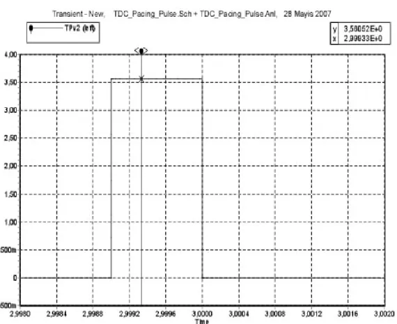
In order to simulate this implementation, OrCAD PSpice 9.1 Demo (Cadence, 2655 Seely Avenue, San Jose, California 95134, USA) was used. In this simulation, Infineon Technologies BA595 pin diode model was used. 1msec pulse was applied in the period of 1 sec on the diode and resistor. As a result of this simulation, 4.2 volt pulse level was observed on the electrode tissue impedance at 1msec. This result is seen in Figure 14. For bipolar pacing mode, pulse level is expected as 3.6 volt on the electrode tissue impedance because of two diode threshold voltage.
Figure 14. Simulation result of DRC on electrode tissue impedance
4.1.2 TRANSISTOR DIODE CIRCUIT (TDC)
In order to simulate this implementation, 5Spice Electronic Circuit Simulation Program (Non-commercial Version,Richard P. Andresen, 2004) was used. In this simulation 1N5711 Schottky Barrier Diode was used. PMOS and NMOS transistor was selected. In order to use 5Spice Electronic Circuit Simulation Program, PMOS and NMOS transistors’ properties should be defined. These properties are given in Table 1 and definitions and units of the parameters are given in Table 2.
NMOS 5SPICE MODEL
LEVEL = 3
+TOX = 7.9E-9 NSUB = 1E17 GAMMA = 0.5827871 +PHI = 0.7 VTO = 0.5445549 DELTA = 0 +UO = 436.256147 ETA = 0 THETA = 0.1749684 +KP = 2.055786E-4 VMAX = 8.309444E4 KAPPA = 0.2574081 +RSH = 0.0559398 NFS = 1E12 TPG = 1 +XJ = 3E-7 LD = 3.162278E-11 WD = 7.046724E-8 +CGDO = 2.82E-10 CGSO = 2.82E-10 CGBO = 1E-10 +CJ = 1E-3 PB = 0.9758533 MJ = 0.3448504 +CJSW = 3.777852E-10 MJSW = 0.3508721
PMOS 5SPICE MODEL
LEVEL = 3
+ TOX = 7.9E-9 NSUB = 1E17 GAMMA = 0.4083894 + PHI = 0.7 VTO = -0.7140674 DELTA = 0 + UO = 212.2319801 ETA = 9.999762E-4 THETA = 0.2020774 + KP = 6.733755E-5 VMAX = 1.181551E5 KAPPA = 1.5 + RSH = 30.0712458 NFS = 1E12 TPG = -1 + XJ = 2E-7 LD = 5.000001E-13 WD = 1.249872E-7 + CGDO = 3.09E-10 CGSO = 3.09E-10 CGBO = 1E-10 + CJ = 1.419508E-3 PB = 0.8152753 MJ = 0.5 + CJSW = 4.813504E-10 MJSW = 0.5
Table 1. 5Spice PMOS and NMOS Characteristic Data
LEVEL Model type (1, 2, or 3) L Channel length meters W Channel width meters LD Lateral diffusion length meters WD Lateral diffusion width meters VTO Zero-bias threshold voltage Volts KP Transconductance Amps/Volts2 GAMMA Bulk threshold parameter Volts1/2 PHI Surface potential Volts LAMBDA Channel-length modulation Volts-1 (LEVEL = 1or 2) RD Drain ohmic resistance Ohms RS Source ohmic resistance Ohms RG Gate ohmic resistance Ohms RB Bulk ohmic resistance Ohms RSH Drain-source diffusion sheet Ohms/square resistance PB Bulk p-n potential Volts
CBD Bulk-drain zero-bias p-n Farads capacitance CBS Bulk-source zero-bias p-n Farads capacitance CJ Bulk p-n zero-bias bottom Farads/meters2 capacitance/length CJSW Bulk p-n zero-bias perimeter Farads/meters capacitance/length MJ Bulk p-n bottom grading coefficient MJSW Bulk p-n sidewall grading coefficient FC Bulk p-n forward-bias capacitance coefficient CGSO Gate-source overlap Farads/meters capacitance/channel width CGDO Gate-drain overlap Farads/meters capacitance/channel width CGBO Gate-bulk overlap Farads/meters capacitance/channel width NSUB Substate doping density 1/centimeter3 NSS Surface-state density 1/centimeter2 NFS Fast surface-state density 1/centimeter2 TOX Oxide thickness meters TPG Gate material type: + 1 = opposite of substrate, - 1 = same as substrate, 0 = aluminum XJ Metallurgical junction depth meters
UCRIT Mobility degradation critical Volts/centimete field (LEVEL = 2) r UEXP Mobility degradation exponent (LEVEL = 2) UTRA (Not Used) mobility degradation transverse field coefficient VMAX Maximum drift velocity meters/seconds NEFF Channel charge coefficient (LEVEL = 2) XQC Fraction of channel charge attributed to drain DELTA Width effect on threshold THETA Mobility modulation (LEVEL = 3) Volts-1 ETA Static feedback (LEVEL = 3) KAPPA Saturation field factor (LEVEL=3) KF Flicker noise coefficient AF Flicker noise exponent
Table 2. Spice Model parameters definitions and units of MOSFETS
In these simulations, PMOS transistor is used in order to deliver current into the heart and NMOS transistor is used in order to receive current from the heart. Simulations are made for unipolar and bipolar pacing modes.
Firstly, unipolar pacing mode was simulated. Series combination of PMOS transistor and diode were used in order to deliver pulse through electrode tissue impedance and series combination of NMOS transistor and diode were used in order to receive pulse. 1msec pulse was applied in the period of 1 sec. As a result of this simulation, at positive cycle, 4.1 volt
pulse level was observed and at negative cycle -4.4 volt pulse was observed on the electrode tissue impedance at 1msec. This result is seen in Figure 15a and 15b.
Bipolar pacing mode was simulated. 1msec pulse was applied in the period of 1 sec. As a result of this simulation, 3.6 volt pulse level observed on the electrode-tissue impedance at 1msec. This result is seen in Figure 16.
Figure 16. Simulation result of TDC for bipolar pacing mode
4.1.3 CAPACITOR SWITCH CIRCUIT (CSC)
Capacitor Switch Circuit was simulated by using 5Spice Electronic Circuit Simulation Program (Non-commercial Version,Richard P. Andresen, 2004). Capacitor was selected as
C=10 µF. Serial resistors selected as 27 kΩ. In this simulation, Pulse level was selected as 5
volt. Pulse width of the source was selected as 999ms during charging period and source is turn off at 1msec during discharging period. During 1msec, capacitor discharged on 1 kΩ electrode tissue impedance when switching transistor was open. Result of CSC-parallel
capacitor- is sketched in Figure 17a and result of CSC-series capacitor- is sketched in Figure 17b.
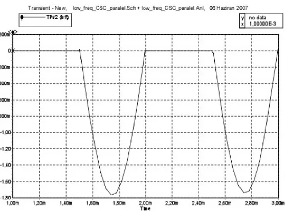
Figure 17a. Simulation result of CSC-parallel capacitor- for bipolar pacing mode
4.2 PART II: INDUCED VOLTAGE SIGNAL MODEL
In these simulations, it is assumed that proposed device that contains IPG and wires is placed in MRI scanner. 5 cm length of IPG width and 35 cm length of wire are placed in parallel to electric field of the MRI scanner. It is stated in the Halise’s Irak master thesis that 37.5 volt rms induced voltage on the electrode tissue impedance is calculated for 35 cm copper wire. This voltage value will be used as a signal source above simulations [26].
4.2.1 DIODE RESISTOR CIRCUIT (DRC)
In order to simulate this implementation, OrCAD PSpice 9.1 Demo (Cadence, 2655 Seely Avenue, San Jose, California 95134, USA) was used. In this simulation, Infineon Technologies BA595 pin diode model was used. 37.5 volt rms induced voltage at 64 MHz applied as a signal source. Resistance of the resistor was selected as 100 kΩ. Result of this simulation is given in Table 3.
As a result of this simulation, approximately 3.2 volt rms induced voltage was observed on the electrode (1 kΩ electrode tissue impedance). It is concluded that DRC decreases significantly voltage level at the electrode of the lead. Gradient field simulation was not performed because PIN diode cannot blocks low frequency current flow.
4.2.2 TRANSISTOR DIODE CIRCUIT (TDC)
In this simulation, 5Spice Electronic Circuit Simulation Program (Non-commercial Version, Richard P. Andresen, 2004) was used. 1N5711 Schottky Barrier Diode was used. Table 1 MOSFET Models were used for PMOS and NMOS transistor. 37.5 volt rms induced voltage at 64 MHz was applied as a signal source. As a result of this simulation, approximately 1 volt rms induced voltage was observed at the electrode impedance. 1 volt rms induced voltage was observed on the ring impedance. Significant voltage drop was
observed on the electrode tissue impedance in this simulation result. This result is seen in Table 3.
In addition to RF simulation, gradient field simulation was performed. In order to compare these results with RF induced voltage response of my designs, 37.5 volt rms induced voltage at 1 KHz applied as a signal source. The voltage was measured on electrode tissue impedance of the electrode and ring of the lead and the voltage value dropped significantly in this simulation. Its value was measured as 0.37 volt rms voltage and this result showed that this implementation block RF induced voltage effectively. This result is seen in Table 3.
4.2.3 CAPACITOR SWITCH CIRCUIT (CSC)
In the simulation of this implementation, 27 KΩ resistors are placed on the leads. 5Spice Electronic Circuit Simulation Program (Non-commercial Version, Richard P. Andresen, 2004) was used. 37.5 volt rms induced voltage at 64 MHz was applied as a signal source and CSC -parallel capacitance model- was simulated. As a result of this simulation, approximately 1.4 volt rms induced voltage was observed on the electrode tissue impedance and approximately 1.7 volt rms induced voltage was observed on the ring electrode tissue impedance. This result is seen in Table3.
Also gradient field simulation was performed. 37.5 volt rms induced voltage at 1 KHz applied as a signal source. Simulation result of induced voltages at the electrode tissue impedance and ring tissue impedance are seen in Figure 18a and 18b.
Figure 18a. Simulation result of CSC-parallel capacitor- on the electrode tissue impedance at 1 KHz
Figure 18b. Simulation result of CSC-parallel capacitor- on the ring tissue impedance at 1KHz
Induced voltage level and shape was different on the electrode and ring impedances. Reason of this situation is PMOS transistors’ placement on the electrode wire. In fact, still measured induced voltage levels significantly decrease on both electrode and ring tissue impedances. Same simulations were repeated for CSC-series capacitor- implementation at 64 MHz and 1 KHz frequency. This result is seen in Table 3.
Design Measured voltage on
electrode-ring tissue impedance (Vrms)
64 MHz 1 KHz
DRC 3.2 ---
TDC 1 0.37
CSC –Parallel Capacitor 1.4(electrode) 1.7(ring)
0.64(electrode) 2.1(ring)
CSC- Series Capacitor 1.56 1.3
Table 3. Simulation result of DRC, TDC and CSC voltage measurement on the electrode and ring impedances.
4.3 PART III: EFFICIENCY MODEL OF CSC
Efficiency equation of CSC was solved by using MATLAB (The MathWorks Inc., Natick, Massachusetts, USA) with respect to R1 and C values. In Figure 19, the efficiency is plotted
Figure 19. The efficiency plot of CSC as a function of R1
In Figure 20, the efficiency is plotted as a function of capacitance for R1=50 kΩ ,
t
1=1 sec ,Figure 20. The efficiency plot of CSC as a function of capacitance
According to this solution, capacitance was selected as C= 10 µF and resistance of a resistor was selected as 50 kΩ. The efficiency was greater than 15 (η>=15) for these values. In order to block passage of RF current from gate of MOSFET to electrode and ring, 100 kΩ resistor is put on the control line of MOSFET transistor gate for both implementations. This resistor does not affect pulse process because there is no current on the MOSFET transistor gate. Thus, DC voltage level on the control line is not changed by putting this resistor.
In Figure 21, the efficiency is plotted as a function of
t
1 for C= 10 µF, R1=50 kΩ,t
2=1Figure 21. The efficiency plot of CSC as a function of t1
In Figure 22, the efficiency is plotted as a function of
t
2 for C= 10 µF, R1=50 kΩ,t
1=1 sec,R2=1 kΩ .
These plots give idea about effect of charging and discharging duration on the efficiency of the system.
According to above calculations, specific resistance and capacitance values are determined. In this design, modification is available when resistance distribute on the wire. Resistance of wire can be calculated as:
R
L
A
ρ
=
(6)where
ρ
is resistivity, L is length, A is the cross sectional area of the wire.Based on the calculation above, the optimum resistance which is placed on the electrode wire is calculated as 25 kΩ . The same resistance is also placed on the ring wire. If it is assumed that length of the wire is 50 cm and copper is used as a material. Resistivity of copper is
ρ=1.724x10
-8Ωm
at 20 C. By using this data, diameter of the copper wire is calculated asd=6.63x10
-4mm
In addition to this, if another element is used, for example carbon (
ρ=3.5x10
-5Ωm
), the new diameter of the wire will bed=2.986x10
-2mm
. These two calculations show that a very thin wire can be used and also different materials, which are highly resistive, can be used in this design.5. EXPERIMENTS
In this chapter, the experimental methods used to observe performance of the proposed designs are explained. Phantom heating experiments of wire with and without RF blocking elements for DRC and CSC are performed. The nerve stimulation experiment of CSC is also performed in the following part. The experimental method is described below.
5.1 HEATING MEASUREMENT EXPERIMENTS
In the first section, heating experiment setups of wire with and without RF blocking elements are explained. In the second and third sections, heating experiment setups of DRC and CSC are explained.
5.1.1 COMPARISON OF WIRE HEATING WITH AND WITHOUT RF
BLOCKING ELEMENTS (RFBE)
Experiment was performed to observe heating response of wire with and without RF blocking elements. In this experiment, Fast SPGR sequence was used with following imaging parameters: Body coil (diameter: 60 cm), matrix 256x256, NEX: 4, TE: min, TR: 19 msec, flip angle: 90, bandwidth: 62.5 KHz, FOV: 48, Slice thickness: 20 mm.
The Scanner software estimated the average SAR as 1.26 W/Kg, and peak SAR as 2.51 W/Kg. It should be noted that, while scanner estimates these numbers, it assumes that a person as weighs 30 Kg., and therefore, the estimation method used in the scanner may fail to display the correct number.
A semi cylindrical phantom (19.5 cm diameter, 50 cm length, and see Figure 23) was constructed that enabled accurate and reproducible placement of wire and temperature measuring probes in a gel to measure temperature increase.
Figure 23. Semi cylindrical phantom model.
The phantom consisted of a gel. This gel consisted of 4 lt. water, 1.6 kg gel flour and 50 gr. salt without iodine.
Copper hookup wire with 0.5 mm diameter was straightened and cut into 30 cm lengths. Three cases were tested: wire without any RF blocking element on it, wire with 3.9 kΩ resistor placed on the distal electrode of the wire and wire with PIN diode MA4P7452F-1072T (M/A-COM, Pawtucket Blvd., Lowell, USA) placed on the distal electrode of the wire.
The gel phantom was placed longitudinally in the scanner, with the wire placed longitudinally in it. In order to obtain high electrical field strength in the gel phantom, it was placed within 0 to 1 cm away from main body coil of the scanner. In addition to this, the lead was placed within 3 to 5 cm away from phantom edge that is close to body coil of the scanner. According to this adjustment, bare sides of lead were placed inside the gel, and remaining part was placed on the surface of the gel.
Figure 34. Lead placement in the gel
Figure 26. Lead model without RFBE used in the heating measurement
Figure 27. Lead model with RFBE used in the heating measurement
5.1.2 DIODE RESISTOR CIRCUIT (DRC)
Experiment was performed to observe heating response of DRC. In this experiment, Fast SPGR sequence was used with following imaging parameters: Body coil (diameter: 60 cm), matrix 256x256, NEX: 4, TE: min, TR: 19 msec, flip angle: 90, bandwidth: 62.5 KHz, FOV: 48, Slice thickness: 20 mm.
The Scanner software estimated the average SAR as 1.26 W/Kg, and peak SAR as 2.51 W/Kg. The phantom is semi cylinder with a 10 cm radius and a 50 cm length. This gel phantom setup is seen in Figure 28a and 28b.
Figure 28a. Gel phantom setup with DRC
5.1.3 CAPACITOR SWITCH CIRCUIT (CSC)
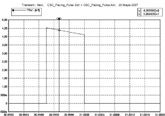
With the aim of testing the CSC- parallel capacitor- circuit, a circuit that emulates implantable pace generator (IPG) was designed. The simple pulse circuit contained a standard 9 Volt battery, and a 16F84A 18-pin Enhanced FLASH/EEPROM 8-Bit microcontroller. 16F84A microcontroller was programmed to generate 1msec pulse with a period of 1 sec. 9 Volt battery and 16f84A microcontroller were put on the same board and connected to each other. This board was put into a waterproof plastic box with the dimension of 9.5x5x2.5 (cm). Approximately 29 cm copper wires (0.5 mm diameter) were connected to this box .The waterproof plastic box was covered with copper tape and this conductive coating was connected to ground wire.
Different than IPG box of this design, another mini box design was made in order to place CSC on the lead of the IPG. In this mini box, 27 kΩ resistor was used. 500 kΩ resistor connected to gate of PMOS transistor due to obtain reliable gate isolation for RF signal during MRI examination. 10 µF tantalum capacitor and BS250 PMOS transistor were placed in the circuit. CSC (parallel capacitor) was built by using these components.
After mini box that contain CSC was added at the end of the lead, total length of wire was approximately 35 cm and my safe implantable circuit design was created simply. In order to compare the safety performance of CSC implementation, an IPG model without CSC circuit was created. Two designs are seen in Figure 29a and Figure 29b.
Figure 29a. IPG model without CSC
Figure 29b. IPG model with CSC
These two circuits were put into approximate rectangular plastic phantom which dimension is 51x14.7x11 (cm) (Figure 30a and 30b).
Figure 30a. Rectangular plastic phantom side 1