Electrochemical Atom-by-Atom Growth of PbS by Modified ECALE Method
Tuba O¨ znu¨lu¨er, I˙brahim Erdogˇan, I˙lkay S¸is¸man, and U¨ mit Demir*
Department of Chemistry, Arts and Sciences Faculty, Atatu¨rk UniVersity, 25240, Erzurum-Turkey ReceiVed October 7, 2004 ReVised Manuscript ReceiVed January 22, 2005
The electrochemical growth of single-crystal thin films of II-VI compound semiconductors, such as CdS,1ZnS,2and PbS,3 on foreign single crystal substrates has received considerable attention for use in photovoltaic and light-emitting devices, as well as in numerous optoelectronic applications. Since the properties of semiconductors depend on both dimension and superlattice structure, the film must be highly crystalline and have a particular single crystal-lographic orientation. Electrochemical atomic layer epitaxy (ECALE), developed by Stickney,4has been used to produce a wide variety of well-ordered semiconductor deposits. The principle of ECALE is that a deposit is formed one atomic layer at a time, using surface limited reactions through underpotential deposition (upd),5 in a repeating cycle. Separate solutions and potentials are used to deposit atomic layers of each element electrochemically in a cycle in this method. The problems with this technique are that the electrode is required to be rinsed after each upd deposition, which may result in loss of potential control, deposit reproducibility problems, and waste of time and solution. Automated deposition systems for ECALE were developed to overcome these problems.6Another particularly promising method is successive ionic layer adsorption and reaction (SILAR) which is based on the sequential immersing of the substrates in solutions of each element, with rinsing between with water.7PbS has been prepared by cycling the potential between anodic and cathodic potentials using the disodium salt of ethylenediaminetetraacetic acid (EDTA) as a com-lexing agent for Pb.8Here, we report a new electrochemical process based on the co-deposition of Pb and S precursors from the same solution containing EDTA, Pb2+, and S2-at a constant potential, which is determined from the upd potentials of Pb and S. Preliminary results indicate that this one-step process could also be used for the electrochemical
deposition of II-VI compound semiconductors in the form of single crystalline thin film. Additionally, this method allows easy control of the thickness of the material by simply using different deposition times and has some advantages over the present electrochemical deposition methods to overcome the deposition problems mentioned above.
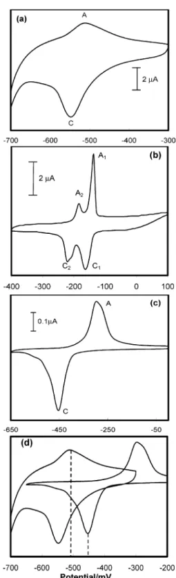
Figure 1a shows a typical cyclic voltammogram of 0.001 M Na2S in the range of S upd containing 0.1 M EDTA at Au(111) electrode. The voltammetric behavior of S upd is essentially identical to that reported previously.9,10The broad anodic deposition peak (A, around -520 mV) is associated with the broad stripping peak (C, around -570 mV) of one atomic layer of S. The underpotential deposition of Pb was performed on the Au(111) in the solution containing 0.05 M Pb2+ ions with and without 0.1 M EDTA. The voltam-mograms for Pb upd from aqueous solution, without EDTA, are quite similar to those reported in the literature at the same pH (Figure 1b).11In the presence of EDTA, as a complexing agent for Pb2+, the cyclic voltammogram of Pb on the Au-(111) surface contains only one redox couple corresponding to deposition and stripping of Pb atomic layers and ∆Ep (difference between cathodic and anodic peak potentials) is quite different from those obtained on Au(111) electrodes in aqueous solution. The cathodic deposition wave was shifted negatively, so that ∆Epwas more than 160 mV. A similar shift has been observed for the deposition of Pb on an Au(111) electrode coated with a self-assembled monolayer (SAM) of alkanethiols due to blocking effect of SAM.12 Charge integration of stripping peak A yields values of 255(5µC/cm2, which corresponds to the values reported for one atomic layer of Pb in the literature,13assuming 2 e-/Pb adatom. The charge corresponding to the stripping of Pb was constant for different deposition times at constant potential and the peak current was independent of the Pb2+ concentration. Therefore, these peaks are considered to result from Pb upd. When we added S2-, Pb2+, and EDTA to a single solution, no precipitation was observed.
The cyclic voltammograms of S upd and Pb upd in EDTA solutions are also shown in figure (Figure 1d). If the potential of the electrode was kept constant at a potential in the middle of both upd waves of Pb and S, Pb and S were deposited simultaneously at the electrode. Since the value of this potential is not enough for the bulk deposition of either Pb or S, there was no deposition of Pb2+on Pb or S2-on S. In other words, the potential between the dotted lines shown in Figure 1d is limited for the upd deposition of both Pb and S atomic layers but not for bulk deposition. Therefore, it should promote atom-by-atom growth of PbS at the substrate, while keeping Pb complexed, avoiding the forma-tion of PbS particles in the soluforma-tion phase so they do not * To whom correspondence should be addressed. Tel: +90-442-2314434.
Fax: +90-442-236 0948. E-mail: [email protected]. (1) Demir, U¨ .; Shannon, C. Langmuir 1994, 10, 2794.
(2) Gichuhi, A.; Boone, B. E.; Demir, U¨ .; Shannon, C. J. Phys. Chem. B 1998, 102, 6499.
(3) Torimoto, T.; Takabayashi, S.; Mori, H.; Kuwabata, S. J. Electroanal. Chem. 2002, 522, 33.
(4) Gregory, B. W.; Stickney, J. L. J. Electroanal. Chem. 1991, 300, 543. (5) Kolb, D. M. In AdVances in Electrochemistry and Electrochemical Engineering; Gerischer, H., Tobias, C. W., Eds.; Wiley Interscience: New York, 1978; Vol. 11, p 125.
(6) Flowers, B. H., Jr.; Wade, J.; Garvey, W.; Lay, M.; Happek, U.; Stickney, J. L. J. Electroanal. Chem. 2002, 524-525, 273. (7) Nicolau, Y. F. Appl. Surf. Sci. 1985, 22, 1061.
(8) Saloniemi, H.; Ritala, M.; Leskale, M.; Lappalainen, R. J. Electrochem. Soc. 1999, 146 (7), 2522.
(9) Alanyalioglu, M.; Cakal, H.; O¨ ztu¨rk, A. E.; Demir, U¨. J. Phys. Chem. B 2001, 105, 10588.
(10) Gao, X.; Zhang, Y.; Weaver, M. J. J. Phys. Chem. 1992, 96, 4156. (11) Alvarez-Rizatti, M.; Juttner, K. J. Electroanal. Chem. 1983, 144, 351. (12) Oyamatsu, D.; Kuwabata, S.; Yoneyama, H. J. Electroanal. Chem.
1999, 473, 59.
(13) Hamelin, A. J. Electroanal. Chem. 1979, 101, 285.
935 Chem. Mater. 2005, 17, 935-937
10.1021/cm048246g CCC: $30.25 © 2005 American Chemical Society Published on Web 02/05/2005
contribute to film growth. On the basis of this idea, we have attempted to use this method to synthesis PbS thin films with various thicknesses by simply using different deposition times from the same solution.
Figure 2 shows an AFM image of PbS deposited at -480 mV for 30 min in the solution containing 0.001 M Na2S, 0.05 M Pb(CH3COO)2, and 0.1 M EDTA on the Au(111) single crystalline electrode. The surface of the PbS consists of square terraces, which are characteristic of (200) single
crystal with a cubic structure. The square features intercept each other at essentially 45°, and this is consistent with the in-plane orientation of the film. These square crystals were as large as 1000 nm, unreachable by any of the previously studied electrochemical methods. This means that the present technique results in long-range atom-by-atom growth of PbS, yielding a film composed of highly crystallized PbS.
The X-ray diffractogram of the PbS is shown in Figure 3, where the diffraction peak was assigned as PbS (200). These XRD data indicate that the PbS crystals have a diffraction pattern corresponding to the cubic structure. It is supposed that the growth of PbS thin films follows (111) orientation since the films are grown on the Au(111) substrate. Switzer et al. have previously shown that electrodeposited epitaxial films of Cu2O follow a transition from a thermodynamically controlled orientation to a kinetically preferred orientation on Au(111) at pH 9 after a critical thickness.14AFM images obtained on Au (111) exhibited the same cubic structure of PbS and the reflections of PbS gave full width at
half-Figure 1. Cyclic voltammogram of Au electrode in the solution containing
(a) 0.001 M Na2S and 0.1 M EDTA; (b) 0.05 M Pb(CH3COO)2; (c) 0.05
M Pb(CH3COO)2and 0.1 M EDTA; and (d) overlapped voltammograms
shown in (a) and (c) at 100 mV/s.
Figure 2. AFM images of PbS formed on the Au(111) electrode after potential controlled deposition at -480 mV for 30 min.
Figure 3. XRD patterns of the PbS sample electrodeposited onto
single-crystal Au(111) in Figure 2.
maximum (fwhm) values of 0.25°. These results indicate that highly crystalline deposits of PbS can be grown at kinetically preferred orientation on Au (111). The Pb/S ratios of electrodeposits were determined with EDS analysis, close to the stoichiometric value of 1.
Studies of the detailed mechanism of the electrochemical formation of II-VI films on Au(111) are currently in progress. We are currently extending the protocols described herein to prepare II-VI compound semiconducting materials. To use this method, both precursors of the II-VI compounds have to have upd behavior and their upd waves should not overlap within the bulk deposition potential range for the
other element. Our preliminary results indicate that it is possible to form highly crystalline deposits of ZnS, ZnTe, CdS, and CdTe by this method and will be reported in the near future. In conclusion, we have shown that it is possible to grow highly crystalline deposits of PbS by a novel electrochemical method, which is based on a simple idea, in which Pb is complexed to prohibit the precipitation in the solution. Then, both of the Pb and S precursors are deposited from the same solution at a constant potential at which both upd waves occur.
Supporting Information Available: Experimental section, including electrochemistry and instrumentation (pdf). This material is available free of charge via the Internet at http://pubs.acs.org. CM048246G
(14) Switzer, J. A.; Kothari, H. M.; Bohannan, E. W. J. Phys. Chem. B 2002, 106, 4027.