Complementary Spiral Resonators for Ultrawideband Suppression of
Simultaneous Switching Noise in High-Speed Circuits
Amir Ghobadi1, 3, *, Kagan Topalli2, Necmi Biyikli3, 4, and Ali Kemal Okyay1, 3, 4
Abstract—In this paper, a novel concept for ultra-wideband simultaneous switching noise (SSN) mitigation in high-speed printed circuit boards (PCBs) is proposed. Using complementary spiral resonators (CSRs) etched on only a single layer of the power plane and cascaded co-centrically around the noise port, ultra-wideband SSN suppression by 30 dB is achieved in a frequency span ranging from 340 MHz to beyond 10 GHz. By placing a slit in the co-centric rings, lower cut-off frequency is reduced to 150 MHz, keeping the rest of the structure unaltered. Finally, the power plane structure with modified complementary spiral resonators (MCSRs) is designed, fabricated, and evaluated experimentally. Measurement and simulation results are in well-agreement.
1. INTRODUCTION
With the ever increasing demand for modern high-speed digital circuits with high clock frequencies, fast edge rates and low voltage consumption, simultaneous switching noise (SSN) also known as ground bounce noise (GBN) has received considerable attention in the past few years. In modern high-speed printed circuit boards (PCBs), propagation of parallel plate waveguide (PPW) resonance modes between power and ground planes excited by the SSN leads to a degradation in signal/power integrity (SI/PI) [1– 5]. In addition to this degradation, SSN can cause various low and high frequency anomalies that can lead to false switching and logic errors in digital circuits [6]. By taking all into consideration, mitigation of this noise becomes a critical necessity in today’s high speed circuits.
Different approaches have been investigated to mitigate SSN. Adding discrete and embedded decoupling capacitors has been the most frequently used method proposed to mitigate SSN [7–9]. This conventional technique, however, has some practical limitations. Owing to dominant inductive behavior at higher operational frequencies, this technique does not provide sufficient mitigation beyond 500 MHz [10]. In recent years, electromagnetic band gap (EBG) [11–13] and high impedance surface (HIS) [14–16] structures have been proven as promising solutions for suppression of noise in the gigahertz frequency range. Typically, an additional metal layer is required to implement EBG and HIS structures. Also in embedded configurations, metal-via structures are required which are usually undesired in manufacturing process. EBG and HIS structures suffer from (i) increased manufacturing complexity and therefore high cost, and (ii) typical operation bandwidth of these structures covers a narrow frequency range. In order to build a stable power distribution network in high-speed digital circuits, SSN should be suppressed properly in the entire frequency range of operation from couple of hundred megahertz up to several gigahertz. To cope with these stringent requirements, complementary split ring resonator (CSRR) was introduced [17]. In addition to having a planar structure with no additional metal layers or vias, this structure can mitigate noise propagation in an ultra-wideband frequency range. The design in [17] was able to suppress noise propagation by 20 dB for frequencies higher than 1 GHz (1–12 GHz band). In order to lower the cut-off frequency to below 1 GHz, physical dimensions need to be scaled up,
Received 2 December 2013, Accepted 5 January 2014, Scheduled 9 January 2014
* Corresponding author: Amir Ghobadi ([email protected]).
1 Department of Electrical and Electronics Engineering, Bilkent University, Ankara 06800, Turkey. 2 Department of Electrical and Electronics Engineering, TED University, Ankara 06420, Turkey. 3 UNAM-National Nanotechnology Research Center, Bilkent University, Ankara 06800, Turkey.4 Institute of Materials Science and Nanotechnology, Bilkent University, Ankara 06800, Turkey.
which quickly becomes prohibitively large. Alternatively, additional components (decoupling capacitors) could be used, which makes integration more complex.
In this paper, we propose planar complementary spiral resonators (CSRs) to suppress SSN in an ultra-wideband frequency range starting from 340 MHz up to 10 GHz and beyond. Furthermore, by placing a slit in the co-centric rings, we show that the lower cut-off frequency can be reduced to 150 MHz which is almost 10 times smaller than previous work without any dimensional scaling. In the following sections, we provide some details about electromagnetic behavior and working principle of CSR structures and its contribution in our proposed power plane.
2. NOISE MITIGATION USING CONCENTRICALLY CASCADED CSRS
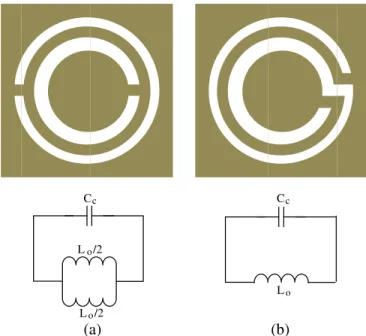
The CSR is an electrically small resonant structure with a slot etched in a metallic layer which is shown in Fig. 1. The electromagnetic behavior of CSR is complementary to SR. As it is explained in [18] SR structures act like an LC resonator providing an effective propagation bandgap for a time varying magnetic field with a polarization perpendicular to the surface of the loop, however CSR exhibits this characteristic for an electric field polarized normal to the loop surface. As shown in Fig. 2, equivalent circuit for both structures can be viewed as a simple parallel LC resonator. In both structures, the capacitance Cc is the capacitance of a disk with radius of ro−a2 (where ro is average radius and a is
slot width) surrounded by a metallic plane.
H K E H K b a a r (a) (b)
Figure 1. Schematic of (a) spiral resonator (SR) and (b) complementary spiral resonator (CSR). For CSRR, the inductance Lo, which results from the current path through the rings, is a parallel
combination of the two inductances modeling current flow from inner disk to the ground, as reported in [19]. However, in the CSR, inductance is comprised of the inductance of inner metal ring around the whole circumference. Therefore, amount of total equivalent inductance is four times larger for CSR compared to CSRR. Therefore the resonance frequency of CSR design is half of that of CSRR with identical radius and dimensions. In other words, electrical length (diameter) of CSR is one half that of CSRR (for the same physical scale) so it can lead to size reduction of two-fold for our design. It should be noted that an analytical approximate expression for capacitance of Cc values for both designs are
provided by authors in [19], whereas Lo is equivalent to inductance of a circular co-planar-waveguide
(CPW) with strip width of b, slot width of a and external radius of ro and a numerical expression for
Lo can be found at [20].
Owing to the fact that a CSR structure etched on a single metallic layer exhibits negative effective permittivity in the vicinity of its resonance frequency and acts like a narrow band-stop filter for propagation of waves through the continuous transmission line [21], it is expected that, if several CSRs with different radii resonating in different frequencies are co-centrically cascaded, an ultra-wideband noise suppression can be achieved and the overall effect would be an ultra-wideband filter with a stop-band characteristic equivalent to superposition of the original individual filters. In the following sections, we demonstrate mitigation capability of co-centrically cascaded CSRs.
C Lo Lo Cc /2 /2 Lo Cc (a) (b)
Figure 2. Topology and circuit model of (a) complementary split ring resonator (CSRR) and (b) complementary spiral resonator (CSR).
Port1 Port2
r Ground Plane
Microstrip Line
Figure 3. Simulation model used to identify the resonance frequencies of the CSR. 3. RESULTS AND DISCURSION
High frequency structural simulator (HFSS) was used to simulate CSR structures with different radii to get an estimate about their resonance frequencies. For this aim, a simple micro-strip transmission line structure is used as it is mentioned in [22] and is shown in Fig. 3. It should be emphasized that this structure is not identical to our power plane design but can provide a rough estimation about radii for the final design. The substrate employed for this micro-strip line is the commercially available PCB made of FR4 dielectric with a thickness of 1.54 mm and dielectric constant of ²r = 4.4. CSRs with
different radii are etched in ground plane underneath the conductor strip with a width of 3 mm. Fig. 4 plots measured transmission coefficient (S21) values for different radii. The values of these radii have
been chosen in a way that a superposition of S21values for cascaded CSR structure could cover a whole
frequency range starting from couple of hundred megahertz up to several gigahertz.
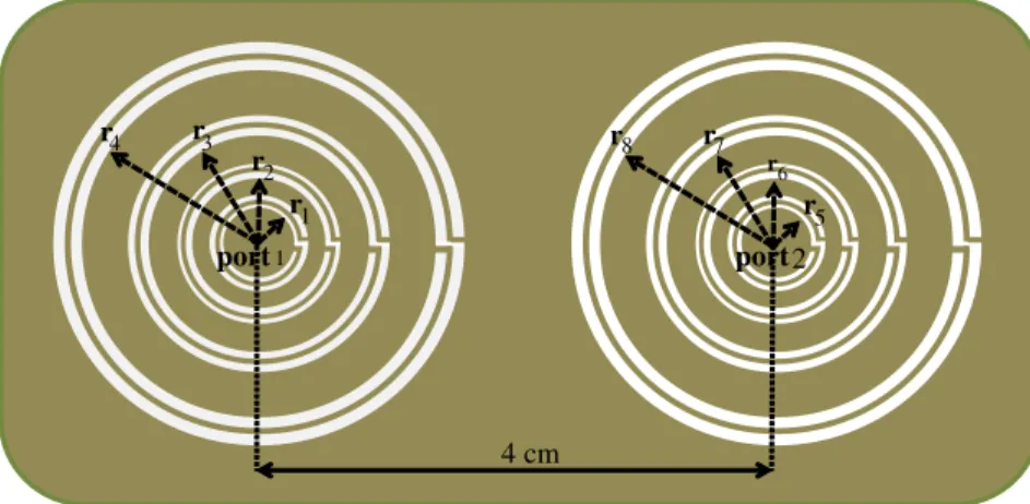
Using initial values for radii, noise mitigation capability of centrally cascaded CSRs are investigated by carrying out simulations for power plane structure based on setup provided in Fig. 5. In this design, Port-1, source of switching noise, is surrounded with four CSRs with different radii. At the opposite side, electromagnetic wave propagating through waveguide will be collected with output port (Port-2) placed 4 cm away from Port-1 and encompassed with another set-of-four co-centrically placed CSRs to provide further mitigation in incoming noise. The noise suppression property of proposed power plane can be confirmed using the results of insertion loss (S21) between two ports in the frequency domain.
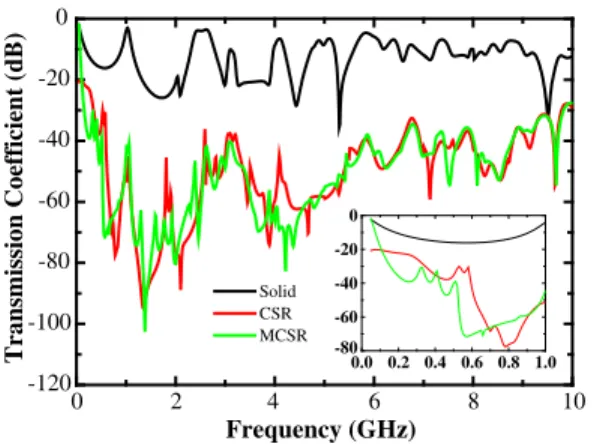
Fig. 6 shows the simulated results for the proposed CSR design, in comparison with a solid bare board as a reference. These results are achieved by simulation based fine-tuning for set of co-centrically placed
0 2 4 6 8 10 -16 -14 -12 -10 -8 -6 -4 -2 0 Transmission Coefficient (dB) Frequency (GHz) r = 6.8mm r = 7.5mm r = 9.2mm r = 11mm
Figure 4. Transmission coefficient results for different radii of CSR.
1 2 3 4 5 8 7 6 1 2 4 cm r r r r r r r r port port
Figure 5. Schematic representation of proposed power plane with CSRs etched on it.
CSRs with different radii of r1 = 7.5, r2 = 8.2, r3 = 10.3, r4= 11, r5= 7.4, r6 = 8.4, r7= 9.2, r8 = 10.4
as shown in Fig. 5 and because of fabrication considerations (minimum resolution of isolation lines by our PCB plotter), the width of slots and strips (a and b) are kept as 0.2 mm. In this paper, bandwidth is defined as the frequency span where S21is lower than −30 dB. According to this definition, the power
plane with co-centrically cascaded CSRs can show suppression bandwidth from 340 MHz to 10 GHz. Also it should be noted that this design has been made on FR4 substrate with thickness of 1.54 mm and overall size of 60 mm × 70 mm.
In order to expand the operational bandwidth to lower cut-off frequencies, the above design is improved to a modified CSR (MCSR) structure. As it can be seen from Fig. 7, there are three paths (in the second ring) over which current can flow. These currents are named I1, I2, and I3. Due to direction
of these currents, in some parts of the structure destructive coupling occurs which in turn decreases the total inductance. In the other words, opposite-directed current distribution in two adjacent turn leads to small effective inductance and as a result, the resonance frequency is high.
From Fig. 7(a), we observe that the current I2 is passing in the opposite direction in comparison
with I and I3. Therefore, it has destructive coupling with these two current distributions and makes
total inductance smaller. In order to eliminate the effect of this destructive coupling, the CSR structure was modified and a cut, in the shape of a slit, is made in the outer ring as shown in Fig. 7(b). This way, the main cause of destructive coupling, I2, is eliminated and the overall effective inductance is increased.
This, in turn, shifts resonance to lower frequencies. As it can be seen from Fig. 8, by proposing this simple modification, the lowest frequency edge where S21 is lower than −30 dB is almost halved down
0 2 4 6 8 10 -120 -100 -80 -60 -40 -20 0 Solid CSR Transmission Coefficient (dB) Frequency (GHz)
Figure 6. Simulated transmission coefficient results for solid (without CSR) and power plane with CSRs etched on it. I 2 3 1 I I I I I 2 3 (a) (b) I
Figure 7. (a) The paths for current in cascaded CSR and (b) modified CSR structure.
0 2 4 6 8 10 -120 -100 -80 -60 -40 -20 0 Solid CSR MCSR Transmission Coefficient (dB) Frequency (GHz) 0.0 0.2 0.4 0.6 0.8 1.0 -80 -60 -40 -20 0
Figure 8. Simulated transmission coefficient results in comparison with power plane having CSRs and MCSRs etched on it.
to 150 MHz while keeping all the dimensions unchanged.
To verify validity of simulation results, the power plane structure with radii obtained from simulation is fabricated. Fig. 9 shows fabricated prototype of proposed design. Fabrication of proposed power plane structure was done by LPKF ProtoMat° S62 PCB plotter. The measurements are carriedR
out using a network analyzer (Agilent E5071C). According to Fig. 10, there is an excellent agreement between simulation and measurement results especially in lower frequencies. Because of dispersion property of the FR4 substrate and the conduction losses which are not considered in the simulation, a slight deviation between simulation and measurement results is seen at higher frequencies.
(a) (b)
Figure 9. (a) Front and (b) back view of fabricated prototype of proposed power plane with MCSRs etched on it. 0 2 4 6 8 10 -100 -80 -60 -40 -20 0 Transmission Coefficient (dB) Frequency (GHz) Simulation Measurement 0.0 0.2 0.4 0.6 0.8 1.0 -75 -50 -25 0
Figure 10. Simulation and measurement results for fabricated design. 4. CONCLUSIONS
We have demonstrated an ultra-wideband suppression method of simultaneous switching noise in high-speed circuits using concentrically cascaded CSRs. Besides having ultra-wideband mitigation this design can be fabricated easily in comparison with previous techniques that suffer from manufacturing complexity and cost perspectives. It is shown that by using this configuration a broad operation frequency range between 340 MHz and 10 GHz is covered for −30 dB suppression bandwidth. By reducing destructive inductive contribution using a slit in the co-centric rings, lower cut-off frequency is extended to 150 MHz without any scaling in dimensions or sacrificing the performance elsewhere. ACKNOWLEDGMENT
This work was supported by the Scientific and Technological Research Council of Turkey (TUBITAK),grant numbers 109E044, 112M004, 112E052, 113E126 and 113M815, European Union FP7 Marie Curie IRG grants 239444 and 249196. N. B. acknowledges support from Marie Curie International Reintegration Grant (NEMSmart, Grant # PIRG05-GA-2009-249196). A. K. O. acknowledges a Marie Curie International Reintegration Grant (PIOS, Grant # PIRG-GA-2008-239444).
REFERENCES
1. Ren, K., C. Y. Wu, and L. C. Zhang, “The restriction on delta-I noise along the power/ground layer in the high speed digital printed circuit board,” Proc. IEEE Int. Electromagn. Compat. Symp., 511–516, Denver, CO, Aug. 1998.
2. Kamgaing, T. and O. M. Ramahi, “A novel power plane with integrated simultaneous switching noise mitigation capability using high impedance surface,” IEEE Microw., Wireless Component
Lett., Vol. 13, No. 1, 21–23, 2003.
3. Wu, T. L., S. T. Chen, J. N. Hwang, and Y. H. Lin, “Numerical and experimental investigation of radiation caused by the switching noise on the partitioned DC reference planes of high speed digital PCB,” IEEE Trans. on Electromagn. Compat., Vol. 46, No. 1, 33–45, 2004.
4. Swaminathan, M., “Power distribution networks for system-on-package: Status and challenges,”
IEEE Trans. on Advanced Packaging, Vol. 27, No. 2, 286–230, 2004.
5. Lei, G. T., R. W. Techentin, and B. K. Gilbert, “High frequency characterization of power/ground-plane structures,” IEEE Trans. on Microwave Theory and Techniques, Vol. 47, No. 5, 562–569, 1999.
6. Ramahi, O., V. Subramanian, and B. Archambeault, “A simple finite difference frequency-domain (FDFD) algorithm for analysis of switching noise in printed circuit boards and packages,” IEEE
Trans. on Advanced Packaging, Vol. 26, No. 2, 191–198, 2003.
7. Archambeault, B., “Analyzing power/ground plane decoupling performance using the partial element equivalent circuit (PEEC) simulation technique,” IEEE Int. Electromagn. Compat. Symp., 779–784, Washington, DC, Aug. 2000.
8. Archambeault, B. and A. E. Ruehli, “Analysis of power/ground plane EMI decoupling performance using the partial-element equivalent circuit technique,” IEEE Trans. on Electromagn. Compat., Vol. 43, No. 4, 437–445, 2001.
9. Madou, A. and L. Martens, “Electrical behavior of decoupling capacitors embedded in multilayered PCBs,” IEEE Trans. on Electromagn. Compat., Vol. 43, No. 4, 549–556, 2001.
10. Xu, M., T. H. Hubing, J. Chen, T. P. Van Doren, J. L. Drewniak, and R. E. DuBroff, “Power-bus decoupling with embedded capacitance in printed circuit board design,” IEEE Trans. on
Electromagn. Compat., Vol. 45, No. 1, 22–30, 2003.
11. Shahparnia, S. and O. Ramahi, “Miniaturised electromagnetic bandgap structures for broadband switching noise suppression in PCBs,” Electron. Lett., Vol. 41, No. 9, 519–520, 2005.
12. Kwon, J. H. and J. G. Yook, “Partial placement of EBG on both power and ground planes for broadband suppression of simultaneous switching noise,” IEICE Trans. on Commun., Vol. E92-B, No. 7, 2550–2553, 2009.
13. Shahparnia, S. and O. Ramahi, “Electromagnetic interference (EMI) reduction from printed circuit boards (PCB) using electromagnetic bandgap structures,” IEEE Trans. on Electromagn. Compat., Vol. 46, No. 4, 580–587, 2004.
14. Kamgaing, T. and O. Ramahi, “A novel power plane with integrated simultaneous switching noise mitigation capability using high impedance surface,” IEEE Microw. Wirel. Compon. Lett., Vol. 13, No. 1, 21–23, 2003
15. Chang, C. S., M. P. Houng, D. B. Lin, K. C. Hung, and I. T. Tang, “Simultaneous switching noise mitigation capability with low parasitic effect using aperiodic high-impedance surface structure,”
Progress In Electromagnetics Research Letters, Vol. 4, 149–158, 2008.
16. Chang, C. S., J. Y. Li, W. J. Lin, M. P. Houng, L. S. Chen, and D. B. Lin, “Controlling the frequency of simultaneous switching noise suppression by using embedded dielectric resonators in high-impedance surface structure,” Progress In Electromagnetics Research Letters, Vol. 11, 149–158, 2009.
17. Bait-suwailam, M. M. and O. M. Ramahi, “Simultaneous switching noise mitigation in high-speed circuits using complementary split ring resonators,” IET Electron. Lett., Vol. 46, 563–564, 2010. 18. Baena, J. D., R. Marqu´es, F. Medina, and J. Martel, “Artificial magnetic metamaterial design by
using spiral resonators,” Phys. Rev. B, Condens. Matter, Vol. 69, 14402, 2004.
19. Baena, J. D., J. Bonache, F. Mart´ın, R. Marqu´es, F. Falcone, T. Lopetegi, M. A. G. Laso, J. Garc´ıa, I. Gil, and M. Sorolla, “Equivalent circuit models for split ring resonators and complementary split ring resonators coupled to planar transmission lines,” IEEE Trans. on Microw. Theory and Tech., Vol. 53, No. 4, 1451–1461, 2005.
20. Marqu´es, R., F. Mesa, J. Martel, and F. Medina, “Comparative analysis of edge- and roadside-coupled split ring resonators for metamaterial design. Theory and experiments,” IEEE Trans. on
Antennas and Propagat., Vol. 51, No. 1, 2572–2581, 2003.
21. Isik, O. and K. P. Esselle, “Backward wave microstrip lines with complementary spiral resonators,”
IEEE Trans. on Antennas and Propagat., Vol. 56, No. 10, 2008.
22. Falcone, F. T. Lopetegi, J. Baena, R. Marques, F. Martin, and M. Sorolla, “Effective negative stopband microstrip lines based on complementary split ring resonators,” IEEE Microw. Wireless