VOLUME 58, NUMBER 19
PHYSICAL REVIEW
LETTERS
11MAY 1987Metallization
of
Silicon
uponPotassium
Adsorption
S.
Ciraci'
and InderP.
BatraIBMZurich Research Laboratory, 8803Ruschlikon, Switzerland
(Received 24September 1986)
We report novel features ofpotassium deposition on a
Si(111)-(2x
1)surface as a function of cover-age. The binding is ionic even at the saturation coverage without any overlayer metallization. Up to athreshold coverage, the alkali-metal electrons are donated to the empty surface state resulting in a lD
metallic chain. Above this coverage, the conduction-band states are occupied, so that the surface
elec-trons become itinerant leading to the metallization ofthe substrate and onset ofenhanced conductivity.
PACSnumbers: 71.30.+h, 71.45.Gm, 73.40.Ns
Generation of desired electronic properties by metal deposition on the semiconductor surfaces has been ex-ploited in a number of technical applications in the area ofmicroelectronics. It is also now quite evident that one might expect interesting coverage-dependent effects, and,
in particular, the overlayer metallization may set in at a critical threshold. For those semiconductors which have active surface states, the metallization of the overlayer must compete with the formation of metal-semicon-ductor bonds. In fact, depending on the relative value of the metallic cohesive energy and the metal-substrate in-teraction energy the overlayer metallization may be suppressed altogether.
In this Letter, we report novel features of
Si(111)-(2X
I)
substrate metallization upon deposition of potas-sium as a function of coverage, Our calculations show that, up to a threshold coverage, the alkali-metal elec-trons are donated to the emptyz*
band' resulting in a 1D metallic system. Above this coverage, the Fermi lev-el crosses the bulk conduction-band minimum, so that the surface electrons become itinerant leading to the metallization of the substrate. An important aspect of this prediction is that the excess carrier concentration inthe conduction band can be controlled at will by K depo-sition. The critical adsorption coverage gives rise to the same physical eAects as bulk doping would, but without the introduction of any scattering centers in the bulk (and hence high mobility may be expected). We also show that the z-bonded chain structure' is stable under K adsorption. These conclusions are derived from total-energy minimization, force, and electronic-structure cal-culations on the monolayer, multilayer, and bulk potassi-um, as well as the clean and K-covered Sisurfaces.
Three key ingredients responsible for the unusual in-teraction between K and the
Si(111)
surface are(i)
a saturation coverage above the monolayer, (ii) ionic bind-ing ofthe adsorbate even at saturation, and (iii) an emp-ty surface-state band overlapping with the conduction-band continua. An interesting feature of the Si(111)-(2&1)
surface is that the dangling orbitals on the chain atoms are closely spaced and hence lead to a large dispersion(-2
eV) of the surface-state bands. ' Thebonding n band contributes to the chain formation, and the
z*
band has an overlap with the conduction band ina sizable region of the surface Brillouin zone
(BZ).
Moreover, the topology of the surface charge density with two hole sites in the superlattice cell overs the pos-sibility of accommodating alkali-metal atoms even beyond the monolayer coverage.We used a repeating slab geometry for the self-consistent pseudopotential calculations with the Bloch functions expanded in terms of
—
1100
plane waves (—
600 treated exactly). We simulated the substrate by a slab consisting of six layers having the top surface inthe z-chain configuration, and the back surface in ideal configuration, but saturated with hydrogen atoms. The adsorption of alkali-metal atoms is studied starting from one K
(8=1)
up to three K atoms(6=3)
in the sur-face unit cell. To find the equilibrium configuration, the total energies and forces for several possible adsorption sites ofthe K atoms (above the ~chain, above the second layer chain, and the tilted hexagon formed by surface and subsurface Siatoms) were calculated by our varying the adatom-surface height h. The potassium atoms lying 2.8 a.u. above the center of the tilted hexagon (h=1.
8a.u.)have the minimum total energy. This position coin-cides with one ofthe two hole sites ofthe surface charge density. The average K-Si interatomic distance being only 5 a.u. is 1.6 a.u. shorter than the sum of atomic ra-dii of Si and K. Subtracting the atomic radius of Si from the calculated K-Si distance, we obtained a radius of 2.7 a.u. for the adsorbed K which is very close to
its
ionic radius with inert-gas configuration. By use of the calculated total energies ofthe bulk and monolayer K ar-ranged in the same slab unit cell, and those ofthe clean and K-covered substrate, we determine the (adsorption) binding energy ofthe single Katom tobe 2.8eV.For higher adsorbate coverage
(6=2),
the calcula-tions are repeated by placement of an additional K atom at the second-hole site of the surface charge, and the binding energy is found to be 2.1 eV (or an averagebinding energy of 2.5 eV per
K).
Because of the core repulsion between K atoms, the average binding energy for0=2
is reduced. However, it is significantly largeVOLUME 58, NUMBER 19
PHYSICAL REVIEW
LETTERS
11MAY 1987and indicates a strong interaction between K and Si sub-strates. For both
0=1
and6=2,
the calculated forces on the atoms, specifically forces on the chain atoms, are found to be small, presenting strong evidence that the chain structure is stable. Interestingly, the directions of these small forces indicate that as6
increases, the chain atoms rise slightly and the K atoms are pulled down-wards, so that h becomes smaller. To simulate the higher coverage6=3,
the third K atom is placed9.
7 a.u. above the surface. In this configuration, the intera-tomic distance with the lower-lying K atoms is set close tothat ofthe bulk metal to allow for a metallic-bond for-mation. The comparison of total energies, however, shows that neither the third K atom is bound nor ame-tallicc
bond formed among the alkali-metal overlayer atoms. Metallization of the adsorbed K overlayer does not take place because it would cause K atoms to relax by regaining their electrons, so that they would lose 2.5 eV per atom but gain only 1 eV through metallic
cohesion. On the basis
of
these energetic considerations,we conclude that up to
6
=2
the binding is ionic. Analysis of the energy-band structure and the charge density provides further support for this conclusion.Figure 1 illustrates calculated energy-band structures
of the unsupported K monolayer, clean, and K-covered Si surface. Three lowest s and
p
bands of the K mono-layer have a large dispersion along the[110]
direction. Because ofthe quantum size eA'ect, the calculated work function is somewhat larger than that of the bulk metal. The form of the surface-state bands of the cleanSi(111)-(2&
1)
are now well known.'
At the mono-layer coverage, the Fermi level rises by0.
7 eV with respect to the valence-band edge, and thez*
band be-comes partially occupied. This shows that the alkali-metal electrons are donated to the empty surface-state band. As seen, the overall form of thez
andz*
bands (identified by an extensive charge-density analysis over the surface BZ for clean and K-covered substrate) stays nearly intact upon K adsorption, but the substrate sur-face undergoes a transition from an insulating to a me-tallic state. The calculated reductionof
the work func-tion from 4.5 to 2.9 eV is consistent with the ionic pic-ture proposed here. Above the threshold coverage (es-timated to be8
=0.
9)
the extra charge is accommodated by the bulk conduction band, and the Fermi level stays almost pinned. (Ate
=2,
EF moves up only0.
1 eV, andthe work function decreases &O.l eV relative to the
e
=1
value.)
Only at this high coverage stage do we ob-serve a modification of the states aboveEF
(shown by dotted lines) to have an admixture from K-4s orbitals. However, the lowest bandsof
the K layers are discarded upon adsorption.Experimentally, the adsorption of Cs on
Si(111)-(2X1)
has been studied. Since K and Cs have similar electronic properties, it is reasonable to compare our re-sults at least qualitatively with Cs-Si experimental data.'
I
4=4.5e 1)(2x1) K LU Z LU m. Q3 p i CXXXY~Cl Cgl(X.
4=2.9eVe,
'
L
2 'x IC'
51(111)(2&1)+2K"' —2FIG. 1. Surface energy-band structure and the work
func-tion (&b)ofthe unsupported K monolayer, and clean, as well as one-K- and two-K-adsorbed
Si(111)-(2X
1)surfaces. Thesur-face BZand the atomic configuration in a surface unit cell are
shown as insets. Large filled, small filled, and small open
cir-cles denote K, surface, and subsurface Si atoms, respectively. The zero ofenergy isset at EF.
In agreement with the upward shift
of
the calculatedEF,
Tochihara et al. observed that the bulk Si-3p and the z-band photoemission peaks shift downward rapidly at low coverage, but become stable at high coverage. A new peak near
EF
was interpreted as arising from the gradual fillingof
the Cs-6s band, and thus being due to the metall ization of the overlayer. These observed features are reproduced by us, but obtain a diferent in-terpretation in our calculation for the K overlayer. The appearance ofa new peak nearEF
can certainly be attri-buted to the metallizationof
the overlayer-substrate sys-tem. However, here the essential question is whether the substrate or overlayer has metallized. This issue is well resolved for many metal-semiconductor junctions, for ex-ample Al-Ge, where strong and long-range interaction among metal atoms overcomes the Al—
GeVOLUME 58, NUMBER 19
PHYSICAL REVIEW
LETTERS
11 MAY 1987tion bonds. That was shown to result in the relaxation and weakening of the Al
—
Ge bonds at increased Al deposition, and eventually the metallization of the over-layer. As revealed from our charge-density analysis, the present situation with Kis strikingly diferent.The charge density of z and
x*
states of the clean Si surface are shown fork=0
in Figs.2(a)
and2(b),
re-spectively. Note that the bonding charge between two chain atoms occurs below the bond. Clearly, the charge distribution ofthese states depends upon the wave vector. For example, along theJK
direction, thez
orz*
state islocalized only at one ofthe surface atoms, with a negligi-ble interatomic coupling, and hence a small superlattice energy gap. The charge distributions of the
z
state for6=1
and6=2
are practically unaltered. The charge distribution of the n* is not aAected by K adsorption so long as this state lies in the gap. When it merges in the conduction band, the charge distribution is slightly po-larized because of the nearby K cores [Figs.2(c)
and2(d)].
That the states occupied above the threshold coverage are extended conduction-band states is clarified from an extensive charge-density analysis of states nearEF.
The comparison of the charge distribution of these states at6=0,
1, and 2 clearly shows that their bulk conduction-band character being antibonding and spreading over the substrate prevails even at saturation coverage. The eA'ect of the overlayer and the modifi-cations of the upper-lying states are observed by the comparison of the s state of the unsupported K layer with asurface resonance aboveEF
in Figs.2(e)
and2(f).
The partial filling ofthe
z*
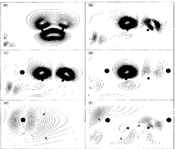
band and the metallization of the whole substrate are easily seen in Fig. 3. The charge-density contour plots ofthe clean substrate in the surface plane [Fig.3(a)]
show the chain structure with the bond charge between surface silicons. In a plane above the surface the charge density is lower, but the corrugation due to the chain structure is maintained [Fig.3(b)].
At6=1
and6=2,
we observe enhance-ment of charge density over the chain atoms with maxi-ma corresponding to surface silicons [Fig.3(c)].
Partial filling of the conduction-band states ate=2
leads to further modifications in the charge distribution [Fig.3(d)].
Note that K atoms at the charge-density hole mimic the zigzagz
chain. The unsupported K layer with two K atoms in the same lattice registry as the overlayer, on the other hand, gives rise to a chain ofhigher charge density at the opposite side ofthe surface unit cell. Thisis where the charge would be found ifthe overlayer were metallized. A clear picture
of
the binding and the posi-tion ofthe K atom relative to the surface charge distri-bution is illustrated in Fig.3(e).
In this vertically cut plane, two holes ofthe surface charge density lie at bothJyg/&JJaq~qiggg~ (a)
l
'IIPR~H~s&i(l' (c) RV~@jan.
) (c) I ))~
((c&Pj)r (((.. )jjj))&))~
(e) (((+C+~+c4( ':)jibjjijii! -~~~i)jj/jFIG.2. Charge-density contour plots ofthe states at I in a
vertical plane passing through a surface Si
—
Si bond: (a) x state; (b) rc* state ofthe cleanSi(111)-(2x
1); (c)m* state ate=
1; (d) z* state ate=2;
(e) s state ofthe unsupported Klayer; (f)a surface resonance above EFat
e=2.
The contourspacing is0.000213a.u.
FIG. 3. Contour plots of the total charge density. (a) Charge density of the clean
Si(111)-(2x
1) in the surfaceplane. In a horizontal plane 4a.u. above the surface, (b) clean
surface, (c) one-K-adsorbed surface, (d) two-K-adsorbed
sur-face. In a vertical plane passing through the surface Si
—
Sibond, (e)two-K-adsorbed surface. Contour spacings are 0.005
a.u. for (a), 0.000213 a.u. for
(b)-(d),
and 0.00448 a.u. for(:).
VOLUME 58, NUMBER 19
PHYSICAL
REVIEW
LETTERS
11MAY 1987sides
of
the surface Si—
Si bond, where two K atoms are located at6
=2.
From the analysis of the electronic structure and charge density, it becomes clear that even at the satura-tion coverage the potassium atoms do not form metallic bonds. This prediction contrasts Si surfaces with metal surfaces, which are known to allow for the metallization ofthe alkali-metal overlayer at high coverage. Earlier, the onset of electron-energy-loss spectroscopy peaks at
8=0.
5 for the K-adsorbedSi(001)-(2X
I)
surface were interpreted to imply that the 1D plasmon excitation of the overlayer was undergoing a Mott transition. Howev-er,Si(001)-(2X 1)
has an empty band lying totally in the band gap, and calculations show that the metallic char-acter attributed to the overlayer is,in fact, the metalliza-tionof
the surface-state band. As noted, here the in-teraction between K andSi(111)
is diAerent, and the novel aspect is that beyond a threshold coverage not only the surface but also the silicon substrate undergoes a me-tallic transition. Recently, Ishida, Terakura, and Tsuka-da' reported a linear combination of atomic orbitals band calculation of the same system. Their conclusions on the metallization are at variance with the present re-sults, perhaps because of the limited basis set and the unoptimized geometry they employed in their study.In summary, we have investigated the K-adsorbed
Si(111)
surface as a function of coverage. We have shown that, because of the existenceof
the active surface-state band, bonding is strong and ionic. At the initial coverage, electrons donated by K atoms fill the z band and yield a 1Dmetallic chain. An important result of this study is that above a threshold coverage, alkali-metal electrons are accommodated by the substrateconduction-band states. This leads to a change in the dimensionality ofthe metallic system from 1 to 2 (or to 3
in a thick substrate) and results in an enhanced conduc-tivity perpendicular to the surface. Moreover, in a thin Si substrate with a positively charged surface conduction-band electrons are expected to create a quan-tum regime similar toone usually obtained in a
selective-ly doped semiconductor superlattice. Finally, since the concentration
of
itinerant electrons in the conduction band can be controlled, one may envisage creating a de-generate semiconductor without the artifacts of bulk al-loying.'
Permanent address: Department ofPhysics., BilkentUni-versity, Ankara, Turkey.
Permanent address: Almaden Research Center, Mail Stop K33/801, 650Harry Road, San Jose, CA95120.
'K.C.Pandey, Phys. Rev. Lett. 47, 1913
(1981).
~M. Schluter,
J.
R. Chelikowsky,S.
G. Louie, and M. L. Cohen, Phys. Rev. B12,4200 (1975),3S. Ciraci and I. P. Batra, Phys. Rev. B33,4294
(1986).
4J. E.Northrup and M. L.Cohen, Phys. Rev. Lett. 49, 1349 (1982).
5H. Tochihara, M. Kubota, M.Miyao, and Y.Murata, Surf. Sci. 158, 497
(1985).
6I.P. Batra and S.Ciraci, Phys. Rev. B33,4312 (1986). 7A. U. MacRae, K. Muller,
J. J.
Lander,J.
Morrison, andJ.
C.Phillips, Phys. Rev. Lett.22, 1048(1969).
SH. Tochihara, Surf. Sci.126,523 (1983); T.Aruga, H. To-chihara, and Y.Murata, Phys. Rev. Lett. 53,372 (1984).
9S.Ciraci and I. P. Batra, Phys. Rev. Lett. 56, 877
(1986).
' H. Ishida, K.Terakura, and M. Tsukada, Solid State
Com-mun. 59,365 (1986).