Full Electrostatic Control of Nanomechanical Buckling
Selcuk Oguz Erbil,1 Utku Hatipoglu ,1 Cenk Yanik,2 Mahyar Ghavami ,1 Atakan B. Ari ,1,† Mert Yuksel,1 and M. Selim Hanay 1,3,*
1Department of Mechanical Engineering, Bilkent University, 06800, Ankara, Turkey 2
Sabancı University SUNUM Nanotechnology Research Center, 34956, Istanbul, Turkey 3National Nanotechnology Research Center (UNAM), Bilkent University, 06800, Ankara, Turkey
(Received 6 September 2019; published 31 January 2020)
Buckling of mechanical structures results in bistable states with spatial separation, a feature desirable for sensing, shape configuration, and mechanical computation. Although different approaches have been developed to access buckling at microscopic scales, such as heating or prestressing beams, little attention has been paid so far to dynamically control all the parameters critical for the bifurcation—the compressive stress and the lateral force on the beam. Here, we develop an all-electrostatic architecture to control the compressive force, as well as the direction and amount of buckling, without significant heat generation on micro- or nanostructures. With this architecture, we demonstrated fundamental aspects of device function and dynamics. By applying voltages at any of the digital electronics standards, we have controlled the direction of buckling. Lateral deflections as large as 12% of the beam length were achieved. By modulating the compressive stress and lateral electrostatic force acting on the beam, we tuned the potential energy barrier between the postbifurcation stable states and characterized snap-through transitions between these states. The proposed architecture opens avenues for further studies in actuators, shape-shifting devices, thermodynamics of information, and dynamical chaos.
DOI:10.1103/PhysRevLett.124.046101
The advent of nano-electromechanical systems (NEMS)
[1,2] has opened promising new perspectives for the
development of sensors [3–6] and mechanical computers
[7–15], owing in particular to their potential for high-speed operation, their scope for large-scale integration, and their robustness in harsh environments[14,16]. The use of buckling instability can increase the resolution of sensors
[17], decrease the footprint of microrelays[18], reduce the operational complexity of memory devices [10,19–21], tune the characteristics of optomechanical devices[22,23], and potentially probe Coulomb blockade in suspended structures[24,25]. Buckling mechanisms play an important role for smart materials [26], morphable microelectronic devices [27], nonreciprocal metamaterials [28], energy harvesters [29], and biomechanical organization [30] and development[31,32].
Despite the important role it plays in such diverse mechanisms, a precise, dynamical, and all-electronic con-trol of buckling bistability has not been demonstrated at the micro- and nanoscale so far. Buckling at this scale has often been accomplished by using beams prestressed during microfabrication [19,20]; however, this approach is not suitable for dynamically controlling the compressive stress on the beam and tuning the potential energy land-scape at will. Another common approach has been to induce buckling thermally, which creates an excessive amount of heating (tens of Kelvins) and power consump-tion (∼mW=compression) which are prohibitively high
for applications [10,33]. Only very few studies have shown nonthermal and tunable buckling either at much larger dimensions [34] or by using special piezoelectric materials[18].
It is striking that while sophisticated techniques have been developed to tailor the dynamics of nanomechanical resonators, another fundamental physical system—the double-well potential—has almost been omitted from such vigorous development so far. Here we sought to fill this gap by introducing a buckling device which can then be used in any nanomechanical experiment that requires a tunable double-well potential. Such systems have been proposed to implement qubits[35]. Moreover, the intricate connection between information theory and entropy[36,37]requires an information processing platform that can operate near thermal energy levels. Only a few experimental protocols, such as one with microparticles in optical traps [38], have achieved such a sophisticated level of control so far. Nanomechanical systems provide another important technology and the platform developed here presents an important advance along the goal of creating controllable nanomechanical double-well potentials.
To address the considerations above, we developed a technique for controlling the buckling parameters without significant heat generation and solely through the appli-cation of dc voltages. We electrostatically controlled the compressive stress and lateral force on a slender nanobeam, and thereby demonstrated various device operations that
PHYSICAL REVIEW LETTERS 124, 046101 (2020)
conceptually and quantitatively prove the high controllabil-ity of buckling-based nanoelectromechanical devices. We showed that the beam can be used as a nanomanipulator reaching maximum displacements as large as 12% of the beam length towards each side, which enables us to investigate the postbuckling behavior and snap-through characteristics of a nanobeam exhibiting high deflection.
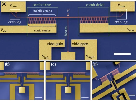
The device structure and operation are as follows [Fig.1(a)]. The device is composed of four main compo-nents: a beam whose buckling is controlled; an inverted comb drive actuator to generate compression and initiate buckling; a modified crab leg spring for recovering back to the unbuckled state; and side gates for controlling the buckling direction. The structural material is p-doped silicon, and the metallization layer is gold (fabrication is detailed the Supplemental Material[39], Sec. II). The beam is 150 nm wide, 250 nm thick, and 40 μm long. The inverted comb drive actuator is composed of interdigitated finger electrodes, and used for axial force generation (P) on the beam to initiate buckling. The comb drive actuator[40]
consists of a stationary and a mobile comb which are controlled by two dc voltages,VstatandVmov, respectively. The mobile part is mechanically and electrically connected to the beam. Modified crab leg design supports the structure and provides a restoring mechanism when the comb drive voltages are nulled [40]. Side gates are placed near the beam for generating a transverse force on the beam by
applying dc voltages (VleftandVright) just before the onset of buckling to preload and guide the beam to the desired buckling direction (left or right). The buckling direction is thus controlled as shown in Fig. 1(b), Fig. 1(c), and the Supplemental Material, video S1[39]. An isometric view of the suspended device is shown in Fig.1(d).
To confirm that the postbuckling behavior can be predicted accurately, we solved a theoretical model of the device operation and compared it with deflection measurements performed under SEM (Fig.2). Since buckling is seen as an effect to avoid in the practice of engineering, theoretical investigations of postbuckling behavior have only taken off during the last decade. Our model for the postbuckling regime considers the force generated by the combs, the large deformation of the beam, and the elastic response of the force-transmission components such as the bar connecting the comb drive to the beam. The model successfully predicts the buckling threshold and postbuckling curve (Supplemental Material[39], Sec. VI). Accurate modeling is critical since the displacement strongly depends on the comb drive voltage: the electrostatic force scales with the square of the comb drive voltage: (Vstat− Vmov)[41]. In this
way, the nanomechanical device can operate at large dis-placements with high precision (as steep as∼1 nm per mV, Fig.2, and video S2 [39]). The central point of the beam displaces more than∼2.8 microns by changing the voltage merely by ∼4 V after the buckling threshold [Fig. 2(b)].
(a)
(b) (c) (d)
FIG. 1. Electrostatic control of buckling. (a) The mechanical and electrical components of the device are labeled on the figure. Buckling is initiated on the beam through the compression force (P) generated by comb drives through the application of VmovandVstat. To control the direction of buckling, side gates are placed with separate control voltagesVleft andVright. By adjusting the side gate voltages right before the axial compression, controlled buckling to the left (b) and to the right (c) can be accomplished. The devices in (b),(c),(d) are slightly different than the one shown in (a), as an extra pair of side gates are incorporated for electronic readout. (d) Isometric view of the device. Scale bars are20 μm for (a),(b), and (c), and 10 μm for (d). SEM images are colorized for clarity.
We note that if the same device was used as a resonator, the maximum amplitude would be limited at 150 nm for the usual linear regime operation, which is about 20 times smaller than the displacements reached here.
The device operation was observed with an SEM system equipped with electrical feedthroughs to apply dc voltages on the two comb drives and the side gate electrodes. A custom-designed control panel was used to handle and measure the supply and control voltages, and was additionally equipped with a programmable microcontroller circuit so that desired voltage waveforms can be applied accurately on the device (Supplemental Material [39], Sec. III). The control of the device was accomplished entirely using dc voltages to generate electrostatic fields only. This is in contrast with thermally induced buckling [10,33], which increases the temperature of the device by tens, in some cases hundreds, of Kelvins and consumes large power.
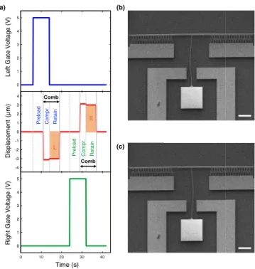
We performed experiments to induce symmetry-breaking during device operation. The experimental protocol consists of three steps: preload, compression, and retain [Fig.3(a), video S3 [39]]. In the preload stage, the guiding voltage which eventually determines the buckling direction is pro-vided by the side gate electrodes where the beam remains unbuckled. During the compression stage, the comb drive is actuated to initiate the buckling on the beam, while the side gate voltage is still kept active to maintain a broken symmetry. In the absence of a control voltage, even the slightest asymmetry in the electrostatic pull of the side gates can bias the buckling direction unpredictably, as the system encounters the pitchfork bifurcation [42]. A finite control voltage therefore biases the buckling in a unique direction, so that the influence of the environmental noise is no longer critical. After the compression step, the retain step begins where the side gate voltage is brought back to zero; therefore the signal representing the original buckling direction is removed. Although the beam pulls back slightly, it none-theless remains deflected in the same direction. We have tested various side gate voltages (5, 3.3, 2.5, and 1.8 V), and in all cases the buckling direction was determined success-fully, which indicates that breaking the symmetry even
slightly can be decisive in the buckling direction (Video S1[39]). Moreover, we have observed that a side gate voltage as low as 0.5 V is sufficient to determine the buckling direction [Figs. 3(b)–3(c), video S4 in Ref. [39]] in the designs with longer side gates positioned near the center to increase capacitive coupling.
The device design enables us to change the potential energy landscape of the beam using the control voltages [Figs.4(a)–4(b)]. The barrier height between the bistable states can be tuned by changing the (Vmov− Vstat), and the
asymmetry between the states can be modified by adjusting the (Vright− Vleft) as shown schematically in Figs.4(a)–4(b)
(details are in the Supplemental Material [39], Sec. VI). We note that the ability to dynamically tune the axial force enables us to control the tradeoff between the minimum side gate voltage used for writing information and the writing and storage fidelity. Smaller potential barrier heights can result in the use of smaller side gate voltages to write information; however, the storage system becomes more sensitive to the external noise. The limiting factor for
40 42 44 46 48
Voltage Difference in Comb Drive (V)
0 0.5 1 1.5 2 2.5 3
Maximum Deflection of the Beam (
µ
m)
(a) (b)
FIG. 2. Post-buckling behavior. (a) Displacements can be controlled by changing the comb drive voltage. Here multiple SEM images are overlaid to show the degree of control possible for positioning of the beam. The scale bar is 5 μm. (b) Post-buckling curve, theory (green) and obtained data (blue).
(a) (b)
(c)
FIG. 3. Controllable symmetry breaking with nanoscale buck-ling. (a) Protocol to control the buckling direction of the device. The top (bottom) panel shows the right (left) side gate control voltage waveform, while the middle panel shows the deflection of the center of the beam as measured under SEM. The black arrow indicates when the comb drive actuators are activated. The shaded region (Retain) shows the postbifurcation state where the control signal is removed but the beam retains its buckling direction. (b), (c) Demonstration of sub-1 V guiding where the buckling direction can be controlled just by applying 0.5 V on the left gate in (b) and the right gate in (c). Supplemental Material, video S4 [39] shows the dynamics of the process; the scale bars are10 μm.
the minimum side gate voltage, apart from fabrication asymmetries, is that the thermomechanical noise in the force domain becomes comparable to the force gen-erated at low control voltages. For instance, when 0.5 V is used as side gate voltage, it is apparent in some frames in video S4 of Ref.[39](e.g., at 10 sec) that the beam initially attempts to buckle towards the opposite direction of the control voltage, as in this case Fside gate¼ 25 and
Fnoise rms¼ 12 pN. Another issue about the controllability
of the system is the coupling between the two mechanical subsystems, the buckling beam and the movable part of the comb drive. However, this interaction is not expected to change the controllability of the buckled beam significantly for the devices reported here, as shown in the Supplemental Material [39], Sec. IX.
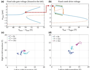
After the bifurcation point, the system adopts two distinct stable states with theoretically symmetrical energy levels. By applying lateral force in the deflection direction, it is possible to reshape the potential energy landscape of the beam so that one energy minimum gets shallower while the other gets deeper [Figs.4(c)–4(d)]. Depending on the comb voltage difference, bistability can be lifted by applying a sufficient lateral force; in other words, the system snaps through. In this case, one of the original stable
states becomes unstable as bending (due to the large lateral force) dominates buckling. Snap-through transition can also be realized while the system still has two distinct stable states. If the relative energy of the shallower well approaches to a value comparable to the noise level— namely, thermomechanical noise or electric noise induced by instruments used, e.g., power supply or electron gun of the SEM—beam tends to experience a sudden jump towards the other minima.
Snap-through transitions provide a direct mechanism to jump between different states. An initial bias provided by lateral forces changes the bifurcation diagram so that only one of the branches is directly accessible as the compression force increases [as indicated by the red dot in Fig. 5(a)]. Once the system is buckled, snapping it to the opposite branch can be accomplished by applying a lateral force in the opposite direction. One way to regard snap-through in this static representation is that the transitions occur when the displacement versus the voltage curve has infinite slope [Fig. 5(b)], although the exact dynamics of snap-through mechanism is still an active research problem[43]. Earlier studies with thermal-induced microscale buckling devices showed that snap-through transitions exhibit a hysteresis curve where the forward and backward jumps occur at different gate voltages[10]. As the device dimensions are shrunk further as in our case, the hysteresis between the left and right transitions are expected to be augmented due to
(a) (b)
(c) (d)
FIG. 4. Tuning the potential energy landscape (a) The potential energy barrier can be adjusted by changing the compressive force throughVmovand Vstatwhich directly affects the energy differ-ence between the zero-deflection state and the two buckling state wells. (b) The asymmetry between the wells can be adjusted by changing the lateral force through Vright and Vleft (assuming a constant beam voltage). (c) Numerical analysis for the case where comb voltage difference is 50.5 V, and varying side gate voltage difference. Loss of bistability occurs after 15 V and system collapses to the right buckling state. (d) Numerical analysis for the case with 51 V comb voltage difference, and varying side gate voltage difference. Since the potential barrier is much deeper, even a 20 V gate voltage difference cannot disrupt bistability. For (c) and (d), energy that corresponds to the zero-deflection position of the unbuckled state is fixed as the datum.
(a) (b)
(c) (d)
FIG. 5. Snap-through transitions between bistable states, in-duced by side gate voltage difference. (a) Bifurcation diagram under a slight lateral bias. (b) Lateral voltage vs displacement curve. Snap-through jumps occur when the slope approaches infinity. Orange arrows show sudden jumps between left and right states. (c),(d) Experimental data for 52.5 and 53 V comb voltage difference. By applying 3 different triangular waveforms to the left gate—changing from 0 to 20 V with 8, 12, and 16 s periods— snap-through transition voltages are recorded (details in Supple-mental Material S8 and video S5 [39]). As the dwell time increases, the amount of hysteresis decreases.
fabrication imperfections at the nanoscale [44]. However, our experiments show that snap-through transition voltages exhibit little hysteretic behavior for higher frequency tran-sitions, and while getting closer to dc, hysteresis disappears. As it is demonstrated in Figs. 5(c)–5(d), data points are confined along the y ¼ x axis while excitation frequency gets lower. This phenomenon can be interpreted as rate-dependent hysteresis[45]. The emergence of rate-dependent hysteresis can be understood by looking at the potential energy landscape of the post-bifurcation states. While buckled, the system adopts two stable states which are separated by an energy barrier. One can adjust the energy barrier by simply applying a force along the deflection direction and eventually the beam ends up jumping from one stable state to the other. However, since there are always noise sources that induce force or displacement fluctuations in the system, the beam becomes more susceptible to switch to the other stable state when barrier gets lowered. If the gradual increase of lateral force is performed slowly, it becomes more probable for the noise processes to bridge the gap between the states, and hence the transitions occur at well-defined voltage values. Nonetheless, a fast-varying lateral force yields more uncertainty near the jump condition which increases the dispersion in the transition voltages. In a perfectly symmetrical system without any physical defect, it is expected to observe identical transition voltages between states. Small vacancies in the silicon device layer and other fabrication related defects lead to an uneven transition behavior in the studied devices by breaking the symmetry between the minimum energy states. In the aforementioned experiment, these dynamically evolving discrepancies in the beam create a transition voltage dispersion that makes a potential hysteresis behavior hard to detect even in higher frequencies. Unlike larger scale systems, these dynamically evolving defects at the nanoscale are more effective on the stress field which provides a continuously changing energy landscape[46].
Snap-through voltages increase, as the comb voltage difference increases: this is because, the height of the potential barrier between two wells increases [Figs. 5(c)–5(d)]. Moreover, during the experiments, the rate of change of applied voltages and the waiting times in each state are observed to be crucial for the determination of critical snap-through voltage since these parameters can affect the material structure of the beam and comb mechanism plasti-cally (as verified by independent experiments). Keeping the beam largely buckled during snap-through transitions impairs the symmetry between bistable states. Thereby, the potential energy landscape of the system varies dynamically during the experiment. Higher potential wells are observed to be responsible for the amplification of the symmetry impairment caused by dwelling in each stable state, a trend observed experimentally as in Figs.5(c)–5(d). For instance, doubling the dwell time reduces the dispersion of transition voltage more than 3 times (Supplemental Material[39], S8).
In this study, a nanomechanical platform to study the dynamics near bifurcations has been developed. For such explorations, the tunability of the compressive force, with-out heating up the device, is critical for tuning the potential energy landscape as desired. Building on the device paradigm here, the nanoscale control of buckling and snap-through transitions between bistable states of struc-tures through electrostatic fields have been accomplished and a rate dependent hysteresis behavior is observed. Such bidirectional electronic control over a nanobeam through buckling can be very practical for configurable optome-chanical systems as well as metamaterials and morphable structures with individually addressable subunits [47]. Using the proposed device as the building block of such tunable or shapeshifting nanoscale metamaterial provides operational flexibility and renders various novel applica-tions possible. Moreover, the ability to precisely tune state separation energy with a monolithic, nanoscale system can enable new physical investigations to be conducted on nonequilibrium statistical mechanics and thermodynamics of information.
We thank the Bilkent UNAM staff for their help with microfabrication (Mustafa Güler and Semih Bozkurt). We thank METU MEMS for help with microfabrication (Ahmet Murat Yağcı, Akın Aydemir, Orhan Akar, Haluk Külah). We thank Mehmet Yılmaz, Arda Seçme, Hande Aydoğmuş, and Matt LaHaye for useful discussions. This work was supported by the European COSTAction IC 1405: Reversible Computation—Extending Horizons of Computing. This work was supported by the Scientific and Technological Research Council of Turkey (TÜBİTAK), Grant No. EEEAG-115E833. M. S. H. acknowledges fellowship support from TÜBA and The Science Academy, Turkey. The manuscript was written through contributions of all authors. All authors have given approval to the final version of the manuscript. M. S. H. conceived the idea. S. O. E. and U. H. designed the devices and performed all the experiments. The fabrication was done mainly by C. Y., with additional support and prototyping by S. O. E., U. H., and A. B. A. M. G. performed the theoretical calculations. M. Y. and M. S. H. performed the initial calcu-lations and device design.
S. O. E. and U. H. contributed equally to this work.
*Corresponding author.
†Present address: Boston University, Boston, Massachusetts,
USA.
[1] H. G. Craighead, Nanoelectromechanical systems,Science 290, 1532 (2000).
[2] M. Roukes, Nanoelectromechanical systems face the future,
Phys. World 14, 25 (2001).
[3] A. Naik, M. Hanay, W. Hiebert, X. Feng, and M. Roukes, Towards single-molecule nanomechanical mass spectrom-etry, Nat. Nanotechnol. 4, 445 (2009).
[4] M. S. Hanay, S. Kelber, A. Naik, D. Chi, S. Hentz, E. Bullard, E. Colinet, L. Duraffourg, and M. Roukes, Single-protein nanomechanical mass spectrometry in real time,
Nat. Nanotechnol. 7, 602 (2012).
[5] M. Li, H. X. Tang, and M. L. Roukes, Ultra-sensitive NEMS-based cantilevers for sensing, scanned probe and very high-frequency applications,Nat. Nanotechnol. 2, 114 (2007).
[6] L. M. de L´epinay, B. Pigeau, B. Besga, P. Vincent, P. Poncharal, and O. Arcizet, A universal and ultrasensitive vectorial nanomechanical sensor for imaging 2D force fields,Nat. Nanotechnol. 12, 156 (2017).
[7] M. Roukes, in Electron Devices Meeting, 2004. IEDM Technical Digest. IEEE International, San Francisco, CA, USA (IEEE, 2004), p. 539.
[8] S. C. Masmanidis, R. B. Karabalin, I. De Vlaminck, G. Borghs, M. R. Freeman, and M. L. Roukes, Multifunctional nanomechanical systems via tunably coupled piezoelectric actuation,Science 317, 780 (2007).
[9] I. Mahboob and H. Yamaguchi, Bit storage and bit flip operations in an electromechanical oscillator, Nat. Nano-technol. 3, 275 (2008).
[10] D. Roodenburg, J. Spronck, H. Van der Zant, and W. Venstra, Buckling beam micromechanical memory with on-chip readout,Appl. Phys. Lett. 94, 183501 (2009). [11] H. Noh, S.-B. Shim, M. Jung, Z. G. Khim, and J. Kim, A
mechanical memory with a dc modulation of nonlinear resonance,Appl. Phys. Lett. 97, 033116 (2010).
[12] J.-S. Wenzler, T. Dunn, T. Toffoli, and P. Mohanty, A nanomechanical Fredkin gate,Nano Lett. 14, 89 (2014). [13] M. A. A. Hafiz, L. Kosuru, and M. I. Younis,
Microelec-tromechanical reprogrammable logic device,Nat. Commun. 7, 11137 (2016).
[14] T.-H. Lee, S. Bhunia, and M. Mehregany, Electromechani-cal computing at500 °C with silicon carbide,Science 329, 1316 (2010).
[15] R. H. Blick, H. Qin, H.-S. Kim, and R. Marsland, A nanomechanical computer—exploring new avenues of com-puting,New J. Phys. 9, 241 (2007).
[16] J. Lee, M. J. Krupcale, and P. X.-L. Feng, Effects ofγ-ray radiation on two-dimensional molybdenum disulfide (MoS2) nanomechanical resonators, Appl. Phys. Lett. 108, 023106 (2016).
[17] S. An, B. Kim, S. Kwon, G. Moon, M. Lee, and W. Jhe, Bifurcation-enhanced ultrahigh sensitivity of a buckled cantilever,Proc. Natl. Acad. Sci. U.S.A. 115, 2884 (2018). [18] U. Zaghloul and G. Piazza, Highly scalable NEMS Relays with stress-tuned switching voltage using piezoelectric buck-ling actuators,IEEE Trans. Electron Devices 61, 3520 (2014). [19] B. Charlot, W. Sun, K. Yamashita, H. Fujita, and H. Toshiyoshi, Bistable nanowire for micromechanical memory,
J. Micromech. Microeng. 18, 045005 (2008).
[20] L. Medina, R. Gilat, B. R. Ilic, and S. Krylov, Experimental dynamic trapping of electrostatically actuated bistable micro-beams,Appl. Phys. Lett. 108, 073503 (2016). [21] L. Medina, R. Gilat, B. Ilic, and S. Krylov, in Proceedings of
Eurosensors (MDPI, Paris, 2017), p. 277.
[22] M. Bagheri, M. Poot, M. Li, W. P. Pernice, and H. X. Tang, Dynamic manipulation of nanomechanical resonators in the
high-amplitude regime and non-volatile mechanical memory operation,Nat. Nanotechnol. 6, 726 (2011). [23] H. Xu, U. Kemiktarak, J. Fan, S. Ragole, J. Lawall, and J.
Taylor, Observation of optomechanical buckling transitions,
Nat. Commun. 8, 14481 (2017).
[24] G. Weick, F. Von Oppen, and F. Pistolesi, Euler buckling instability and enhanced current blockade in suspended single-electron transistors,Phys. Rev. B 83, 035420 (2011). [25] G. Micchi, R. Avriller, and F. Pistolesi, Mechanical Sig-natures of the Current Blockade Instability in Suspended Carbon Nanotubes,Phys. Rev. Lett. 115, 206802 (2015). [26] N. Hu and R. Burgueño, Buckling-induced smart
applica-tions: recent advances and trends,Smart Mater. Struct. 24, 063001 (2015).
[27] H. Fu et al., Morphable 3D mesostructures and microelec-tronic devices by multistable buckling mechanics, Nat. Mater. 17, 268 (2018).
[28] C. Coulais, D. Sounas, and A. Alù, Static non-reciprocity in mechanical metamaterials, Nature (London) 542, 461 (2017).
[29] R. Harne and K. Wang, A review of the recent research on vibration energy harvesting via bistable systems, Smart Mater. Struct. 22, 023001 (2013).
[30] X. Xie, W. Zhao, H. R. Lee, C. Liu, M. Ye, W. Xie, B. Cui, C. S. Criddle, and Y. Cui, Enhancing the nanomaterial bio-interface by addition of mesoscale secondary features: Crinkling of carbon nanotube films to create subcellular ridges,ACS Nano 8, 11958 (2014).
[31] E. Lejeune, A. Javili, and C. Linder, Understanding geo-metric instabilities in thin films via a multi-layer model,Soft Matter 12, 806 (2016).
[32] E. Lejeune, A. Javili, J. Weickenmeier, E. Kuhl, and C. Linder, Tri-layer wrinkling as a mechanism for anchoring center initiation in the developing cerebellum,Soft Matter 12, 5613 (2016).
[33] M. Chiao and L. Lin, Self-buckling of micromachined beams under resistive heating, J. Microelectromech. Syst. 9, 146 (2000).
[34] S. Abu-Salih and D. Elata, Experimental validation of electromechanical buckling, J. Microelectromech. Syst. 15, 1656 (2006).
[35] S. Savel’ev, X. Hu, and F. Nori, Quantum electromechanics: Qubits from buckling nanobars,New J. Phys. 8, 105 (2006). [36] R. Landauer, Irreversibility and heat generation in the
computing process,IBM J. Res. Dev. 5, 183 (1961). [37] C. H. Bennett, Logical reversibility of computation,IBM J.
Res. Dev. 17, 525 (1973).
[38] A. B´erut, A. Arakelyan, A. Petrosyan, S. Ciliberto, R. Dillenschneider, and E. Lutz, Experimental verification of Landauer’s principle linking information and thermody-namics, Nature (London) 483, 187 (2012).
[39] See Supplemental Material at http://link.aps.org/ supplemental/10.1103/PhysRevLett.124.046101 for addi-tional details on device performance and theoretical derivations.
[40] R. Legtenberg, A. Groeneveld, and M. Elwenspoek, Comb-drive actuators for large displacements, J. Micromech. Microeng. 6, 320 (1996).
[41] V. Kaajakari, Practical MEMS: Design of Microsystems, Accelerometers, Gyroscopes, RF MEMS, Optical MEMS,
and Microfluidic Systems (Small Gear Publishing, Las Vegas, NV, 2009).
[42] L. Perko, Differential Equations and Dynamical Systems (Springer-Verlag, New York, 2002), Vol. 7.
[43] M. Gomez, D. E. Moulton, and D. Vella, Critical slowing down in purely elastic ‘snap-through’ instabilities, Nat. Phys. 13, 142 (2017).
[44] X. Chen and S. Meguid, Snap-through buckling of initially curved microbeam subject to an electrostatic force,Proc. R. Soc. A 471, 20150072 (2015).
[45] J. Oh and D. S. Bernstein, Semilinear Duhem model for rate-independent and rate-dependent hysteresis, IEEE Trans. Autom. Control 50, 631 (2005).
[46] T. Ishida et al., Exceptional plasticity of silicon nanobridges,
Nanotechnology 22, 355704 (2011).
[47] A. Arbabi, Y. Horie, M. Bagheri, and A. Faraon, Dielectric metasurfaces for complete control of phase and polarization with subwavelength spatial resolution and high transmis-sion,Nat. Nanotechnol. 10, 937 (2015).