PROCEEDINGS OF SPIE
SPIEDigitalLibrary.org/conference-proceedings-of-spieA plasmonically enhanced pixel
structure for uncooled
microbolometer detectors
Ozan Erturk
Enes Battal
Seniz Esra Kucuk
Ali Kemal Okyay
Tayfun Akin
A Plasmonically Enhanced Pixel Structure for Uncooled
Microbolometer Detectors
Ozan Erturk
1, Enes Battal
2, 3, Seniz Esra Kucuk
1, Ali Kemal Okyay
2, 3, and Tayfun Akin
1, 41
METU-MEMS Research and Application Center, Middle East Technical Univ., Ankara, Turkey
2Dept. of Electrical and Electronics Engineering, Bilkent University, Ankara, Turkey
3UNAM-National Nanotechnology Research Center and Institute of Materials Science and
Nanotechnology, Bilkent University, Ankara, Turkey
3
Dept. of Electrical and Electronics Engineering, Middle East Technical Univ., Ankara, Turkey
ABSTRACT
This paper introduces a method of broadband absorption enhancement that can be integrated with the conventional suspended microbolometer process with no significant additional cost. The premise of this study is that electric field can be enhanced throughout the structural layer of the microbolometer, resulting in an increase in the absorption of the infrared radiation in the long wave infrared window. A concentric double C-shaped plasmonic geometry is simulated using the FDTD method, and this geometry is fabricated on suspended pixel arrays. Simulation results and FTIR measurements are in good agreement indicating a broadband absorption enhancement in the 8 µm - 12 µm range for LWIR applications. The enhancement is attained using metallic geometries embedded in the structural layer of the suspended microbridge, where the metallic-dielectric interface increases the average absorption of a 35 µm pixel from 67.6% to 80.1%.
Keywords: Microbolometer, long wave infrared, surface plasmons, wideband, absorber, reflection suppression, nanoresonator.
1. INTRODUCTION
Microbolometers are the most common room temperature infrared (IR) imaging elements used today. Recent developments in microbolometer design pave the way for performances that were previously possible with only cooled technologies [1]. In addition to cost advantage of microbolometers compared to cooled detectors, the increasing market volume of low-cost infrared imaging systems demands cost effective and high performance microbolometers. The requirements for better quality imagers push for smaller pixel pitch for higher spatial resolution at the expense of lower radiation flux.
One of the most crucial figures of merit of an infrared imaging array is the noise equivalent temperature difference (NETD), usually expressed for the entire focal plane array. The smaller the NETD, the better the performance of the array since it physically signifies the minimum distinguishable temperature difference in a scene.
= 4(f ⋕⁄ ) + 1 V
ℜ τ A (ΔP ΔT⁄ ) (1)
Equation 1 is the NETD expression in terms of the voltage responsivity (ℜV), where (f/#) defines the f -number of the
lens, Vn is the total RMS noise voltage of the system, τ0 is the transmittance of the optics, and AD is the pixel area. The
(ΔP/ΔT)λ1- λ2 term implies the change of power per unit area radiated in the specified spectral range by a blackbody at
temperature T. This is a material and geometry independent property; however, ℜV is linearly proportional to the
absorption coefficient of the pixel. Therefore, infrared imaging systems with even better performances require efficient infrared absorbers integrated with the conventional microbolometer design, in order to account for the decreasing pixel sizes.
Infrared Technology and Applications XXXIX, edited by Bjørn F. Andresen, Gabor F. Fulop, Charles M. Hanson, Paul R. Norton, Proc. of SPIE Vol. 8704, 87041E · © 2013 SPIE
CCC code: 0277-786X/13/$18 · doi: 10.1117/12.2019540 Proc. of SPIE Vol. 8704 87041E-1
The most common structural material for the current microbolometers is silicon nitride due to its thermal and mechanical properties. Considering the refractive index and the extinction coefficient of this material, one can deduce that it is a relatively good absorber around wavelength of 11 µm, which also makes silicon nitride a befitting material for the long wave infrared (LWIR) imaging. However, a suspended silicon nitride slab is a poor absorber in the lower half of the LWIR range. It is desirable to enhance the absorption of silicon nitride layer in the long wave infrared window, especially in the 8 µm – 10 μm range for imagers with lower NETD values. Increasing the thickness of the silicon nitride membrane may provide higher absorption; however, such a design would suffer from increased thermal time constant due to a larger mass and therefore lower frame rates of the imager.
The most commonly used methods to increase the absorption in an active layer are anti-reflective coatings (ARCs) [2], optical cavities [3,4] and resonators [5,6]. For ARCs, perfect matching is rarely possible using layers with constant refractive index, and also fabrication of layers having a gradient refractive index profile is highly complex [7]. For optical cavities and resonators, the structure dimensions have to be on the order of the wavelength of the incident light [8], which is not desirable considering the downscaling of the pixel sizes in the ongoing road-map of imaging technologies. Recently, surface plasmons (SPs), collective oscillations of free electrons coupled with an electromagnetic wave on a metal/dielectric interface, have been widely used for enhanced absorption from ultraviolet (UV) [9] up to mid-infrared (MIR) [10] wavelengths. Localization property of surface plasmons at sub-wavelength dimensions makes them very attractive for absorption enhancement purposes, especially in imaging technologies due to decreasing pixel size [11,12].
This paper presents the design and the implementation of metallic decorations on conventional microbolometer arrays utilizing plasmonic resonance for field enhancement in the structural layer, and it demonstrates that the spectral absorption of the microbolometer can be engineered to improve the overall absorption in the 8 µm – 12 μm range. It should be pointed out that fabricating plasmonic features in the pixels comes with almost no additional processing cost or complexity. As a result, the feasibility of integration of plasmonic structures into the microbolometer process as well as its aptness in the wavelength of interest makes them an excellent candidate for broadband absorption enhancement.
2. BOLOMETER FABRICATION AND DECORATING WITH METALLIC RESONATORS
A microbolometer pixel is a suspended microbridge with a resistor on the top. Figure 1 shows 3D illustration of the microbolometer pixel structure used in this study. A simple suspended silicon nitride microbridge is used to model a microbolometer pixel since it is the primary absorber layer.
In our previous study [13], we computationally investigated concentric double C-shaped gold features for broadband absorption enhancement in the LWIR region. In this study, microbolometer pixels integrated with plasmonic structures are fabricated. Figure 2 depicts the plasmonic structures embedded into the silicon nitride layer.
Figure 1: 3D representative view of a simplified microbolometer pixel structure used in this study.
Structural Si3N4
layer
Anchor Support arm
Proc. of SPIE Vol. 8704 87041E-2
H
t't
o
H Ë k k L1)
Px < T Wr
xO
e
Figure 2: 3D representative view of the embedded plasmonic structures.
Figure 3 shows the process flow of the fabrication of the microbolometer pixels decorated with the plasmonic structures. The microbolometer pixel fabrication starts with the formation of a back reflector (mirror) by sputtering a Ti/Au bilayer. Then, a 2-µm-thick polyimide film is spin-coated as a sacrificial layer followed by patterning for the anchor openings. Since the plasmonic metal layer is embedded into the silicon nitride layer, the first 200 nm of the silicon nitride film is deposited preceding a Cr/Au bilayer sputtering. Concentric double C-shaped plasmonic features are patterned using dry etching in an ICP system. The second 200-nm-thick silicon nitride film is used to sandwich the plasmonic structures. In reference pixels, the plasmonic metal layer is completely etched as control samples for comparison purposes. The overall silicon nitride layer of 400 nm thickness is patterned in an RIE system to form the pixel body and support arms. Finally, the pixel is released in O2 plasma to form the suspended microbridge. Figure 4
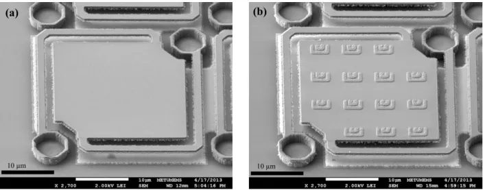
shows the scanning electron microscope (SEM) images of the completed microbolometer pixels with and without plasmonic features.
(a) (b) (c)
(d) (e) (f)
Figure 3: a 3D representative view of the fabrication steps: (a) Ti/Au mirror layer, (b) sacrificial layer with anchor openings, (c) the first silicon nitride structural layer, (d) Cr/Au plasmonic structures, (e) the second silicon nitride structural layer followed by pixel body formation, and (f) suspended pixel with plasmonic structures.
Metal Polyimide Si3N4 Silicon Nitride Chromium/Gold 20 nm / 100 nm 2 µm 200 nm 200 nm
Proc. of SPIE Vol. 8704 87041E-3
10µn METUNEMS 9/17/2013 X 2,700 2.00kV LEI SEM WD 12mn 5:04 :16 PM 10, METUMEMS 4/17/2013 SEM WD 15mm 4:59:15 PM 2.5 2 C d `7) 1.5 o C.7 ó 1
t
0.5 06---k
n- - -ter'
/
1 1 1 /I
/ ! / 1- n V
8 10 12 Wavelength (pm) 14 3.5 3 1 0.5 16Figure 4: Aerial view SEM images of completed pixels: (a) reference pixel and (b) pixel with the embedded plasmonic structures.
3. SIMULATION AND MEASUREMENT COMPARISON
Numerical simulations of both the reference and the plasmonically enhanced structures are performed using FDTD Solutions, Lumerical Inc. The optical constants of the PECVD silicon nitride layer are obtained with a careful characterization using variable angle spectroscopic ellipsometry (IR-VASE Make/Model) (Figure 5). For the metals, previously validated Drude oscillator model parameters [14] are used to model the frequency-dependent permittivity values in the simulations.
Figure 5: Experimentally measured optical data of PECVD silicon nitride used in the numerical simulations. Note the peak of the extinction coefficient of silicon nitride at around 12µm.
Among numerous concentric C-shaped structures, an optimized geometry is chosen for this study. Figure 6 shows an x-y plane view of the simulated structure. In order to handle computational requirements, the optimization is performed considering infinitely periodic unit cells [13]. The optimized plasmonic structure (L1 = 3.5 µm, L2 = 1.5 µm,
L3 = 2.5 µm, W = 1 µm, and T = 0.05 µm) is fabricated as described above. The width of the features is equal to the
gap between the arms of the double C-shapes. Figure 6 also shows the periodicity of the structure, which is determined as Px = 5 µm and Py = 6 µm in the x-direction and y-direction, respectively. Due to fabrication imperfections,
simulation of the pixel is repeated by importing the simulation structure from the SEM image of the completed pixel.
10 µm 10 µm
(a) (b)
Proc. of SPIE Vol. 8704 87041E-4
100 LL 80 0 w-C. 40 o o
á
20 o 8 10 12 Wavelength (um) 14 100 LL 80 0 w-0- 40 o cná
20 o 8 10 12 Wavelength (um) 14Boundary conditions along z-axis are set to be metal boundary and perfectly matching layers for the bottom and the top boundaries, respectively. The boundary conditions in the x-y plane are defined as periodic to simulate the pixel array, where the pixel pitch is given as 35 µm. The injection is assumed along z-axis towards the pixel at a normal incidence. The reflected power, R, from the pixel is monitored, and absorption is calculated by 1-R.
Figure 6: Simulation window in the x-y plane (a) of the full pixel and (b) a unit cell of plasmonic feature as imported from SEM image. Note that the pixel support arms are not included in the simulation of the full pixel.
The fabricated pixel arrays are characterized by measuring spectral reflection, R(λ), using a Bruker Vertex 70 FTIR Spectrometer with Hyperion 2000 Microscope attachment with 15x objective (0.4 numerical aperture). Absorption is calculated as 1 - R (λ) assuming no transmission through the mirror on the bottom. Figure 7 compares the measured and computed spectral responses of both the plasmonically enhanced and the reference pixels. Figure 7 indicates that the simulation results are in accord with the FTIR measurements including the shoulder features between 7.5 µm and 9 µm for both transverse-electric (TE) and transverse-magnetic (TM) polarizations. The offset between the simulation and the experimental results is attributed to increased absorption and scattering due to the support arms, which are not included in the simulations. Since the fill factor (ratio of active area to the pitch area) is identical for both plasmonically enhanced and reference structures, simulations predict valuable comparison between the two.
Figure 7: Comparison of the FTIR measurement results to the numerical simulations. Note the spectral agreement in the reflection trend between experimental and simulated results. The simulated absorption values are lower than the experimental values because the arms are ignored in simulations therefore there is higher reflection from the mirror at the bottom. Plasmonic Reference Exp Sim Exp Sim y x (a) (b) 35 µm 35 µm 6 µm 5 µm
Proc. of SPIE Vol. 8704 87041E-5
,
(a Figure 8 sho 7.3 µm and respectively. outer split-rin between the i inner ring lik wavelength, t like behavior corresponding Figure 8 polarizat Figure 9 show illumination. plasmonic str nitride has a excitation. Figure 9 average a a)ows the electr 7.6 µm wave
For TM polar ng acts like an inner and the o ke a +x direc
the inner and r in total. Suc g polarization 8: Electric field tions at 7.3 µm ws the spectra The plasmon ructure canno a peak (Figur : Experimental absorption in th
+ -
-
ric field maps elengths wher rization at 7.3 n electric qua outer rings, oc ted dipole as the outer rin ch a resonant ns. d intensity pro and 7.6 µm wa al absorption o nic structure in ot provide as re 5), which overall absorp he 8-12µm rang
+ -
+
s of a concen re the absorp 3 µm waveleng adrupole. The ccurring only the side is n g behaves lik behavior in files (|Ez|2) of velengths, resp of the plasmo ncreases the a significant ab causes rapid ption enhancem ge is increased b+
TM E Abs = 8 ntric C-shaped ption enhance ngth, the inner electric quad at the arms. T not affected fr ke two dipoles this structure f the concentric pectively. onically enhan absorption in t bsorption enh decay of sument of the plas by 18.5%. (b) Ez 80.1% Abs = 67.6 d plasmonic f ement is max r split-ring act drupole is form The side of the from the inner s oscillating o e results in str
c double C-sha
nced and the r the entire 7-1 hancement bec rface plasmon smonic arrays c
-
6% feature at illu ximum for TM s like a +x dir med by the st e outer ring os r ring. For TE out of phase, r rong absorptio aped apertures reference struc 4 µm spectrum cause, extincti ns, therefore, compared with+
+
-
+
Enhan Refere umination wav M and TE p rected dipole trong capaciti scillates in ph E polarization resulting in a ion enhancem for (a) TM actures for the um. At around tion coefficien , inhibiting a the reference p
-
TE nced ence velengths of olarizations, whereas the ive coupling hase with the n at 7.6 µm a quadrupole ments for thend (b) TE unpolarized d 12 µm, the nt of silicon any resonant pixels. The E Ez
Proc. of SPIE Vol. 8704 87041E-6
On the other hand, the enhancement is much more significant at around 8 µm where the silicon nitride is an inefficient absorber because it exhibits a low extinction coefficient (Figure 5), that favors the excitation and propagation of surface plasmons. In the spectral region of interest, 8-12 µm, the reference pixel has an average absorption of 67.6% while that for the plasmonically enhanced pixel is increased by 18.5% to an overall 80.1%.
4. CONCLUSION
This paper presents an overall cost-effective absorption enhancement achieved within the most commonly used resistive microbolometer design limitations. We have designed, simulated, and fabricated double C-shaped plasmonic features embedded into a typical microbolometer pixel and showed good agreement between the simulated and measured trends. We established a successful modeling approach where the plasmonic features are designed independently from the physical pixel parameters. This independent design approach enables efficient tailoring the spectral response as desired for arbitrary suspended microbridge designs. As a result of this study, we demonstrated 18.5% overall spectral enhancement in the absorption of a plain reference pixel with the addition of plasmonic features. Such an improvement, with almost no additional processing cost or complexity, is expected to decrease the NETD value of the pixel considerably, paving the way for low-cost and high performance infrared imagers.
REFERENCES
[1] Frank, N., Edvard, K., and Göran, S., “Wafer-level membrane transfer bonding of polycrystalline silicon bolometers for use in infrared focal plane arrays,” Journal of Micromechanics and Microengineering, 11(5), 509 (2001).
[2] Raut, H. K., Ganesh, V. A., Nair, A. S., and Ramakrishna, S., “Anti-reflective coatings: A critical, in-depth review,” Energy & Environmental Science, 4(10), 3779-3804 (2011).
[3] Hernandez, G., “Fabry-Perot with an absorbing etalon cavity,” Appl. Opt., 24(18), 3062-3067 (1985).
[4] Zheng, H. Y., Jin, X. R., Park, J. W., Lu, Y. H., Rhee, J. Y., Jang, W. H., Cheong, H., and Lee, Y. P., “Tunable dual-band perfect absorbers based on extraordinary optical transmission and Fabry-Perot cavity resonance,” Opt. Express, 20(21), 24002-24009 (2012).
[5] Park, Y., Drouard, E., El Daif, O., Letartre, X., Viktorovitch, P., Fave, A., Kaminski, A., Lemiti, M., and Seassal, C., “Absorption enhancement using photonic crystals for silicon thin film solar cells,” Opt. Express, 17(16), 14312-14321 (2009).
[6] Bermel, P., Luo, C., Zeng, L., Kimerling, L. C., and Joannopoulos, J. D., “Improving thin-film crystalline silicon solar cell efficiencies with photonic crystals,” Opt. Express, 15(25), 16986-17000 (2007).
[7] Moore, D. T., “Gradient-index optics: a review,” Appl. Opt., 19(7), 1035-1038 (1980).
[8] Gramotnev, D. K., and Bozhevolnyi, S. I., “Plasmonics beyond the diffraction limit,” Nat Photon, 4(2), 83-91 (2010).
[9] Abiyasa, A. P., Yu, S. F., Lau, S. P., and Leong, E. S. P., “Enhancement of ultraviolet lasing from Ag-coated highly disordered ZnO films by surface-plasmon resonance,” Applied Physics Letters, 90(23), 231106-3 (2007). [10] Jiang, Z. H., Yun, S., Toor, F., Werner, D. H., and Mayer, T. S., “Conformal Dual-Band Near-Perfectly
Absorbing Mid-Infrared Metamaterial Coating,” ACS Nano, 5(6), 4641-4647 (2011).
[11] Park, K. Y., Meierbachtol, C. S., Wiwatcharagoses, N., and Chahal. P., “Surface plasmon-assisted terahertz imaging array,” 2012 IEEE 62nd Electronic Components and Technology Conference (ECTC), pp.1846-1851, (2012).
[12] Lee, S. J., Ku, Z., Barve, A., Montoya, J., Jang, W.-Y., Brueck, S. R. J., Sundaram, M., Reisinger, A., Krishna, S., and Noh, S. K., “A monolithically integrated plasmonic infrared quantum dot camera,” Nat Commun, 2, 286 (2011).
[13] Lulec, S. Z., Kucuk, S. E., Battal, E., Okyay, A. K., Tanrikulu, M. Y., and Akin, T., “An analysis for the broad-band absorption enhancement using plasmonic structures on uncooled infrared detector pixels,” Proc. of SPIE 8353, 83531D (2012).
[14] Bouchon, P., Koechlin, C., Pardo, F., Haidar, R., and Pelouard, J., “Wideband omnidirectional infrared absorber with a patchwork of plasmonic nanoantennas,” Opt. Lett. 37, 1038-1040 (2012).
Proc. of SPIE Vol. 8704 87041E-7