Photovoltaic nanocrystal scintillators
hybridized on Si solar cells
for enhanced conversion efficiency in UV
Evren Mutlugun, Ibrahim Murat Soganci, and Hilmi Volkan Demir
Department of Physics, Department of Electrical and Electronics Engineering, Nanotechnology Research Center, Institute of Materials Science and Nanotechnology, Bilkent University, Bilkent, Ankara, Turkey 06800
Abstract: We propose and demonstrate semiconductor nanocrystal based
photovoltaic scintillators integrated on solar cells to enhance photovoltaic device parameters including spectral responsivity, open circuit voltage, short circuit current, fill factor, and solar conversion efficiency in the ultraviolet. Hybridizing (CdSe)ZnS core-shell quantum dots of 2.4 nm in diameter on multi-crystalline Si solar cells for the first time, we show that the solar conversion efficiency is enhanced 2 folds under white light illumination similar to the solar spectrum. Such nanocrystal scintillators provide the ability to extend the photovoltaic activity towards UV.
©2008 Optical Society of America
OCIS codes: (250.0250) Optoelectronics; (260.7190) Ultraviolet; (160.2540) Fluorescent and luminescent
materials; (040.6040) Silicon; (040.5350) Photovoltaics; Semiconductor nanocrystals, Quantum dots.
References and links
1. P. Clarke, “Booming photovoltaic market expected to aid wafer makers,” (EE Times, 2005), http://www.extremenetworks.com/technology/whitepapers/vMAN.asp.
2. B. Sun, H. J. Snaith, A. S. Dhoot, S. Westenhoff, and N. C. Greenham, “Vertically segregated hybrid blends for photovoltaic devices with improved efficiency," J. Appl. Phys. 97, 014914 (2005).
3. X.-F. Li, Y.-R. Chen, J. Miao, P. Zhou, Y.-X. Zheng, and L.-Y. Chen, “High solar absorption of a multilayered thin film structure,” Opt. Express 15, 1907-1912 (2007).
4. S. M. Sze, Semiconductor Devices: Physics and Technology (Wiley and Sons Inc., 1985). 5. P. Bhattacharya, Semiconductor Optoelectronic Devices (Prentice Hall, 1997).
6. A. Pauchard, A. Rochas, Z. Randzelovic, P. A. Besse, and R. S. Popovic, “Ultraviolet avalanche photodiode in CMOS technology,” IEDM Tech. Dig. 709-712 (2000).
7. International program on chemical safety, “Ultraviolet radiation” http://www.inchem.org/documents/ehc/ehc/ehc160.htm.
8. M. M. Caldwell, “Plant life and ultraviolet radiation: some perspective in the history of the earth's UV climate,” BioScience 29, 520-52 (1979).
9. S. Gaponenko, Optical properties of semiconductor nanocrystals (Cambridge University Press, 1998). 10. D. V. Talapin, A. L. Rogach, A. Kornowski, M. Haase, and H. Weller, “Highly luminescent monodisperse CdSe
and CdSe/ZnS nanocrystals synthesized in a hexadecylamine-trioctylphosphine oxide-trioctylphosphine mixture,” Nano Lett. 1, 207-211 (2001).
11. A. L. Rogach, A. Kornowski, M. Gao, A. Eychmu1ller, and H. Weller, “Synthesis and characterization of a size series of extremely small thiol-stabilized CdSe nanocrystals,” J. Phys. Chem. B 103, 3065-3069 (1999). 12. B. O. Dabbousi, J. Rodriguez-Viejo, F. V. Mikulec, J. R. Heine, H. Mattoussi, R. Ober, K. F. Jensen, and M. G.
Bawendi, “(CdSe)ZnS core-shell quantum dots: synthesis and characterization of a size series of highly luminescent nanocrystallites,” J. Phys. Chem. B 101, 9463-9475 (1997).
13. M. A Hines and P. Guyot-Sionnest, “Synthesis and characterization of strongly luminescent ZnS-capped CdSe nanocrystals,” J. Phys. Chem. 100, 468-471 (1996).
14. S. Coe, W.-K. Woo, M. Bawendi, and V. Bulovic, “Electroluminescence from single monolayers of nanocrystals in molecular organic devices,” Nature 420, 800-803 (2002).
15. S. Chaudhary, M. Ozkan, and W. C. W. Chan, “Trilayer hybrid polymer-quantum dot light-emitting diodes,” Appl. Phys. Lett. 84, 2925-2927 (2004).
16. N. Lalic, “Light emitting devices based on silicon nanostructures,” KTH Royal Institute of Technology, Stockholm (2000).
17. S. Nizamoglu, T. Ozel, E. Sari, and H. V. Demir, "White light generation using CdSe/ZnS core-shell nanocrystals hybridized with InGaN/GaN light emitting diodes," Nanotechnology 18, 065709 (2007). 18. S. Nizamoglu and H. V. Demir, "Nanocrystal based hybrid white light generation with tunable color
parameters," J. Opt. A 9, S419-S424 (2007).
19. S. Nizamoglu and H. V. Demir, "Hybrid white light sources based on layer-by-layer assembly of nanocrystals on near-UV emitting diodes," Nanotechnology 18, 405702 (2007).
20. H. V. Demir, S. Nizamoglu, T. Ozel, E. Mutlugun, I. O. Huyal, E. Sari, E. Holder, and N. Tian, “White light generation tuned by dual hybridization of nanocrystals and conjugated polymers," New J. Phys. 9, 362 (2007). 21. P. P. Pompa, L. Martiradonna, A. Della Torre, F. Della Sala, L. Manna, M. De Vittorio, F. Calabi, R. Cingolani,
and R. Rinaldi, “Metal-enhanced fluorescence of colloidal nanocrystals with nanoscale control,” Nature Nanotechnology 1, 126-130 (2006).
22. J-H. Song, T. Atay, S. Shi, H. Urabe, and A. V. Nurmikko, “Large enhancement of fluorescence efficiency from CdSe/ZnS quantum dots induced by resonant coupling to spatially controlled surface plasmons,” Nano Lett. 5, 1557-1561 (2005).
23. I. M. Soganci, S. Nizamoglu, E. Mutlugun, O. Akin, and H. V. Demir, "Localized plasmon-engineered spontaneous emission of CdSe/ZnS nanocrystals closely-packed in the proximity of Ag nanoisland films for controlling emission linewidth, peak, and intensity," Opt. Express 15, 14289 (2007).
24. D. Qi, M. B. Fischbein, M. Drndic, and S. Selmic, “Efficient polymer-nanocrystal quantum-dot photodetectors,” Appl. Phys. Lett. 86, 093103 (2005).
25. M. B. Fischbein and M. Drndic, “CdSe nanocrystal quantum-dot memory,” Appl. Phys. Lett. 86, 193106 (2005).
26. I. Gur, N. A. Fromer, M. L. Geier, and A. P. Alivisatos, “Air-stable all inorganic nanocrystal solar cells processed from solution,” Science 310, 462-465 (2005).
27. W. U. Huynh, J. J. Dittmer, and A. P. Alivisatos, “Hybrid nanorod-polymer solar cells,” Science 295, 2425-2427 (2002).
28. A. J. Nozik, “Quantum dot solar cells,” Physica E 14, 115-120 (2002).
29. J. Liu, T. Tanaka, K. Sivula, A. P. Alivisatos, and J. M. J. Fréchet, “Employing end-functional polythiophene to control the morphology of nanocrystal-polymer composites in hybrid solar cells,” J. Am. Chem. Soc. 126, 6550-6551 (2004).
30. E. Mutlugun, I. M. Soganci, and H. V. Demir, "Nanocrystal hybridized scintillators for enhanced detection and imaging on Si platforms in UV," Opt. Express 15, 1128-1134 (2007).
31. Sze S. M., Physics of Semiconductor Devices (John Wiley and Sons., 1981).
32. E. Sari, S. Nizamoglu, T. Ozel, and H. V. Demir, "Blue quantum electroabsorption modulators based on reversed quantum confined Stark effect with blue shift," Appl. Phys. Lett. 90, 011101 (2007).
33. H. V. Demir, V. A. Sabnis, O. Fidaner, J. S. Harris, Jr., D. A. B. Miller, and J.-F. Zheng, "Multifunctional integrated photonic switches," IEEE J. Sel. Top. Quantum. Electron. 11, 86 (2005).
34. H. V. Demir, V. A. Sabnis, J.-F. Zheng, O. Fidaner, J. S. Harris, Jr., and D. A. B. Miller, "Scalable wavelength-converting crossbar switches," IEEE Photon. Technol. Lett. 16, 2305 (2004).
35. V. A. Sabnis, H. V. Demir, O. Fidaner, J. S. Harris, Jr., D. A. B. Miller, J.-F. Zheng, N. Li, T.-C. Wu, H.-T. Chen, and Y.-M. Houng, "Optically-controlled electroabsorption modulators for unconstrained wavelength conversion," Appl. Phys. Lett. 84, 469 (2004).
36. Newport Corp. product catalog, "The Newport Resource 2006/2007 Solutions to Make, Manage and Measure Light, " ( Newport 2006), http://www.newport.com/ .
1. Introduction
Silicon is one of the most abundant elements in the earth’s crust and is currently the most predominantly used material in microelectronics. Today silicon based microelectronic
technology (e.g., complimentary metal oxide semiconductor―CMOS and silicon on
insulator―SOI) offers the ability to fabricate chips with sub-micrometer features in large volumes. In optoelectronics, silicon is also widely used, especially in imaging (e.g., charged
coupled devices―CCDs in the visible). Similarly, silicon finds wide-scale use in
photovoltaics (PV) in optoelectronics. About 95% of the PV market is presently dominated by Si based solar cells [1]. To date there has been a considerable amount of research work on the use of silicon in photovoltaic devices in the literature, especially for improving solar conversion efficiency [2, 3]. Presently, although silicon is used commonly in the PV industry, it is subject to fundamental constraints due to its intrinsic material properties that limit its solar conversion efficiency and related photovoltaic device parameters (including open circuit
voltage, short circuit current, and fill factor). Such one important limitation is its very low responsivity in the ultraviolet (UV) range [4, 5]. Silicon devices typically exhibit two orders of magnitude weaker responsivity in the ultraviolet than that in the visible. This stems from its very high absorption coefficient and the resulting very short absorption length in the UV. Consequently, it becomes very difficult to collect the photogenerated carriers across silicon devices and thus to generate electrical energy under UV illumination. A variety of approaches have been investigated to enhance the responsivity of silicon in UV, e.g., by using shallower junctions in avalanche photodiode architecture [6].
However, the UV part of the solar spectrum (below 400 nm) is crucial because UV makes about 7% of the entire solar spectrum on the earth (after passing through the ozone layer) and 12% in space [7, 8]. Therefore, it is critical to make use of UV spectrum in solar energy conversion both for the roof-top PV power generation on earth and the satellite applications in space. Since silicon itself is not capable of using the UV part of the solar spectrum for solar energy conversion, in this work we propose and demonstrate semiconductor nanocrystal based photovoltaic scintillators integrated on solar cells made of Si to extend their responsivity to the ultraviolet spectral range. In this paper for the first time, we present the concept, design, fabrication, and experimental characterization of such photovoltaic nanocrystal scintillators hybridized on Si solar cells to substantially enhance their photovoltaic device parameters including spectral responsivity, open circuit voltage, short circuit current, fill factor, and solar conversion efficiency. Hybridizing (CdSe)ZnS core-shell nanocrystals (of 2.4 nm in diameter with a ±5% size distribution) on multi-crystalline Si solar cells, we show that the solar conversion efficiency is doubled under white light illumination similar to the solar spectrum on the earth. Such nanocrystal photovoltaic scintillators increase the efficiency of the existing visible photovoltaic devices (e.g., Si solar cells) for use in the solar applications where UV illumination is available (e.g., on earth and in space); this is the added value provided in this hybrid approach.
Nanocrystals find various potential high-technology applications. To date there has been a significant amount of research effort for the synthesis and characterization of such nanocrystal quantum dots [9-13]. Also, the use of nanocrystals in optoelectronic devices is extensively investigated [14-27], owing to their distinctive optical characteristics. Their interesting optical features primarily come from their three dimensional quantum confinement especially as their radii get smaller than the bulk exciton Bohr radius. For example, in nanocrystals, it is possible to fine-tune the optical emission and absorption spectra using the size effect [9], while obtaining relatively narrow emission linewidth with the synthesis of mono-disperse nanocrystals and high quantum efficiencies with the synthesis of the passivating outmost shell layer [10-12]. Among such optoelectronic device applications are nanocrystal LEDs [18-20], hybrid white light sources [17-20], plasmon coupled nanocrystal emitters [21-23], photodetectors [24], optical memories [25], and solar cells [26-29]. Here, yet as another optoelectronic device application for the nanocrystals, we present a proof-of-concept demonstration of photovoltaic scintillators incorporating high-density nanocrystals for extending the photovoltaic activity to the UV.
Previously, there have been different studies for the demonstration of solar cells using nanocrystals [26-29]. For example, in [26], nanocrystal embedded solar cells have been successfully demonstrated, where the nanocrystals were used as the active material to absorb the incident light and to collect the photogenerated carriers. In these solar cells made of nanocrystals, the multiple exciton generation and the resulting enhancement of solar cell efficiency were also observed. Furthermore, in [27], a hybrid nanorod-polymer solar cell has been demonstrated, with its external quantum efficiency studied as a function of the nanoparticle size. Different from the previous literature, in this work we focus on the enhancement of the photovoltaic performance for already fabricated Si solar cells by functionalizing them with the nanocrystal scintillators on the top. Such photovoltaic nanocrystal scintillators hybridized on Si solar cells lead to as high as 2-fold enhancement in the solar conversion efficiency, reported for the first time in the literature to the best of our
knowledge. The use of these photovoltaic nanocrystal scintillators is particularly interesting to leverage today’s advanced Si solar cell technology for enabling operation in the UV.
In our previous work, we developed scintillators using nanocrystals for Si based photodetectors and CCD cameras to enhance their responsivity and to improve detection and imaging characteristics in the UV [30]. For enhanced operation in the UV, we demonstrated the optical imaging of UV spots on CCD cameras hybridized with nanocrystals, which is not possible by using bare CCD cameras. Unlike our previous work, in this letter for the first time, developing nanocrystal scintillators for Si solar cells, we study and demonstrate the nanocrystal hybridization for the enhancement of those device parameters specific only to the solar cells such as the solar conversion efficiency, the open circuit voltage, the short circuit current, and the fill factor.
2. Concept of photovoltaic nanocrystal scintillators
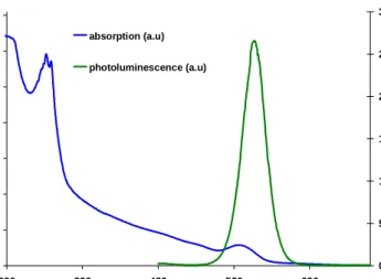
The concept of our nanocrystal scintillator for silicon relies on making use of the high absorption levels of the nanocrystals in the UV (typically 10,000s cm-1) and of the Si solar cells in the visible (in the range of 10,000 cm-1, also in [31]). The operating principle of our nanocrystal scintillator is based in particular on the reduced overlap of the optical absorption and emission spectra of the nanocrystals, mitigating the level of re-absorption. Figure 1 shows the photoluminescence and optical absorption spectra of our (CdSe)ZnS core-shell nanocrystals. The photoluminescence spectrum is measured using a He-Cd laser pump (at 325 nm) and the absorption spectrum is taken using a UV-VIS spectrometer, both at room temperature. These (CdSe)ZnS core-shell nanocrystals, which feature a quantum efficiency of about 15-30%, are 2.4 nm in diameter (with a size distribution of ±5%) and have a corresponding peak emission wavelength of 548 nm. As observed in Fig. 2, the overlap between the emission and absorption spectra of these nanocrystals is very small, as one of the common features of nanocrystals in general. (Also, note that the optical absorption given in Fig. 2 shows a dip around 250 nm, which comes from the measurement setup (spectrophotometer). Indeed the optical absorption keeps increasing at these wavelengths, too.)
In operation, the incident UV photons are first strongly absorbed by the scintillator nanocrystals, generating electron-hole pairs in the nanocrystals. These photogenerated carriers then relax to lower energy states (e.g., through phonon interactions) and recombine radiatively at a lower photon energy with high enough quantum efficiency. Most of these photons that are emitted at longer wavelengths (in the visible around 548 nm by our (CdSe)ZnS nanocrystals) are not absorbed again by the nanocrystals themselves and thus arrive at the active surface of the integrating Si solar cell platform. As a result, these photons are then strongly absorbed by the Si solar cell to contribute to the solar energy conversion. Therefore, the hybridized nanocrystals on the Si solar cell allows the incident UV photons effectively to be converted to visible photons (basically for wavelength up-conversion) to generate electrical energy at the Si photovoltaic platform where the UV photons were otherwise unused. Here the use of nanocrystals in our scintillators also provides an additional advantage to tune their emission wavelength conveniently to match the PV response of the Si solar cell as necessary.
These green-emitting nanocrystals are carefully chosen to have their emission wavelength to fall within the high-responsivity spectral range of the silicon solar cell, while maintaining their high quantum efficiency. Our nanocrystals initially kept in the toluene are mixed with acetone to centrifuge (for 5 min at 13,500 rpm) for the phase separation of the nanocrystals from the toluene solvent. These nanocrystals are then mixed with poly methyl methacrylate (PMMA) to obtain a high nanocrystal concentration (15 µg/nmol). The reasons for blending nanocrystals in a very small amount of polymeric solution include obtaining a high film quality and a sharp edge in the optical absorption spectra of the resulting nanocrystal-polymer thin film. To fabricate our samples, we use standard fabrication techniques similar to those developed and described in our previous optoelectronics device work [17-20, 32-35]. We prepare the nanocrystal-polymer films on our samples on the hot plate (at 50 °C) to achieve uniform films. The nanocrystals are prepared in varying amounts hybridized on the top of Si
solar cells to demonstrate the change in solar cell parameters as a function of the incorporated nanocrystal amount. 0.45 0.95 1.45 1.95 2.45 2.95 3.45 3.95 220 320 420 520 620 wavelength(nm) ab s o rp ti o n ( a .u ) 0 5000 10000 15000 20000 25000 30000 p h ot ol u m in e s e n ce ( a .u ) absorption (a.u) photoluminescence (a.u)
Fig. 1. Photoluminescence and absorption spectra of our green nanocrystals in thin film.
3. Experimental demonstration of photovoltaic nanocrystal scintillators
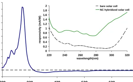
We experimentally study and demonstrate the enhancement in the spectral responsivity of our multi-crystalline silicon solar cells with the use of our nanocrystal scintillators in the UV. We perform this optical characterization by measuring the photocurrent from the Si solar cell before and after the hybridization of the nanocrystal scintillator on the top with an optical chopper/lock-in amplifier setup at room temperature. We obtain the responsivity of the solar cell from the measured photocurrent as a function of the wavelength of the incident optical beam coming from the monochromator. We observe that the responsivity of the bare Si solar cell is initially very low (sub-mA/W) in the UV regime, especially below 320 nm. With the use of the nanocrystal scintillator, we obtain significant improvement in the spectral responsivity of the solar cell between the optical wavelengths of 220 nm and 320 nm. Figure 2 shows the resulting enhancement factor of the silicon solar cell because of the nanocrystal scintillator hybridization (using 11.25 nmol nanocrystals), reaching a maximum of 10.3-folds at 292 nm. The inset also depicts the spectral responsivity of the silicon cell in the UV region before and after the nanocrystal hybridization; the responsivity of the nanocrystal hybridized solar cell is considerably enhanced reaching mA/W levels.
In the spectral responsivity experiment, this enhancement arises due to the absorption and emission properties of the nanocrystal quantum dots. The incident UV light, which cannot be used for wavelengths < 320 nm directly by the silicon solar cell, is converted to the visible (at the emission wavelength of the scintillator nanocrystals around 548 nm), which is then used for the solar conversion by the silicon solar cell. These experimental results are in good agreement with the expected responsivity behavior of the Si solar cell across UV-visible and the expected behavior of our scintillators for Si. However, in this experimental setup, the limited optical power available from the monochromator limits the maximum amount of nanocrystals used to hybridize on the top of Si solar cells, in turn limiting the resulting enhancement factor measurable in this setup. Slightly larger enhancement factors can be obtained up to a certain level with the hybridization of more scintillator nanocrystals; however, after a certain point, the hybridization of additional nanocrystals introduces diminishing differential enhancement, as demonstrated in the IV characterization setup under white illumination. Nevertheless, this responsivity characterization experimentally proves that
nanocrystal scintillator improves the spectral responsivity in the UV range, leading to the overall improvement of the solar cell performance under white light illumination.
0 1 2 3 4 5 6 7 8 9 10 11 220 320 420 520 620 wavelength (nm) e nha nc e m e n t f a c tor 0 0.2 0.4 0.6 0.8 1 1.2 1.4 1.6 1.8 2 220 240 260 280 300 320 wavelength(nm) responsivit y (mA/W)
bare solar cell NC hybridized solar cell
Fig. 2. The enhancement factor of the spectral responsivity of the Si solar cell hybridized with nanocrystals with respect to the bare Si solar cell. Also in the inset is shown the spectral responsivity of the silicon solar cell in the UV with and without the nanocrystal scintillator.
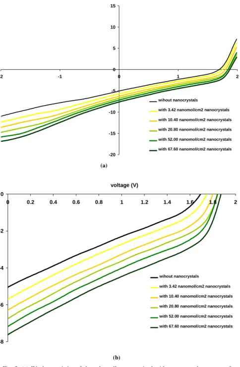
Figure 3(a) shows the current-voltage (IV) characterization of the nanocrystal hybridized Si solar cell under white light illumination, parameterized with respect to the amount of hybridized nanocrystals. Here we use the same green-emitting (CdSe)ZnS nanocrystals for each IV characterization, but vary the amount of hybridized nancrystals for each IV measurement, increasing from a starting total amount of 7.78 nmol (corresponding to a
cross-sectional density of 3.42 nmol/cm2) and reaching a final total amount of 152.10 nmol
(corresponding to a cross-sectional density of 67.60 nmol/cm2). The illumination conditions are all identical in these IV measurements. In this experiment, as the number of nanocrystals hybridized on the solar cell is increased, we observe that the IV curve shifts downwards, indicating that the photocurrent level is increased, given the same input optical beam. The responsivity of the hybridized device seems more or less constant between 240 nm and 280 nm, although the optical absorption of the nanocrystal does not remain constant in this region. In this IV characterization, a xenon light source is deliberately used as the white light illumination source to characterize our solar cells, as also used in Ref. [26], because the UV content provided by this Xe lamp (Newport Corp.) is 7.3% of its full spectrum [36], which is similar to the UV content of the solar spectrum arriving on the earth ground [7]. Here it is worth noting that although the solar simulators are known to be the best in simulating the solar spectrum and its conditions in the visible, they are not apt for characterization in the UV (due to their typical UV content of 3% or less [36]). On the other hand, there are the UV solar simulators specifically designed for UV characterization; but, then these sources are too rich in UV (with a UV content of 35% or more [36]). Therefore, in this work, this Xe lamp serves as one of the best candidates to characterize our solar cells in UV for a solar-like characterization.
-20 -15 -10 -5 0 5 10 15 -2 -1 0 1 2 voltage (V) cu rr e n t ( m A ) wihout nanocrystals
with 3.42 nanomol/cm2 nanocrystals with 10.40 nanomol/cm2 nanocrystals with 20.80 nanomol/cm2 nanocrystals with 52.00 nanomol/cm2 nanocrystals with 67.60 nanomol/cm2 nanocrystals
(a) -8 -6 -4 -2 0 0 0.2 0.4 0.6 0.8 1 1.2 1.4 1.6 1.8 2 voltage (V) c u rre nt ( m A ) wihout nanocrystals
with 3.42 nanomol/cm2 nanocrystals with 10.40 nanomol/cm2 nanocrystals with 20.80 nanomol/cm2 nanocrystals with 52.00 nanomol/cm2 nanocrystals with 67.60 nanomol/cm2 nanocrystals
(b)
Fig. 3. (a) IV characteristics of the solar cell parameterized with respect to the amount of hybridized nanocrystals under Xe white light illumination and (b) IV characteristics of the solar cell zoomed in the 4th quadrant parameterized with respect to the amount of hybridized nanocrystals.
Figure 3 (b) focuses on the IV curves of the solar cells in the 4th quadrant to clearly show the shift of the IV curves with the increasing nanocrystal amount. Here as the number of nanocrystals is increased, we observe that the open circuit voltage and the short circuit current
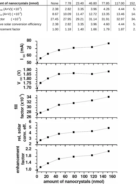
of the solar cell correspondingly increase. This incremental enhancement of the open circuit voltage and the short circuit current with the increments of the hybridized nanocrystals comes from the increasing level of photoemission in the visible. By doing so, more of the otherwise unused UV part of the solar spectrum is converted to the electrical energy, effectively increasing the open circuit voltage and the short circuit current―thus, the fill factor and the solar conversion efficiency. Table 1 summarizes the change of these solar cell parameters.
Table 1. Solar cell parameters change as a function of the nanocrystal amount hybridized on the solar cell. Amount of nanocrystals (nmol) None 7.78 23.40 46.80 77.85 117.00 152.10 (I×V)max (A×V)( ×10
-3 ) 2.38 2.82 3.35 3.96 4.26 4.44 5.01 I sc ×Voc (A×V) ( ×10 -3 ) 8.67 10.09 11.47 12.72 13.35 13.46 14.60 Fill factor ( ×10-2) 27.45 27.95 29.21 31.14 31.91 32.97 34.40 Relative solar conversion efficiency 2.38 2.82 3.35 3.96 4.60 4.44 5.01
Enhancement factor 1.00 1.18 1.40 1.66 1.79 1.87 2.11
Fig. 4. Evolution of (a) short circuit current, (b) open circuit voltage, (c) fill factor, (d) relative solar conversion efficiency, and (e) enhancement factor as a function of the increasing amount of nanocrystals, (a)-(e) in order from the top to the bottom of the figure.
Figures 4(a)–4(e) show evolution of the short circuit current, open circuit voltage, fill factor, relative solar conversion efficiency, and enhancement factor of the solar conversion efficiency as a function of the increasing nanocrystal amount hybridized on the solar cell under Xe white light illumination. When the amount of the nanocrystals is increased to 152.10 nmol, we observe that a maximum enhancement factor of 2.1-folds is achieved with respect to the bare Si solar cell. As the amount of the hybridized nanocrystals is increased more and more, after a certain point we observe that the fitted curve of the enhancement factor converges to a maximum level and we have a diminishing differential enhancement in solar conversion efficiency (see Fig. 4(e)). Although these results are experimentally completely reproducible, some characteristics of the solar cell parameters enhancing incrementally as a function of the nanocrystal amount such as the uneven changes in certain parameters and the incremental enhancement levels are not fully understood. Additional experimental characterization and theoretical modeling is in progress to further understand the scintillation process, the enhancement levels, and the optimization possibilities.
4. Conclusion
In conclusion, for the first time, we reported on a proof-of-concept demonstration of semiconductor nanocrystal based photovoltaic scintillators integrated on solar cells for the enhancement of photovoltaic device parameters including spectral responsivity, open circuit voltage, short circuit current, fill factor, and solar conversion efficiency. Hybridizing (CdSe)ZnS core-shell nanocrystals of 2.4 nm in diameter with a ±5% size distribution on multi-crystalline Si based solar cells, we showed that the spectral responsivity was increased by 10.3 times in the UV range and the solar conversion efficiency was enhanced by 2.1 times under white light illummination similar to the solar spectrum. These experimental results are thought to indicate that such nanocrystal scintillators hold great promise for extending the responsivity of photovoltaic devices towards the ultraviolet region, possibly also presenting commercial value.
Acknowledgment
This work is supported by EU-PHOREMOST Network of Excellence 511616 and Marie Curie European Reintegration Grant MOON 021391 within the 6th European Community Framework Program and TUBITAK under the Project No. 106E020, 107E088, 107E297, 104E114, 105E065, and 105E066. Also, HVD acknowledges additional support from the Turkish Academy of Sciences Distinguished Young Scientist Award (TUBA GEBIP) and European Science Foundation (ESF) European Young Investigator Award (EURYI) Programs. IMS acknowledges TUBITAK Graduate Fellowship Program. The authors are also pleased to acknowledge using the facilities of Bilkent University Nanotechnology Research Center (Founder Prof. E. Ozbay) and Advanced Research Laboratories and Institute of Materials Science and Nanotechnology (Founder Prof. S. Ciraci). The authors would further like to thank Dr. N. Kosku Perkgoz, Dr. A. Dana, and Dr. M. Gokkavas for useful discussions.