PROCEEDINGS OF SPIE
SPIEDigitalLibrary.org/conference-proceedings-of-spie
Low dark current diffusion limited
planar type InGaAs photodetectors
Dolas, M. Halit, Atesal, Okan, Caliskan, M. Deniz, Bek,
Alpan, Ozbay, Ekmel
M. Halit Dolas, Okan Atesal, M. Deniz Caliskan, Alpan Bek, Ekmel Ozbay,
"Low dark current diffusion limited planar type InGaAs photodetectors," Proc.
SPIE 11129, Infrared Sensors, Devices, and Applications IX, 111290D (9
September 2019); doi: 10.1117/12.2528666
Event: SPIE Optical Engineering + Applications, 2019, San Diego, California,
United States
Low Dark Current Diffusion Limited Planar Type InGaAs
Photodetectors
M. Halit Dolas
*a, b, Okan Atesal
a, M. Deniz Caliskan
a, Alpan Bek
b, Ekmel Ozbay
aa
Nanotechnology Research Center (NANOTAM)
Bilkent University, Ankara, Turkey
b
Micro and Nanotechnology Department
Middle East Technical University, Ankara, Turkey
ABSTRACT
In this work, we design and produce 1280x1024 format InGaAs based planar type detectors with 15µm pixel pitch. We have obtained diffusion current limited low dark current (~10fA) and high responsivity (1.08A/W at 1.55µm) values at room temperature conditions. Moreover, dark current modeling is performed using diffusion, generation & recombination (GR) and trap assisted tunneling (TAT) current mechanisms. Ideality factor is extracted from forward bias characteristics. Excellent match between modeling and experimental data is reached. Also, temperature dependency of dark current is studied in 10oC – 60oC ranges. The area and perimeter related dark current components are differentiated using test detectors with changing diameters that are placed next to the detector array structure. Experimental data shows good agreement with theoretical expectations.
Keywords: SWIR, InGaAs, Planar p-n diodes, Low dark current, Megapixel
1. INTRODUCTION
Imaging technology in Short Wavelength Infrared (SWIR) band is employed in many applications from military, industrial and medical fields1. Among the great number of its critical properties, one of the most accentuated ability of SWIR imaging is passive night vision by making use of the night glow under even moonless night conditions2. However, this feature requires very low dark current values that enable to operate at low noise detection regime. Lattice matched InGaAs/InP based planar type photodetectors are the most appropriate candidate for this purpose3. For this material system, low dark current values can be possible with planar type processing4-8 for which, low bandgap InGaAs absorber layer remains buried under high bandgap InP layer that significantly limits the surface current which is the main problem in mesa type processing. Further dark current reduction is also possible by optimizing epitaxial layer’s doping values and junction placement with an acceptably low decrease in photo responsivity.
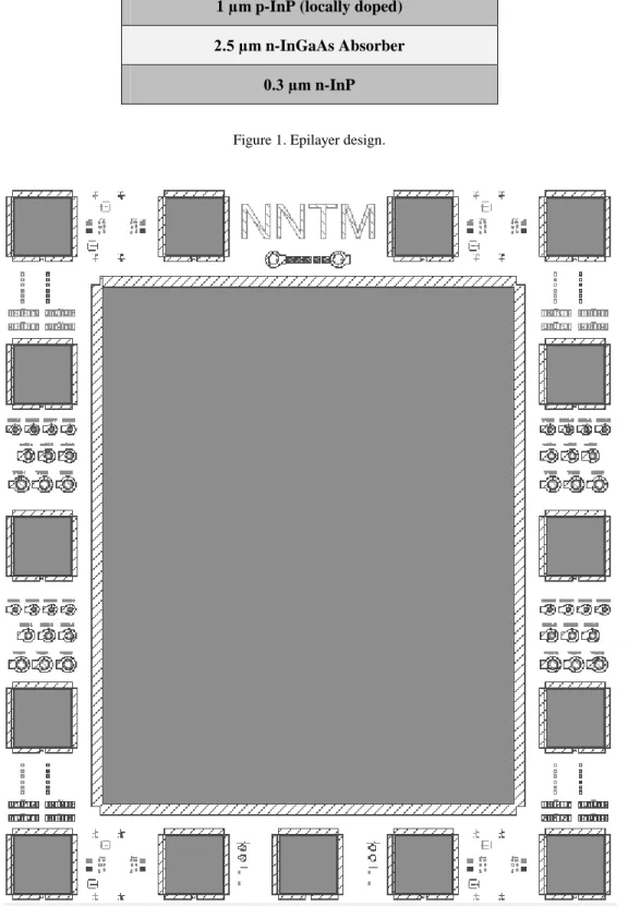
From top to bottom, our epitaxial design contains 0.2 µm thick InGaAs cap layer that provides ohmic p-contacts for each pixel, 1 µm thick top InP layer that is locally p type doped after crystal growth to complete p-i-n structure and pixel isolation, 2.5 µm thick InGaAs absorber layer and 0.3 µm thick common n-contact bottom InP layer as illustrated in Fig. 1. Mask layout design that is used in experimental work is also given in Fig. 2. It contains a 1280x1024 format focal plane array (FPA) at the middle. Test structures that contain single standing pixels with 100, 200 and 300 µm active diameters, test pixel arrays in 150x150 formats that have exactly the same design with the FPA as they include shortened 10x10 pixel groups to be able to eliminate electronic noise from measurement setup during estimation of a single FPA pixel dark current, wide active area single standing pixels for responsivity measurement and alignment marks that is used to align different lithography steps are placed around FPA. For the FPA and the small format test pixel arrays, common contact region is placed as it frames the pixel area from all 4-sides. Electrical and optical characterizations are realized using above mentioned test structures in order not to harm the FPA during measurements.
* Corresponding author: [email protected] ; Phone: +90 312 290 1966 ; Fax: +90 312 266 4042
Infrared Sensors, Devices, and Applications IX, edited by Paul D. LeVan, Priyalal Wijewarnasuriya, Ashok K. Sood, Proc. of SPIE Vol. 11129, 111290D
© 2019 SPIE · CCC code: 0277-786X/19/$18 · doi: 10.1117/12.2528666
InGaAs Cap Layer 1 µm p-InP (locally doped) 2.5 µm n-InGaAs Absorber
0.3 µm n-InP Figure 1. Epilayer design.
Figure 2. Mask Layout
Cleanroom process starts with PECVD SiNx coating on top. ICP-RIE is used to create diffusion openings and alignment
marks. Zn3P4 and SiNx top coatings are realized together in the same chamber by thermal evaporation and sputtering
respectively. High temperature diffusion oven is used to drive Zn atoms through the diffusion openings to create p type doped regions. HF:HNO3 (1:1) acid solution is used to clean SiNx and Zn3P4 coatings after diffusion. Ti/Au p-contacts
are coated by thermal evaporation and liftoff technique. 3-step chemical etching, which is designed creating a ladder-like shape to ensure metal continuity during n-contact coating, used to reach buried bottom InP layer. H3PO4:H2O2:H2O
(1:1:3) and HCl:H3PO4 (1:3) acid solutions that are selective etchants for InGaAs and InP layers used in chemical
etching. Ti/Au n-contacts are coated by thermal evaporation and liftoff technique. For FPA, n-contact metal is coated on the bottom InP layer as it continue through ladder-like shaped region to reach the same level with p-contacts. This leveling has a critical role in indium bump bonding process for which the n and p indium bumps need to be at the same height. InGaAs cap layer is etched in the area between pixels for isolation and spin-on benzocyclobutene (BCB) passivation layer is coated on top. ICP-RIE is used for passivation opening and Ti/Ni/Au/In is coated by thermal evaporation and liftoff technique on the opened areas. Backside of the FPA is mechanically cleaned with grinding and an anti-reflection layer consists of TiO2 and SiO2 is sputtered on the cleaned surface. After dicing, FPA is bonded to an
appropriate silicon read-out integrated circuit (ROIC) chip, which is also coated with Ti/Ni/Au/In on top of each pixel, by FC150 flip-chip bonder.
All IV measurements are realized in a light-proof room that is designed as a faraday cage. B1500 semiconductor analyzer connected to a probe station is used to collect data from the test structures. Photo current measurements are conducted with employing 1.55 µm laser source coupled to an infrared fiber. Optical power at the end of the fiber is measured in terms of Watts. Test pixel is illuminated with fiber from backside and the change in current is measured in terms of Amperes. Based on the measurement, responsivity value in terms of A/W is directly estimated which provides a reliable result.
2. RESULTS AND DISCUSSION
Dark current measurements of differently sized pixels at room temperature (~25 ⁰C) are given in Fig. 3a. FPA pixel dark current data is measured from 10x10 pixel group in a test structure and proportionated to a single pixel. Fig. 3b shows photo current measurement from wide area test pixel. Responsivity is estimated as 1.08 A/W, which corresponds %86 quantum efficiency for 1.55 µm.
Figure 3. a) Dark current measurements of differently sized pixels. b) Photo current measurement.
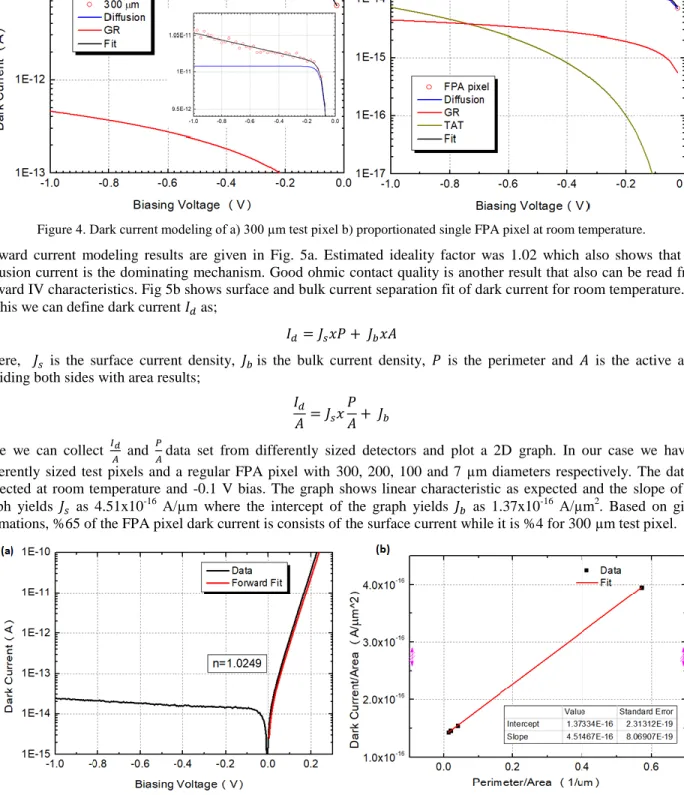
Dark current modeling is realized by considering voltage dependencies of diffusion, GR and TAT mechanisms. Fig. 4a shows room temperature data from 300 µm test pixel. Diffusion current is found as the dominating mechanism. The small difference between total current and diffusion current is showed is smaller graph inside Fig. 3a. GR current was not effective comparing with diffusion current, and TAT current was extremely small as it is excluded. Fig 4b shows dark current modeling of a proportionated single FPA pixel at room temperature. As the surface of the device become more important, surface depended portion of GR and TAT mechanisms reached higher values. However, near working
bias region (0.1-0.3 V) diffusion current was still the dominating mechanism as it is more than 5 times higher than the others. In each modeling work, excellent match between experimental data and theoretical model is reached.
Figure 4. Dark current modeling of a) 300 µm test pixel b) proportionated single FPA pixel at room temperature.
Forward current modeling results are given in Fig. 5a. Estimated ideality factor was 1.02 which also shows that the diffusion current is the dominating mechanism. Good ohmic contact quality is another result that also can be read from forward IV characteristics. Fig 5b shows surface and bulk current separation fit of dark current for room temperature. To do this we can define dark current as;
Where, is the surface current density, is the bulk current density, is the perimeter and is the active area. Dividing both sides with area results;
Here we can collect and data set from differently sized detectors and plot a 2D graph. In our case we have 3 differently sized test pixels and a regular FPA pixel with 300, 200, 100 and 7 µm diameters respectively. The data is collected at room temperature and -0.1 V bias. The graph shows linear characteristic as expected and the slope of the graph yields as 4.51x10⁻¹⁶ A/µm where the intercept of the graph yields as 1.37x10⁻¹⁶ A/µm2. Based on given estimations, %65 of the FPA pixel dark current is consists of the surface current while it is %4 for 300 µm test pixel.
Figure 5. a) Forward dark current modeling b) separation of surface and bulk dark current components.
Temperature dependent IV characteristics of FPA pixel is measured in between 10-60 ⁰C with 2 ⁰C intervals as given in Fig. 6a. Diffusion current domination is increasing for higher temperatures since the temperature dependency of diffusion current is higher than the GR and TAT current. This leads to a flattening of IV curve. Total dark current is estimated 1nA/cm2 at 10 ⁰C which is the planned working point of the final camera. Fig. 6b shows the room temperature dynamic resistance curve. To reduce the Johnson-Nyquist noise (thermal noise), bias point should be chosen as it maximizes dynamic resistance. In our case, -0.3V found as an optimum biasing point.
Figure 6. a) Temperature depended IV characteristics of FPA pixel b) room temperature dynamic resistance curve
A camera scene of the final product is given in Fig.7. 2 point non-uniformity correction and a basic median filter are applied to the raw image. Small dead pixel clusters are caused from unwanted BCB openings during hard cure that will be optimized further in future works.
Figure 7. a) A camera scene using developed detector. (M. Halit Dolas (left), Okan Atesal (right))
3. CONCLUSION
We successfully designed a SWIR InGaAs/InP based heterojunction p-i-n detector with 1nA/cm2 total dark current density at 10 ⁰C and %86 quantum efficiency at 1.55 µm. Both reverse and forward IV characterizations show that dark current is dominated by diffusion current which is the ideal p-n junction dark current mechanism. Surface and bulk current components are separated and for FPA pixels it is found that %65 of the dark current comes from the surface current. Therefore, further dark current decrease would be possible with different passivation materials which will be our future work. For current detectors, -0.3V which maximizes dynamic resistance found as an optimum working bias to obtain minimum Johnson-Nyquist noise.
REFERENCES
[1] Hansen, Marc P., and Douglas S. Malchow. "Overview of SWIR detectors, cameras, and applications." SPIE
Defense and Security Symposium. International Society for Optics and Photonics, (2008).
[2] Yuan, Henry, et al. "Low dark current small pixel large format InGaAs 2D photodetector array development at Teledyne Judson Technologies." SPIE Defense, Security, and Sensing. International Society for Optics and Photonics, (2012).
[3] Verdun, Michael, Gregoire Beaudoin, Benjamin Portier, Nathalie Bardou, Christophe Dupuis, Isabelle Sagnes, Riad Haidar, Fabrice Pardo and Jean-Luc Pelouard. "Dark current investigation in thin PiN InGaAs photodiodes for nano-resonators." Journal of Applied Physics, vol. 120, no. 8, (2016).
[4] Yuan, Henry, Mike Meixell, Jiawen Zhang, Philip Bey, Joe Kimchi, Louis C. Kilmer. "Low dark current small pixel large format InGaAs 2D photodetector array development at Teledyne Judson Technologies." SPIE Defense, Security, and Sensing. International Society for Optics and Photonics, May (2012).
[5] Onat, Bora M., Wei Huang, Navneet Masaun, Michael Lange, Martin H. Ettenberg, Christopher Dries. "Ultra-low dark current InGaAs technology for focal plane arrays for "Ultra-low-light level visible-shortwave infrared imaging." Defense and Security Symposium. International Society for Optics and Photonics, May (2007). [6] Acton, David, Michael Jack, and Todd Sessler. "Large format short-wave infrared (SWIR) focal plane array
(FPA) with extremely low noise and high dynamic range." SPIE Defense, Security, and Sensing. International Society for Optics and Photonics, May (2009).
[7] MacDougal, Michael, Andrew Hood, Jon Geske, Jim Wang, Falgun Patel, David Follman, Juan Manzo, Jonathan Getty. "InGaAs focal plane arrays for low-light-level SWIR imaging." SPIE Defense, Security, and Sensing. International Society for Optics and Photonics, May (2011).
[8] Fraenkel, R., et al. "Development of low-SWaP and low-noise InGaAs detectors." Infrared Technology and Applications XLIII. Vol. 10177. International Society for Optics and Photonics, (2017).