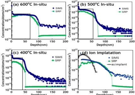
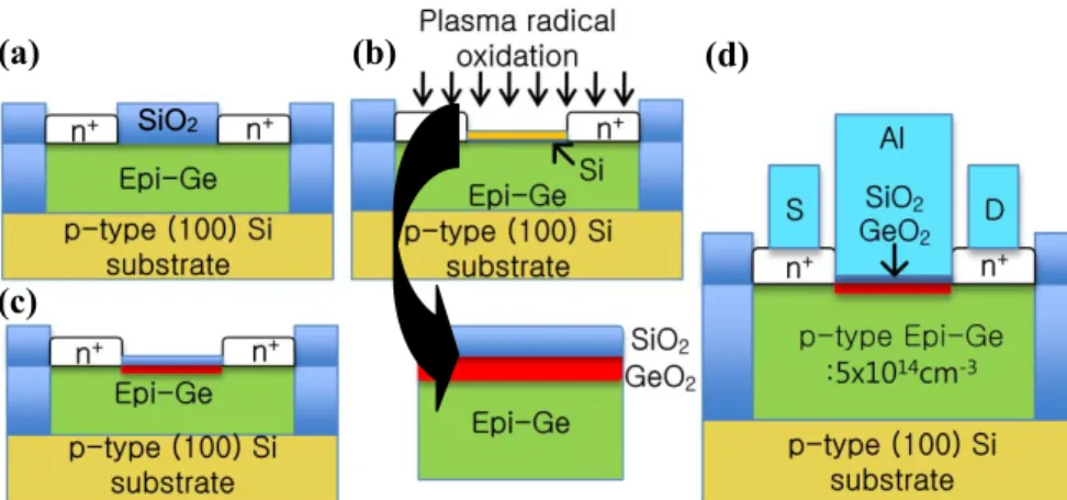
High performance n-MOSFETs with novel source/drain on selectively grown Ge on Si for monolithic integration
Tam metin
Şekil
Benzer Belgeler
In this new classification problem, each association rule R is seen as a query instance whose target feature value (which is either interest- ing or uninteresting) is unknown and
conjugated polymers are on their way to earning an irreplaceable position for use in white light generation though phosphors have thus far been most extensively used for white
The holograms of the micro-lenses are recorded in the near infrared by means of digital holographic microscopy as image -plane holograms whereas the holographic
From the 1950s, egg production systems of laying hens have undergone remarkable changes which have affected hen behaviour and welfare such as feather pecking,
Samvel ¡an Translation of the Predicative Element of a Sentence: Category Switching, Aspect and Diathesis Proceedings of the Fourth International Conference on
The two previous efforts for automatic self-reported pain mea- surement required an intermediate learning stage (i.e., two-step approaches). They first predicted the PSPI or the VAS
The purpose of this paper is to discuss the evaluation of dif- ferent alternatives for the implementation of Turkish army corps artillery ammunition supply system. The objective is
In addition, the Chern number map for the phase space indicates that the region corresponding to the triangular lattice is found to roughly follow the centered rectangular
