MICROFLUIDICS FOR PLASMONIC SENSORS
A THESIS
SUBMITTED TO THE GRADUATE PROGRAM OF MATERIALS SCIENCE AND NANOTECHNOLOGY
AND THE INSTITUTE OF ENGINEERING AND SCIENCES OF BILKENT UNIVERSITY
IN PARTIAL FULLFILMENT OF THE REQUIREMENTS FOR THE DEGREE OF
MASTER OF SCIENCE
By
Yavuz Nuri Ertaş September 2009
i I certify that I have read this thesis and that in my opinion it is fully adequate, in
scope and in quality, as a thesis for the degree of Master of Science.
Assist. Prof. Dr. Mehmet Bayındır (Supervisor)
I certify that I have read this thesis and that in my opinion it is fully adequate, in scope and in quality, as a thesis for the degree of Master of Science.
Assist. Prof. Dr. Ali Kemal Okyay
I certify that I have read this thesis and that in my opinion it is fully adequate, in scope and in quality, as a thesis for the degree of Master of Science.
Prof. Dr. Salim Çıracı
Approved for the Institute of Engineering and Sciences:
Prof. Dr. Mehmet B. Baray
ii
ABSTRACT
MICROFLUIDICS FOR PLASMONIC SENSORS
Yavuz Nuri ErtaşM.S. in Graduate Program of Materials Science and Nanotechnology Supervisor: Assist. Prof. Dr. Mehmet Bayındır
September 2009
In this thesis, we integrate microfluidics with grating-coupled surface plasmon configurations for sensing applications. First, in order to observe optimal excitations, we introduce procedures for modification of the surface profiles of gratings acquired from commercially available optical storage disks. A must requirement in plasmonic systems, thin film metal deposition is performed. Soft lithographic techniques are applied to coated disks to transfer the surface topography of the disks to an elastomeric material, PDMS. Optical lithography is used to fabricate microfluidic channels to where fluid will be injected. After fabricating the final structure, ellipsometric measurement is used to investigate the device performance. Experimental results were in consistence with the theoretical simulations providing similar behaviours of reflection spectra. The resonance wavelengths are found to be occuring very near to the expected values along with high quality factors. However, to the device structure, an intensity loss is observed which can be further improved. We achieved the tuning of the resonance wavelength by changing the refractive index of the medium inside the microchannel. Integration of the microfluidic channel to surface plasmon studies may open up many applications such as biomolecular sensing.
iii
ÖZET
PLAZMONİK SENSÖRLER İÇİN MİKROAKIŞKANLAR
Yavuz Nuri ErtaşMalzeme Bilimi ve Nanoteknolji Yüksek Lisans Programı Yüksek Lisans
Tez Yöneticisi: Yar. Doç. Dr. Mehmet Bayındır
Eylül 2009
Bu çalışmada, mikroakışkan kanalların plazmonik sistemlerle entegrasyonu gösterilmiştir. Öncelikle, yüzey plazmonlarının en etkili bir şekilde uyarımı için optik disklerin yüzeylerindeki kırınım ağı yapısı çeşitli fiziksel be kimyasal prosedürlere tabi tutularak modifiye edilmiştir. Plazmonik sistemlerin hemen hepsinde gerekli olan ince metal tabaka kaplaması yapıldıktan sonra kalıplama litografisi kullanılarak optik disklerin yüzey profilleri, elastomerik bir malzeme olan PDMS’e aktarılmıştır. Çeşitli sıvıların enjekte edileceği mikroakışkan kanalların fabrikasyonu içinse optik litografi tekniği kullanılmıştır. Çeşitli teknikler kullanılarak sonhaline gelen PDMS’ten oluşan yapının performans ölçümleri için elipsometre cihazı kullanılmıştır. Deneysel veriler ile teorik simule edilenlerin tutarlı olduğu görülmüştür. Yansıyan sinyal genliğinde bir düşüş gözlenmiş olsa da rezonans dalgaboyları, simule edildiği üzere beklenen değerlere oldukça yakın çıkmıştır. Farklı sıvılar kullanılarak yapılan ölçümlerde beklendiği üzere rezonans kaymaları görülmüştür. Sonuç olarak mikrokanalların plazmonik tabanlı uygulamalarda kullanılması daha da geliştirilerek, biyomoleküler detekte işlemleri gibi bazı önemli uygulamalar için avantajlı bir alternatif olacaktır.
iv
ACKNOWLEDGMENTS
It would be very selfish to say that this thesis has been the product of my efforts only. Many people have contributed to its completion in many ways: spiritual, psychological, scientific, financial and technical.
First and foremost, I offer my gratitude to my supervisor Mehmet Bayındır. Besides my advisor, I would like to thank the rest of my thesis committee: Prof. Ali Kemal Okyay and Prof. Salim Çıracı for their insightful comments and hard questions.
In addition, a thank you goes to Prof. Aykutlu Dȃna for his encouragement and providing practical fabrication techniques without losing his modesty for a moment.
I thank my fellow groupmates in Bayındır Research Group: Dr. Mecit Yaman Dr. Abdullah Tülek, Dr. Hakan Deniz, Murat Kılınç, Kemal Gürel, Mert Vural, Adem Yildirim, H. Esat Kondakçı, Erol Özgür, Tural Hudiyev, Mehmet Kanik, Özlem Köylü, Duygu Akbulut, Hülya Budunoğlu, Özlem Şenlik, Ahmet Ünal, Can Koral, Tarık Çeber, Ekin Özge Özgür, Yunus Çetin, Muhammed Çelebi, Y. Emre Akbaş, M. Halit Dolaş and Serkan Kasırga.
I also would like to thank UNAM engineers; Burkan Kaplan, Mustafa Güler, Koray Mızrak and Emre Tanır.
I appreciate the motivation, technical help and moral support of my precious friends Hasan Güner and Mustafa Ürel.
Very special thanks goes to Sencer Ayas for his endless support in every aspect one can imagine. Meeting him was a real privilege for me even more valuable than completing this thesis.
v
Table of Contents
1 Introduction and Motivation ... 1
2 Theoretical Background ... 6
2.1 Surface Plasmons ... 6
2.2 Electromagnetic waves at interfaces ... 7
2.3 The dielectric function of a metal ... 9
2.4 Surface Plasmons at a Metal-Dielectric Interface ... 12
2.5 Excitation of Surface Plasmons... 18
2.5.1 Prism Coupling ... 19
2.5.2 Grating Coupling ... 23
3 Simulations ... 27
3.1 Angular Interrogation Simulations... 29
3.2 Wavelength Interrogation Simulations... 32
4 Fabrication and Characterization ... 38
4.1 Fabrication and Characterization of Gratings ... 38
4.1.1 DVDs as a Grating Source... 38 4.1.2 Soft Lithography ... 45 4.1.3 Metal Deposition ... 49 4.1.4 Optical Lithography ... 51 4.1.5 Plasma Oxidation ... 53 5 Measure ments... 55 6 Conclusions ...60
vi
List of Figures
Figure 1.1 Typical setup for a SPR biosensor Adopted from Ref. [12 ]...4
Figure 2.1 Electric field lines of a surface plasmon on a smooth surface...6
Figure 2.2 An electromagnetic wave at an interface ...8
Figure 2.3 Geometry for wave propagation at a metal-dielectric interface ...13
Figure 2.4 Dispersion curves and photonic light lines for air and silica ...18
Figure 2.5 Dispersion relation for prism couling. ...20
Figure 2.6 Otto configuration for prism couling. ...21
Figure 2.7 Kretschmann configuration for prism coupling ...21
Figure 2.8 Reflectivity for prism coupling with Kretschmann geometry ...22
Figure 2.9 Grating coupling configuration. ...24
Figure 2.10 Multiple dips in reflectivity for grating coupling configuration...25
Figure 2.11 The plasmonic dispersion relation for grating coupling ...25
Figure 3.1 Simulated Structure ...28
Figure 3.2 Reflection spectrum with respect to incident angle when air is used as the dielectric layer ...29
Figure 3.3 Reflection spectrum with respect to incident angle when water is used as the dielectric layer. ...30
Figure 3.4 Reflection spectrum with respect to incident angle when 0.9% NaCl solution is used as the dielectric layer. ...30
Figure 3.5 Reflection spectrum with respect to incident angle when isopropanol is used as the dielectric layer. ...31
Figure 3.6 Reflection spectrum with respect to incident angle for all the simulated materials ...31
Figure 3.7 Reflection spectrum with respect to incident angle when air is used as the dielectric layer. ...34
vii
Figure 3.8 Reflection spectrum with respect to wavelength when water is used as
the dielectric layer. ...35
Figure 3.9 Reflection spectrum with respect to wavelength when 0.9% NaCl solution is used as the dielectric layer. ...35
Figure 3.10 Reflection spectrum with respect to wavelength when isopropanol is used as the dielectric layer. ...36
Figure 3.11 Reflection spectrum with respect to wavelength for all the simulated materials ...36
Figure 4.1 DVD handling process...39
Figure 4.2 Profiles of the gratings on a DVD-R disk for various etching times...40
Figure 4.3 Surface topography and line profile of etched disks ...41
Figure 4.4 Procedure for surface modification of the disks ...42
Figure 4.5 Thickness variation with spin speed for 950K PMMA A2, in Anisol 43 Figure 4.6 Surface topography and line profile of the disk having metal coating on it...44
Figure 4.7 Surface topography and line profile of the PMMA spinned disk ...45
Figure 4.8 PDMS molded disc manipulation ...47
Figure 4.9 PDMS molding steps from a master ...47
Figure 4.10 Surface topography and line profile of the PDMS mold. ...48
Figure 4.11 Metal coating process ...49
Figure 4.12 Surface topography and line profile of silver coated PDMS mold ....50
Figure 4.13 Schematic representation of the fabrication process of a microchannel ...52
Figure 4.14 Fabricated microchannel images on a glass and a PDMS mold ...53
Figure 4.15 Chemical structure of PDMS...54
Figure 4.16 Demonstration of the final form of the fabricated structure ...54
Figure 5.1 Measured reflection spectrum with respect to wavelength when air is used as the dielectric layer ...56
viii
Figure 5.2 Measured reflection spectrum with respect to wavelength when water
is used as the dielectric layer ...56
Figure 5.3 Measured reflection spectrum with respect to wavelength when 0.9%
NaCl solution is used as the dielectric layer ...57
Figure 5.4 Measured reflection spectrum with respect to wavelength when
isopropanol is used as the dielectric layer ...57
Figure 5.5 Measured reflection spectrum with respect to wavelength for all the
measured dielectric materials ...58
Figure 5.6 Comparison of theoretical and experimental results for different
dielectric materials ...58
Figure 5.7 Fluid injection into microchannel while the PMMA structure is
attached to the ellipsometer sample holder ...59
1
CHAPTER 1
INTRODUCTION & MOTIVATION
Over the last two decades, we have witnessed notable research and development activity aimed at the realization of optical sensors for the measurement of physical, chemical and biological quantities. Optical sensors that are based on excitation of surface plasmons, generally referred to as surface plasmon resonance (SPR) sensors, belong to the set of refractometric sensing devices. These devices include resonant mirror sensor, the grating coupler sensor, the integrated Young interferometer, the integrated optical Mach- Zehnder interferometer and the white light interferometer which measure changes in the refractive index occurring in the field of an electromagnetic wave supported by the optical structure of the sensor [1,2]. Although having alternatives, SPR sensors, due to their several unique advantages, has been receiving remarkable attention from scientific and industrial environments. The applications of this technique have a short history but many commercial products are already available in the market. Even though much of this success has been new, SPR fundamentals have long played an important role in surface sciences. In the beginning of the 20th century, the excitation of surface plasmons, described as Wood’s Anomalies, was observed as unusual reflective patterns when polarized light was introduced on a metal grating. In this phenomenon, photons of the polarized light resonantly couple to the oscillation of metal- free electrons. This generates a strong electromagnetic evanescent wave bound to the metal surface [3].
2 Later, scientists began to consider surface plasmon resonance technique for practical purposes. First studies were made on characterization of thin films and detecting processes at metal interfaces in the late 1970s. Since the initial demonstration of surface plasmon resonance for the study of processes at the surfaces of metals and sensing of gases in the early 1980s, SPR sensors have made vast advances in terms of both development of the technology and its applications. In 1982, the use of SPR for gas detection and biosensing was demonstrated by Nylander and Liedberg [4,5]. Since then SPR sensing has been receiving continuously rising interest from scientific community. In 1988, Rothenhausler and Knoll showed surface plasmon microscopy for the firs t time for imaging applications [6]. So far, new configurations for SPR-sensing devices were demonstrated and also many applications for the measurement of physical, chemical and biological entities have been described. Also, SPR biosensors have become a central tool for determining and characterizing the biomolecular interactions since it provides rich information on the specifity, affinity and kinetics of biomolecular interactions. More than %75 of SPR applications reported in the literature focus on biomolecular interactions. The reason for this conspicuous statistics comes from the SPR’s being capable of providing real time and label- free measurements along with its surface oriented method nature. Moreover, development of SPR sensors for detection of chemical and biological species has gained considerable momentum and the number of publications reporting applications of these sensors has been rapidly growing [1,2].
The underlying reasons behind the popularity of surface plasmon resonance (SPR) spectroscopy can be summarized as SPR sensor’s label- free, rapid, real-time, highly sensitive and high- throughput measurement opportunities. Current trends in this technology are directed toward providing an integrated, low-cost, reusable and sensitive biosensor along with further miniaturization of the sensing system and extending the platform to high-throughput capabilities. In order to realize these, lowering the scale of the sensing chips and their integration into microfluidic devices that will open the way for large parallel operations are required. Even though much more progress is needed, SPR sensor technology has already been commercialized by several companies such as Biacore, Sensata,
3 Reichert, Nomadics and Pittcon. In the near future, one can foresee that SPR technology will continue gaining its popularity among researchers resulting in more research studies and scientific information accumulation that will pave the way for appearance of new products on the market [1,7].
On the other hand, in recent years, considerable progress has been made in the field of miniaturization. It is now effectively possible to miniaturize all kinds of systems such as mechanical, fluidic, electromechanical and thermal. This miniaturization gave birth to microfluidics in the 1990s. It did not take many years for microfluidics to become a widely studied fie ld. The use of microfluidic systems has shown great promise for many applications including biomedical research, chemical analysis, biological analysis and microelectronics. In all kinds of microfluidic systems, a detection method that can quickly and sens itively monitor analytes in the microfluidic channels is an essential requirement. Often, indicators, also known as labels, are attached to a sample analyte before experiment to report the presence and movement of the analyte. Label-based detection techniques have played a significant role in the development of microfluidic devices but generally they require extra sample preparation steps and the attachment of labels may alter the native functions of the sample molecules. Due to these drawbacks, a label- free method is highly desired for microfluidics and sensors applications. At this point the integration of surface plasmon resonance technique with the microfluidics plays a crucial role since SPR is as a powerful label- free analysis technique. The combination of a microfluidic device with SPR offers three major advantages. (1) Flow channels with nanolitre volumes are provided by microfluidic devices. This causes surface binding events occur faster because the reagents are quickly replenished by the liquid flo w. (2) Less sample consumption is provided by the use of microfluidics. (3) Detection region of SPR technique is on the order of several square centimetres. For high throughput operations, the functional components in the microfluidic device may be copied in parallel. Furthermore, a microfluidic device is well-suited for automation, which allows sequenced and computer controlled manipulations for the efficiency and precision of surface binding events [8,9].
4 Figure 1.1: Typical setup for a SRP biosensor (Adapted from [12]).
Combining microfluidics with SPR technology is a novel idea that has started in early 2000s. In 2001, Lee et al. utilized microfluidic channels in SPR imaging experiments for the detection of DNA and RNA adsorption onto chemically modified gold surfaces. They were able to monitor DNA-DNA, DNA-RNA and protein-DNA interactions down to nanomolar concentrations [10]. Almost all biosensor applications of surface plasmon resonance systems require a sensing environment. As shown in Figure 1.1, a microfluidic channel is generally used to maintain a medium for molecular interactions. Here, the channel surface is functionalized in order to monitor the key-lock events. In 2004, Wheeler et al. proposed rapid and a simple fabrication method and demonstrated a device for detection of sequential layers of protein binding [11].
Later in 2008, Luo et al. designed and fabricated a microfluidic device containing an array of gold spots onto which antigens and antibodies of interest
5 can be attached. They used SPR imaging to monitor the antibody-antigen recognition and binding events. The researchers reported that the sensitivities on the order of picomolar levels were obtained [9]. Recently, Zhang et al. showed a new type of low cost disposable polymeric sensor chip based on grating coupling of surface plasmon modes combined with a microfluidic channel system. They monitored the self- assembly of a monomolecular film (SAM), a thiol derivative, onto the Au surface of the sensor chip. In order to adsorb the mercapto-terminated polyethylene glycol (mercapto-PEG), a phosphate-buffered saline (PBS) solution that contained mercapto-PEG was introduced to the functionalized gold surface. SPR measurements indicated the formation of the PEG SAM on the Au surface. As a result, combination of the polymeric microfluidic sensor fabrication techniques with the functionalization of the surfaces and surface plasmon resonance technique was demonstrated [7].
6
CHAPTER 2
THEORETICAL BACKGROUND
2.1 Surface Plasmons
Surface plasmons are propagating charge density oscillations of the metal free electrons occuring at the interface shared with a dielectric. They can also be considered as strongly bound electromagnetic waves to the interface. In order to generate surface plasmons, presence of free electrons at the interface of two materials is needed. This always suggests that one of the media is metal which provides plentiful free conduction electrons.
7 An electromagnetic field occurs when the surface charge density changes dynamically (Figure 2.1). Closer to the surface, the field shows a strong enhancement due to the resonant response of oscillating electrons. This field decays exponentially into both media. Surface plasmons can be excited by electrons and photons. This excitation occurs as the electrons’ collectively and in resonance response to a photon or electron. In the case electrons are used for excitation, as the electrons scatter from the metal, energy is transferred into the plasma. The parallel component of the scattering vector to the metal-dielectric interface brings the formation of a surface plasmon. Excitation by means of photons requires an additional medium such as prism or grating structure in order to match the wave vectors of the incoming photon and surface plasmon.
2.2 Electromagnetic waves at interfaces
Consider two materials share a common flat interface at z = 0 as shown in Figure 2.2. Let’s define the electromagnetic response of each material i with a dielectric function εi and with a refractice indice ni. If we define angle of incidence with αi and angle of transmission αt , Snell’s law of refraction can be written as follows:
(2.1)
When αr = - αi , reflection occurs. For n1 > n2 , αt is always larger than αi. If αr = 90o, the incoming wave is completely reflected and no transmission of light into the second medium is observed. This phenomenon is known as total internal reflection (TIR). When TIR condition is satisfied, the angle of incidence is called as the critical angle and is given by:
8 Figure 2.2: An electromagnetic wave at an interface.
It is seen that Ei is divided into two components at the interface which are reflected wave Er and transmitted wave Et. Here, it should be questioned that how does the coming intensity separate between two components. Fresnel solved this problem by using the continuity conditions for the tangetial components of E and H. If its wavevector is situated within the xz - plane, any arbitrary plane electric field can be decomposed into a component that is lying within the xz - plane and an orthogonal component that acts parallel to the y - axis. When E is perpendicular to the plane of incidence, that is, the xz – plane, the case could be defined as transverse electric field (TE mode) or s - polarization. Also it is called transverse magnetic field (TM mode) or p - polarization if E is everywhere parallel to the plane of incidence. Fresnel’s formulas express the ratio of the electric field amplitude of the reflected (or transmitted) wave divided by the incident wave amplitude for the two polarizations:
9
Reflected light for s - polarization
Transmitted light for s - polarization
Reflected light for p – polarization (2.3)
Transmitted light for s – polarization
2.3 The Dielectric Function of a Metal
Plasma model is frequently used to explain the optical properties of metals. In this model, valence electrons of the metal are assumed to be completely detached from their ions which form a free electron gas. The free electron model of metals is attributed to Paul Drude and is known to be simplest way to represent the electronic structure of metals [13]. Although Drude model is an oversimplification of the reality, amazingly it works quite good between visible and microwave regime. According to this model, the valence electrons of the metal become conduction electrons and travel freely. The electron – electron interactions are neglected in Drude model however ion – electron interactions can not be fully ignored which is named as quasi–free electron approximation. The model says that the band structure properties are based on the effective optical mass m of each electron.
The response of a metal to an externally applied electric field is basically determined by the acceleration forced upon the electrons. Electrons experience
10 mutual collisions with each other after time intervals equal to the collision time τ. The oscillatory motion of the electrons damp with a collision frequency of γ = 1 /
τ. Collision time τ is also known as relaxation time of free electron gas.
In order to derive plasma frequency and dielectric function, we begin by considering the oscillations of a free electron under an external electric field. The equation of motion for the displacement x of the electron is:
(2.4)
The first term corresponds to the acceleration of the electron, while the second is the frictional damping force of the medium. The term on the right hand side is the driving force applied by the light. Applied electromagnetic field is assumed to be harmonic time dependent in the form E(t) = E0e-iωt where ω is the frequency of the light. Then the solution is assumed in the form of x(t) = x0e-iωt . By substituting E(t) and x(t) into Equation 2.4, we obtain
(2.5)
The polarization P of the gas is equal to P = – nex, where n is the number of the electrons per unit volume. Then P becomes
(2.6)
Inserting Equation 2.6 into D = ε0E + P gives
11 where is the square of the plasma freq uency of the free electron gas. Finally, the dielectric function of the free electron gas can be written as
(2.8)
The real and complex parts of the dielectric function ε(ω) = ε1(ω) + iε2(ω) are found as follows
(2.9)
(
2.10)When frequecies close to ωp is employed, ωτ >> 1 is obtained and also ε2(ω) is considered as negligible resulting to a real dielectric constant of
(2.11)
Interband transitions does not allow Equation 2.11 valid for noble metals since ε2 can no longer be disregarded. For low frequencies, ωτ << 1, the imaginary part of the dielectric function plays importa nt role and Equation 2.8 is used. Applications of surface plasmons are performed at frequencies below the plasma frequency.
12
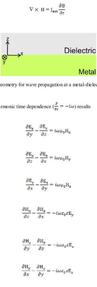
2.4 Surface Plasmons at Metal-Dielectric Interface
Starting with the wave equation, surface plasmon modes can be derived from Maxwell’s equations. If we assume a nonmagnetic media and ignore the dependence of ε over distance, simplified wave equation is given by
(2.12)
Due to a harmonic time dependence, it can be written that E(t) = Ee-iωt and inserting this into the wave equation results
(2.13)
If we consider such a propagation geometry as shown in Figure 2.3, ε is said to be depending only on z-direction since the wave propagates in x-direction without having spatial variations in y-direction. The new wave equation for surface plasmons can be written as E(z)e-iβx where β is the propagation constant along the x-direction. Then the wave equation becomes
(2.14)
where is the wave number of the propagating wave in vacuum.Equation 2.14 is also valid for H field component. More simplified expressions for E and H fields are needed which can be achieved by using the following curl equations
13
(2.16)
Figure 2.3: Geometry for wave propagation at a metal-dielectric interface.
Considerin harmonic time dependence ( ) results
(2.17) (2.18) (2.19) (2.20) (2.21) (2.22)
14 Since the propagation takes place in the x-axis ( ) and homogeneity exists in the y-axis ( ), the previously given set of six equations can be rewritten as (2.23) (2.24) (2.25) (2.26) (2.27) (2.28)
These equations can be categorized for transverse magnetic (p polarized) and transverse electric (s polarized) modes. Ex, Ez and Hy componnets are nonzero for TM mode whereas Hx, Hz and Ey are nonzero for TE mode. Then field components and the wave equation for TM mode become
(2.29)
15
(2.31) For TE mode similar equations appear as
(2.32)
(2.33)
(2.34)
Now we can write propagating surface plasmon wave solutions confined to a metal-dielectric interface. As indicated before, propagation direction is in the x-axis and an evanescent decay occurs in z-x-axis. Adjusting TE mode equations for z > 0 yields
(2.35)
(2.36)
(2.37)
Adjusting TE mode equations for z < 0 yields
(2.38)
16 (2.40)
At the interface where z = 0, continuity of Ey and Hx requires that
(2.41)
(2.42)
Since km and kd are positive, Am have to be zero which requires Am = Ad = 0 in
order to make Equation 2.42 valid. Therefore, surface plasmons can not be excited in TE mode. Now, we will proof that surface plasmon modes can exist in TM polarization. Adjusting TM mode equations for z > 0 yields
(2.43)
(2.44)
(2.45)
Adjusting TM mode equations for z < 0 yields
(2.46)
(2.47)
17 At the interface where z = 0, continuity of Hy and Ex necessitates that
(2.49)
(2.50)
It is important to notice that kd and km are positive, so dielectric permittivities
of the media have to be of the opposite signs to verify Equation 2.50. Since the permittivity of dielectric materials is usually positive, then the real part of the permittivity of the metal has to be negative. Metals such as silver, aluminum and gold provide this condition in the visible and near- infrared wavelengths. These metals also have nonzero imaginary part for permittivity which results in a nonzero imaginary part for the propagation constant of surface plasmon. The reason for the attenuation of the surface plasmon wave in the direction of propagation arises from this imaginary part of β. As a result, it is clear that surface plasmons can be excited only at the interface of the materials with dielectric constants of opposite signs such as a metal-dielectric interface. Further, Hy should also satisfy Equation 2.31, yielding
(2.51)
(2.52)
The dispersion relation of surface plasmons is found by inserting Equation 2.50 into Equations 2.51 and 2.52 which is given as
(2.53)
As a result, we have proved that surface plasmon modes can only be excited in TM polarization.
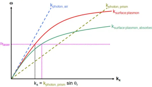
18 Figure 2.4: Dispersion curves and photonic lines for air and silica.
Thanks to the difference between k0 and β, direct excitation of surface
plasmons in a metal-dielectric interface is not possible. Figure 2.4 shows that, there is no intersection points for dispersion curves except origin. In order for surface plasmons to be excited by light, energy and momentum match condition have to be satisfied. Several coupling techniques have been proposed for this purpose which will be discussed in the following subsection.
2.5 Excitation of Surface Plasmons
In surface plasmon resonance sensors, a light wave is used to excite surface plasmon waves and this interaction on the characteristics of the light wave is measured. These measurements provide the changes in propagation constant of a surface plasmon wave. Excitation of a surface plasmon wave by light can occur only if the component of the incoming light’s wave vector that is parallel to the metal surface matches that of the surface plasmon wave. In other words, when the momentum of an incident photon matches that of a surface plasmon, the energy of
19 the beam is absorbed to excite surface plasmons where the intensity of the reflected light is dramatically declines. This resonance condition is sensitive to variations of the medium surrounding a metal surface, so that by measuring the resonance shift in incident angles or wa velenghts, even small refractive index changes on a metal surface can be analyzed.
Surface plasmons can not be directly excited on a flat metal surface since dispersion curve for surface plasmon lies below the light line of the dielectric. In order to overcome this problem, the in-plane momentum of the incident light must be suitable increased. This can be achieved by using special phase matching techniques. The most common techniques are charged particles, prism coupling, grating coupling, waveguide coupling, highly focused optical beams and near field coupling. Here, we will discuss prism and grating coupling methods. More information can be found elsewhere [14-16].
2.5.1
Prism Coupling
The most common approach to excitation of surface plasmons is attenuated total reflection (ATR) based prism coupling. As mentioned before, propagation constant of surface plasmon goes beyond the wave vector of the light in air unless
ω approaches to zero.
(2.54)
Since , addition of a high index prism increases which decreases the slope of the dispersion relation line for light wave giving an intersection point with the surface plasmon dispersion curve (Figure 2.5). This intersection enables the excitation of surface plasmon since energy and momentum match of photon and plasmon is provided. Different resonance angle
20 is obtained if the dielectric medium is changed. This change can even be provided by an adsorption of a material which alters the refractive index and the propagation constant of the surface plasmon.
Figure 2.5: Dispersion relation for prism coupling.
There are two configurations for excitation of surface plasmons with prism coupling method. These are Otto [17] and Kretschmann [18] geometries. In Figure 2.6, Otto configuration is seen where the dielectric layer is between the prism and the metal. Here, the total internal reflection (TIR) takes place at the prism-dielectric interface. The evanescent field at the prism surface tunnels across the dielectric layer and excites surface plasmons on the metal-dielectric interface under the TIR condition. In order to obtain high coupling efficiencies, the thickness of the dielectric layer has to be adjusted properly with the dielectric constant of the dielectric layer since the tunnelling is very susceptible to the characteristics of the dielectric layer.
Although the Otto configuration is preferred in some conditions such as the direct contact with the metal is not wanted, it is quite uncommon due to the very sensitive property of dielectric layer thickness which can even be distorted by small particles like dust particles.
21 Figure 2.6: Otto configuration for prism coupling.
Another prism coupling technique is Kretschmann geometry which is rather widespread due to its simplicity, sensitiveness and easy implementation. In Figure 2.7, this configuration is illustrated where the metal layer is between the prism and the dielectric layer. Here, light passes through a high index prism and its wave vector increases from k0 to nprismk0 .
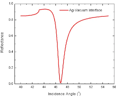
22 The total internal reflection occurs at the prism- metal interface generating an evanescent wave at the prism surface which penetrates across the metal layer while oscillating the free electrons of the metal. When the resonant condition is provided, the energy of the photon is transferred to surface plasmons and excitation takes place on the metal-dielectric interface . Shortly, the vice versa situation of Otto configuration happens.
Due to the energy and momentum transfer in the resonance condition, reflection measurements indicate a characteristic dip (Figure 2.8). This coupling condition is given by
(2.55)
where the momentum component of the incoming light that is parallel to the surface should match with the momentum of the surface plasmon on metal-dielectric interface.
23 In order to observe the sharpest resonance, the metal layer has an optimum thickness value. If the metal layer is too thin, most of the intensity will travel through the metal and propagate freely as a reflected or transmitted wave since the interaction with the electrons can not wholly develop. If the metal layer is too thick, the intensity will not reach to the metal-dielectric interface rather it will reflect where metal is considered to be acting like a mirror.
Many applications have benefited from prism coupling technique so far. It is shown to be very useful for especially characterization of large thin film structures [19]. However several drawbacks such as high cost and large area requirement exist. A more convenient way for surface plasmon excitation is grating coupling.
2.5.2
Grating Coupling
A grating is basically defined as a regular repetition of a periodic pattern (Figure 2.9). Periodic corrugation of a metal-dielectric interface causes the incoming wave to be diffracted by forming series of beams directed away from the surface at a variety of angles. The parallel component of the momentum of the diffracted beams along the interface is different from that of the incoming light by multiples of the grating wave vector. The wave vecto r of the incident photons give rise to diffracted orders. Excitation of surface plasmons occur when the total momentum component of a diffracted order along the interface is equal to that of the surface plasmon wave.
The grating period has to be comparab le with the wavelenght of the incoming light. For a grating period Λ, the coupling condition is given by
24 where is the angle of incidence and m is an integer refering to the diffraction order. By scanning the incident angle or the wavelength of the light , excitation of surface plasmons can be observed. More elaborate demonstration of the coupling condition can be formulated as
(2.57)
(2.58)
Figure 2.9: Grating coupling configuration.
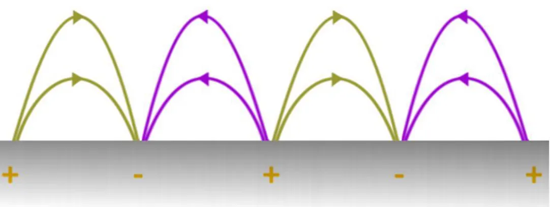
Unlike prism coupling, in grating coupling, the propagation direction of the surface plasmons can be either in the same or in the opposite direction of the surface parallel component of the incoming light wave. The reason for this comes from forward and backward propagation of the diffracted beams along the surface which also adds ± sign to the formula given in Equation 2.58. If surface plasmons travelling in both directions can be provided, multiple dips are observed in reflectivity measurements (Figure 2.10).
25 Figure 2.10: Multiple dips in reflectivity for grating coupling configuration.
26 Figure 2.11 illustrates the effect of corrugation of the surface on the dispersion relation. The periodicity of the grating structure is expresses as one dimensional lattice with spacing , the grating wave vector. The lattice points are scattering centres that can add or subtract momentum from the incident photon in integer multiples of except for 0th order. The zeroth order can not be used for coupling of surface plasmons because of the disparity in Equation 2.54. Excitation can be observed at the crossing points of in-plane photonic dispersion lines and plasmonic dispersion curves.
An important advantage of grating coupling technique comes from its easy fabrication techniques. Grating structures can be manufactured by using several techniques such as interference lithography, electron-beam lithography, photolithography and nanoimprint lithography which makes this method suitable for mass production. However, a disadvantage of grating coupled plasmonic sensing is that in grating-based systems, unlike prism-based systems, the light is introduced through the dielectric layer which requires the whole dielectric medium, including the analytes and microfluidic channels, to be optically transparent.
27
CHAPTER 3
SIMULATIONS
Up to this point, historical progress and theoretical background of surface plasmons have been mentioned. Particularly, very related about the surface plasmon theory, electromagnetic wave behaviour at a metal-dielectric interface and the dielectric function of a metal have been discussed. Since all of the surface plasmon resonance sensors use a coupling technique, excitation geometries have been considered as a keypoint and received an elaborate explanation. One of the coupling tecniques, grating coupling, paves the way for the remaining part of this thesis that’s why it should be understood clearly. Refer to Section 2.2.5.2 for details. Now, we will concentrate on simulations regarding the designed and fabricated sensor structure.
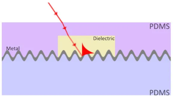
All the simulations presented here were made by using PCGrate Version 6.2 software. Simulations were carried out for a special microstructure design which is illustrated in Figure 3.1. Here, 2-D view is given. Four different layers exist where two of them are composed of an elastomeric material PDMS, poly(dimethylsiloxane). The remaining two are metal and dielectric layers. The metal coating layer has a thickness of 50 nm. Incoming electromagnetic wave is shown with red arrows which respectively pass the PDMS and dielectric layers. PDMS has a refractive index of ̴ 1.45 which was previously reported by Wu et al [20]. In our simulations it is taken as 1.45. The dielectric layer corresponds to the
28 inside of microfluidic channel which will be medium for different liquids; distilled water, solution of 0.9% NaCl and isopropyl alcohol (IPA). In addition to these three liquids, no liquid case ,meaning air only situation, is also considered in simulations. According to [21], the refractive indices are taken as
nair = 1.0003
nwater = 1.3330
n0.9%NaCl = 1.3346
nIPA = 1.3772
Figure 3.1: Simulated Structure.
Two types of modes which are wavelength and angular interrogation, were utilized in simulations. In wavelength interrogation, spectral scanning of wavelengths is employed at a constant incidence angle whereas in angular interrogation, angles are scanned at a fixed wavelength.
29
3.1 Angular Interrogation Simulations
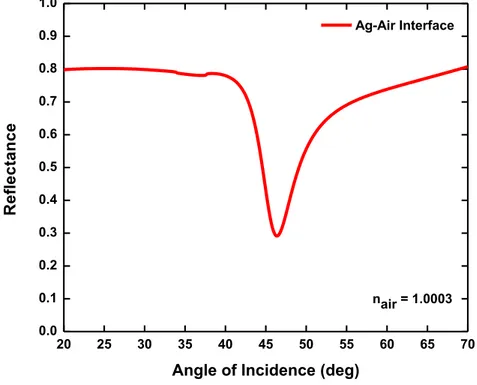
Angle of incidence scan is performed at an incoming light wavelength of 450 nm. The range of the angular interrogation is chosen between the degrees 20˚ and 70˚. The reason for this limitation is that no significant change occurs below 20 and above 70 degrees for incidence angle. The scanning angle resolution is selected as 0.1 degrees which is well beyond the required. The grating structure is a perfect sinusoidal and has a period of 740 nm which is also the period of a DVD grating. Finally, silver is used as the metal layer having a thickness of 50 nm. Four different liquids are used as dielectric layer. Figures 3.2-3.6 show the simulation results for reflected intensities when TM mode is applied.
Figure 3.2: Reflection spectrum with respect to incident angle when air is used as the dielectric layer.
20 25 30 35 40 45 50 55 60 65 70 0.0 0.1 0.2 0.3 0.4 0.5 0.6 0.7 0.8 0.9 1.0 nair = 1.0003 R e fl e c ta n c e
Angle of Incidence (deg)
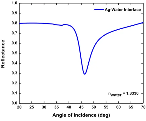
30 Figure 3.3: Reflection spectrum with respect to incident angle when water is used as the dielectric layer.
Figure 3.4: Reflection spectrum with respect to incident angle when 0.9% NaCl solution is used as the dielectric layer.
20 25 30 35 40 45 50 55 60 65 70 0.0 0.1 0.2 0.3 0.4 0.5 0.6 0.7 0.8 0.9 1.0 R e fl e c ta n c e
Angle of Incidence (deg)
Ag-Water Interface nwater = 1.3330 20 25 30 35 40 45 50 55 60 65 70 0.0 0.1 0.2 0.3 0.4 0.5 0.6 0.7 0.8 0.9 1.0 nIPA = 1.3772 R e fl e c ta n c e
Angle of Incidence (deg)
31 Figure 3.5: Reflection spectrum with respect to incident angle when isopropanol is used as the dielectric layer.
Figure 3.6: Reflection spectra with respect to incident angle for all the simulated materials. 20 25 30 35 40 45 50 55 60 65 70 0.0 0.1 0.2 0.3 0.4 0.5 0.6 0.7 0.8 0.9 1.0 R ef le ct an ce
Angle of Incidence (deg)
Air Water 0.9% NaCl IPA 20 25 30 35 40 45 50 55 60 65 70 0.0 0.1 0.2 0.3 0.4 0.5 0.6 0.7 0.8 0.9 1.0 n0.9%NaCl solution = 1.3346 R e fl e c ta n c e
Angle of Incidence (deg)
Ag-0.9% NaCl interface
45.0 45.2 45.4 0.280
0.282 0.284
32 Simulation results reveal that the angle of incidence where the plasmonic excitation occurs depend on the dielectric material type. The effecting parameter is the refractive index of the dielectric if scattering and absortion losses are neglected. We have theoretically proved this dependence with the simulations. When air is used as the dielectric layer, the resonance angle is found as 29.1 whereas this number shifted to 45.1 in water, 45.2 in 0.9% NaCl solution and 46.4 in IPA cases. As given before, air has the lowest and IPA has the highest refractive index of these materials. Related to this, resonance angle for air was detected as the smallest of all four materials whereas that of it for IPA was the biggest.
In order to determine the sharpness of the resonance curves, the angular quality factors (AQF) are calculated which is defined as the ratio of the resonance angle to FWHM. The AQF values for the aforementioned materials are found to be varying between 17 and 19.
3.2 Wavelength Interrogation Simulations
In some cases, interrogation type effects the sensitivity and sharpness of the resonances that’s why wavelength scan is also performed. The interval for wavelength scan is selected as 400-1100 nm since coupling of surface plasmons does not take place outside this range for the constant angle of incidence at 20˚. Although 1 nm resolution for the wavelength scan gives sufficient results, it is selected as 0.2 nanometers in order to collect more data points and fit more accurate graphs. The same grating structure, metal and dielectric layer parameters are used as the angular interrogation case. Figures 3.7-3.11 show the simulation results for reflected intensities for an incoming light with TM mode.
Reflectance simulations with respect to wavelength indicate that the wavelength where the coupling of surface plasmons to the dielectric- metal
33 interface occurs, depends on the dielectric material selection. Resonant wavelengths shift even for tiny changes in refractive indices of the dielectric medium. As previously done in angular interrogation case, this time we have theoretically showed this dependence by using wavelength interrogation simulations.
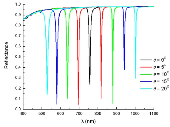
When air is used as the dielectric layer, the resonance wavelengths are placed at 530 nm and 1002.6 nm. The reason for double resonances comes from a number of diffracted orders which can couple to surface plasmons propagating forward and backward directions. The coefficient m in Equation 2.56 stands for the orders. In some cases, for different values of m, the equation can be satisfied, resulting in multi dips in reflectance spectra. Also in Figure 2.11, it is shown that more than one dispersion curve can intersect the photonic dispersion lines.
If water is used as the dielectric layer, the major resonance wavelengt sits at 697.6 nm while a minor resonance also exists at 788.2 nm. In 0.9% NaCl case, the major and minor resonances are respectively at 698.4 nm a nd 788.4 nm whereas they are respectively 719.2 nm and 782.2 nm for IPA situation.
As provided before, air has the lowest and IPA has the highest refractive index of these materials. Related to this, resonance wavelength for air was detected as the smallest of all four materials whereas that of it for IPA was the biggest. Although, index of refraction gives information about the wavelenghts that excitation occurs, it is not the only determining parameter. The period of the grating also plays role in resonance conditions. This fact can also be understood from the Equations 2.56-2.58. In our case, when the period is increased, the resonances shift to larger wavelengths.
The resonances obtained from wavelength interrogation scans have better sharpness values than that of it acquired from angle based scans. The quality factors for wavelength scan utilizing the major resonance mode are calculated and
34 found to be varying between 45 and 230. Wavelength quality factors are found as 230 for air, 48 for water and 0.9% NaCl, 60 for IPA cases. It is clearly seen that the Q-factors for wavelength scan case is much larger than the angular scan case which was between 17 and 19. This can also be understood from the water and 0.9% NaCl cases. In angular scan mode, the resonance angle shift was found to be 0.1 degress whereas in wavelength scan mode, it is 0.8 nm. In other words, detectibility of the change in resonance parameters is more accurate and obvious for wavelength interrogation mode.
As a result, considering the simulation parameters, wavelength scan is more preferable in terms of sensitivity since a sharper resonance improves the overall sensitivity of plasmonic device. Furthermore, high Q-factors yield higher field enhancement factors which is important in some application such as surface enhanced Raman scattering.
Figure 3.7: Reflection spectrum with respect to wavelength when air is used as the dielectric layer. 400 500 600 700 800 900 1000 1100 0.0 0.1 0.2 0.3 0.4 0.5 0.6 0.7 0.8 0.9 1.0 nair = 1.0003 R e fl e c ta n c e Wavelength (nm) Ag-Air Interface
35 Figure 3.8: Reflection spectrum with respect to wavelength when water is used as the dielectric layer.
Figure 3.9: Reflection spectrum with respect to wavelength when 0.9% NaCl solution is used as the dielectric layer.
400 500 600 700 800 900 1000 1100 0.0 0.1 0.2 0.3 0.4 0.5 0.6 0.7 0.8 0.9 1.0 nwater = 1.3330 R e fl e c ta n c e Wavelength (nm) Ag-Water Interface 400 500 600 700 800 900 1000 1100 0.0 0.1 0.2 0.3 0.4 0.5 0.6 0.7 0.8 0.9 1.0 n0.9%NaCl = 1.3346 Ag-0.9% NaCl Interface
R e fl e c ta n c e Wavelength (nm)
36 Figure 3.10: Reflection spectrum with respect to wavelength when isopropanol is used as the dielectric layer.
Figure 3.11: Reflection spectrum with respect to wavelength for all the simulated materials. 400 500 600 700 800 900 1000 1100 0.0 0.1 0.2 0.3 0.4 0.5 0.6 0.7 0.8 0.9 1.0 R e fl e c ta n c e Wavelength (nm) Air Water 0.9% NaCl IPA 400 500 600 700 800 900 1000 1100 0.0 0.1 0.2 0.3 0.4 0.5 0.6 0.7 0.8 0.9 1.0 nIPA = 1.3772 Ag-IPA Interface R e fl e c ta n c e Wavelength (nm) 696 698 700 0.06 0.09 0.12
37 Figure 3.11 illustrates the resonances for different dielectric materials. Here, as stated before, the effect of refractive index of the dielectric to the resonance wavelengths is quite evident. Even a change of 0.0016 in index of refraction yields a shift of 0.8 nm in wavelength which is zoomed and demonstrated as inset.
38
CHAPTER 4
FABRICATION and
CHARACTERIZATION
The experimental techniques will be discussed in this chapter. Utilization of optical discs for grating fabrication, soft lithography, optical lithography and plasma oxidization methods will be examined thoroughly. Characterization studies of grating depth and metal layer thickness will also be investigated. Atomic force microscopy images will be provided for better understanding of the surface topographies.
4.1 Fabrication and Characterization of Gratings
In order to fabricate gratings, several techniques such as interference lithography, electron-beam lithography, photolithography, nanoimprint lithography and soft lithography are available. Soft lithographic techniques are utilized in our studies.
4.1.1
DVDs as a Grating Source
Commercially available digital versatile discs (DVDs) are mass produced by injection molding techniques and serve as inexpensive grating subtrates. Recently
39 reported studies show the exploitation of DVDs as grating sources [22,23]. For applications regarding grating coupled plasmonics, surfaces of the DVDs have to be subjected to modifications in terms of grating depth since in order to observe sharp resonances, grating depths must lie within a restricted range By using several chemical procedures, the surface profile can be tuned for high Q-factors.
Selection of the DVD type is worth to mention since not all DVDs have the same fabrication technology. DVD-R type discs are used since they have a dye layer as the recording medium that can be dissolved easily in acetone or isopropanol. DVD-RW type discs generally utilize a hard chalcogenide materials the recording medium which is not suitable for further manipulations.
Figure 4.1: DVD handling processes. (a) Cutting a notch into the side of the DVD. (b,c) Peeling apart the disc layers of the DVD. (d) Seperated disc layers of the DVD.
40 The handling procedure for DVDs is shown above. First, by using a scissors, a notch cut is made mechanically into a side of the disc. This cut provides a location for separation. Then, the discs are removed by applying mechanical force. Finally, disc pairs are completely separated. After notch cutting process, 1 minute oven bake at 70 ˚C is found to be facilitating the layer separation process. As seen in Figure 4.1d, two disc layers have different views. The one on the left side has a metal coating layer different from the right one. Although both of these discs can be used for grating fabrication, we prefer to choose the one of the left side which has a thin metal layer. If the disc on the right side is used, the violet dye layer is removed by washing with isopropanol first. Then, the cleaned layer is immersed into 4:1 mixture of isopropanol and acetone solution in order to etch the grating.
It was reported that grating depths of 20 to 60 nm result in sharp resonances with full width at half maxima less than 10 nm [22]. In order to achieve these values, etching process time should be controlled. Unetched DVD-R profiles vary between 100 and 120 nm depending on the manufacturer. These values are not optimal for observing sharp and strong resonances. Also the gra ting pattern of an unetched disc is not a perfect sinusoidal pattern. After etching, surface profile becomes nearly a perfect sinusoidal as seen in Figure 4.2. Here, etching times of 30-60 seconds yielded a surface profile well enough for sharp resonances. Slight agitation during etching was observed to be effecting the uniformity of the grating depths.
Figure 4.2: Profiles of the gratings on a DVD-R disc for various etching times.
0.0 0.2 0.4 0.6 0.8 1.0 1.2 1.4 0 20 40 60 80 100 120 140 unetched
30 sec etching 60 sec etching
D e p th ( n m ) Distance (m)
41 Although it seems to be giving good results, we will not use the disc on the right side of the Figure 4.1d due to several reasons. These discs are made of polycarbonate disc pairs. Acetone alone damages the polycarbonate layer which is not coated with a metal. When diluted with isopropanol, the damaging disappears, instead etch process dominates but still in some cases this method is not very reliable since acetone- isopropanol mixture is assumed to be perfectly homogeneous and it is assumed that in every point of the solution, the 4:1 ratio is maintained. However, as seen in Figure 4.3b, even adjacent gratings in the same line has noteworthy variations in terms of grating depth. The depth of the grating shown with the red cursor is nearly 52 nm whereas that of it for green cursor is approximately 60 nm. It is meant that acetone- isopropanol (4:1) mixture does not etch the discs properly. Applications that require exact values of gratings may suffer from this technique and also a mismatch may appear between theoretical simulations and experimental results. Atomic force microscopy (AFM) images were taken by PSIA XE 100.
Figure 4.3: (a) AFM topography image of the etched polycarbonate disc. (b) Line profile showing the depth of the gratings.
42 Instead of employing the aforementioned etching method and using the metal free polycarbonate disc, the metal coated disc layer which is shown on the left side of Figure 4.1d is utilized. We get rid of etching process by spin coating a thin film resist in order to fill the grating trenches resulting in a lower depth grating. Since the polycarbonate disc is coated with a metal, generally aluminum, treatment with acetone does not damage the disc on the contrary it removes the dye layer rapidly and neatly. Figure 4.4 shows the procedure for obtaining desirable grating depths. Acetone is used to remove the dye layer. Washing with isopropanol provided the surface cleaning. Dry nitrogen flow removed the remaining liquid droplets. A slice is cut from the disc in accordance with the dimensions of the final situation of the fabricated structure. In order to decrease the depth of gratings, a thin film resist, poly(methyl methacrylate) (PMMA) is spin coated onto the sliced disc piece. PMMA sticks well to almost any surface and lasts forever.
Figure 4.4: (a) Acetone treatment. (b) Isopropanol treatment. (c) Drying with dry nitrogen flow. (d) Dried disc. (e) Slice from the disc. (f) PMMA spin coating.
43 Spin coating is basically a process to produce thin films. A small puddle of a liquid resist is poured onto the substrate and applying a high rotational speed, resist spreads to the substrate and gets thinner. We spinned PMMA resist (950 PMMA A2, in Anisol, MicroChem Corp.) onto the previously sliced disc piece.
Figure 4.5: Thickness variation with spin speed for 950K PMMA A2, in Anisol.
A spin rate of 5000 rpm is applied for 60 seconds following a 5 second 500 rpm step which corresponds to 25 nm thickness (Figure 4.5). Although 90 seconds oven bake at 180 ˚C is performed in general, we prefer to make it 10 minutes at 90 ˚C in order to evaporate the solvent and keep the disc intact. The reason for this different procedure arises from the fact that the structural distortion of the DVD takes place at temperatures more than 100 ˚C. Prior to resist spinning, metal coated polycarbonate side had a grating depth of 80-82 nm which is shown is Figure 4.6. PMMA thickness of 25 nm fills the trenches of the gratings and forms a 55 nm deep gratings. It should be noted, contrary to etching case where more than 10 nm deviations are observed, this method yields grating depth variat ions of only ± 2 nm. Moreover, the sinusoidality of the gratings in this case is nearly perfect and better than that of it for etched situation. Also resist spinning offers repeatable results unlike etching technique. PMMA spinned surface topography and line profiles are provided in Figure 4.7.
44 Figure 4.6: (a) AFM topography image of the metal coated polycarbonate disc side. (b) Line profile showing the depth of the gratings.
45 Figure 4.7: (a) AFM topography image following PMMA spin. (b) Line profile showing the depth of the gratings.
4.1.2
Soft Lithography
Soft lithography is essentially a process that allows a pattern on a master to be embossed onto a soft substrate. Soft lithographic techniques are convenient, effective, low in capital cost, easy to perform and quick to make many structures from the same master. It is a non-photolithographic technique that’s why diffraction limitations is eliminated. Features on the nanometer scale can even be obtained. It is named “soft” since elastomeric materia ls are used in this technique.
46 Although several elastomers have been reported such as polyurethanes and polyimides [24], the most popular elastomeric material is poly(dimethylsiloxane) (PDMS). PDMS is a very useful material in soft lithography since it
makes conformal contact with the surfaces over large areas,
provides a surface that has a low interfacial free energy and good stability resulting in a reversible adhesion of patterned molecules,
does not swell in humidity,
allows the passage of gases from its membrane,
provides good thermal stability allowing thermal curing of the molded polymers and
enables UV cross-linking for molded pre-polymers due to its transparency down to 300 nm [24].
PDMS offers unique properties owing to the presence of organic methyl groups attached to silicon and an inorganic siloxane backbone. They are fluids at room temperature due to their very low transition temperatures and are easily solidified by cross- linking. In our case, we used PDMS (Sylgard 184, Dow Corning) which is supplied as a two-part kit: a liquid silicon rubber pre-polymer base and a curing agent. First, 10:1 mixture of base and curing agent is poured onto a clean petri dish and mixed with a clean plastic stir rod until the mixture gets milky color due to air bubbles. Improper mixing may leave behind unreacted curing agent with unfavorable bonding results. Also, it is better to weight the curing agent first then add the pre-polymer base after. Since we want to transfer the gratings to PDMS, the mixture is poured onto the PMMA coated disc slice. Then, disc is put into a vacuum chamber for the removal of air bubbles which lasts approximately 15-20 minutes. In some cases, bubbles can still remain on the surface. In order to remove them, blowing gently or popping with a sharp needle or tweezer can be employed. It should be noted that, degassing of the PDMS may take up to an hour depending upon the pattern profile and size of the mold. Degassed PDMS along with the disc is subjected to thermal treatment to solidify the mixture. Several baking options are reported in the literature such as thermal
47 baking using oven or hot plate at 65 ˚C for 4 hours or at 80 ˚C for 2 hours or 105 ˚C for 1 hours [25,26]. These are the minimum required conditions for the curing of PDMS. Higher temperatures are observed to be yielding better curing results but the disc structure is deformed at very high temperatures above 100 ˚C. We prefer to use oven bake at 75 ˚C for at least 4 hours. Thermal treatment basically provides cross- linking of the elastomer (PDMS) via the hydrosilylation reactions between vinyl (SiCH=CH2) groups and hydrosilane (SiH) groups. PDMS molded disc is shown in Figure 4.8a where the mold is stick to the disc.
Figure 4.8: (a) PDMS molded disc. (b) Peeling off the PDMS mold. (c) PDMS mold having the replica of the pattern on the disc surface.
Using a tweezer, peeling off the mold from the master (disc) is performed carefully (Figure 4.8b). It is important to be very gentle throughout the unmolding process since most master or mold breakages occur during unmolding.
Figure 4.9: PDMS molding steps from a master having gratings on its surface (a) Master surface topography. (b) Pouring of PDMS over master. (c) PDMS mold.
48 Figure 4.10: (a) AFM topography image of the PDMS mold. (b) Line profile showing the depth of the gratings.
The surface topography investigations show that the grating depth of the PDMS mold is approximately 50 nm which is ̴ 5 nm less than that of it for PMMA spinned disk.
49
4.1.3
Metal Deposition
As we discussed in Section 2.2.1, plasmonic excitation requires a thin metal film layer. The choice of this material in contact with aqueous solutions is one significant parameter for an optimized plasmonic coupling. Silver, gold, aluminum and copper are several suitable metals [27,28]. Although gold is widely used due to its highly stable chemical and optical properties, sharpest resonances are provided by silver. In air, FWHM for gold is 10.67˚ whereas it is 0.71˚ for silver [29]. When compared to gold, silver is more sensitive to thickness and refractive index variations. Also, penetration depth for silver is larger than that of it for gold. The main weakness of silver is its chemical instability since it oxidizes in air and aqueous solutions, preventing long time measurements. Covering with a thin and protecting layer can solve this problem though [30]. In our case, we deposited 50 nm silver onto the PDMS mold by using thermal evaporation technique. Prior to this, an adhesive stripe is used to define the deposit area (Figure 4.11) since we do not desire all the mold to be coated. After deposition process, the stripe is removed. The restricted area for silver is due to the structural surface deformation of the silver layer in plasma oxidation step which will be discussed in Section 2.4.1.5.
Figure 4.11: (a) Schematic representation of metal coating process. (b) Silver coated PDMS mold
50 Surface topography for silver coated PDMS mold is shown below. It is measured that grating depths are a few nm less than that of it for uncoated PDMS mold case.
Figure 4.12: (a) Topography of the silver coated PDMS mold. (b) Line profile for the silver coated region.