M.Sc. THESIS
February 2016
INCREASING THE EFFICIENCY OF ORGANIC LIGHT EMITTING DIODE BY USING SELF ASSEMBLED MONOLAYER
Thesis Advisor: Assoc. Prof. Dr. Mustafa CAN
IZMIR KATIP CELEBI UNIVERSITY GRADUATE SCHOOL OF SCIENCE AND ENGINEERING
Eyyup YALÇIN
Department of Materials Science and Engineering
Anabilim Dalı : Herhangi Mühendislik, Bilim Programı : Herhangi Program
IZMIR KATIP CELEBI UNIVERSITY GRADUATE SCHOOL OF SCIENCE AND ENGINEERING
February 2016
INCREASING THE EFFICIENCY OF ORGANIC LIGHT EMITTING DIODE BY USING SELF ASSEMBLED MONOLAYER
M.Sc. THESIS Eyyup YALÇIN
(Y130111024)
Department of Materials Science and Engineering
Anabilim Dalı : Herhangi Mühendislik, Bilim Programı : Herhangi Program
ŞUBAT 2016
İZMİR KÂTİP ÇELEBİ ÜNİVERSİTESİ FEN BİLİMLERİ ENSTİTÜSÜ
KENDİLİĞİNDEN ORGANİZE TEK KATMAN TABAKALARI KULLANILARAK ORGANİK IŞIK YAYAN DİYOTLARIN VERİMİNİN
ARTIRILMASI
YÜKSEK LİSANS TEZİ Eyyup YALÇIN
(Y130111024)
Malzeme Bilimi ve Mühendisliği Ana Bilim Dalı
Anabilim Dalı : Herhangi Mühendislik, Bilim Programı : Herhangi Program
Assist. Prof. Dr. Hadi M. ZAREIE ... Izmir Institute of Technology
Thesis Advisor : Assoc. Prof. Dr. Mustafa CAN ... Izmir Katip Çelebi University
Jury Members : Assoc. Prof. Dr. Şerafettin DEMİÇ ... Izmir Katip Çelebi University
Eyyup YALÇIN, a M.Sc. student of IKCU Graduate School of Science and Engineering, successfully defended the thesis entitled’’INCREASING THE EFFICIENCY OF ORGANIC LIGHT EMITTING DIODE BY USING SELF ASSEMBLED MONOLAYER”, which he prepared after fulfilling the requirements specified in the associated legislations, before the jury whose signatures are below.
ACKNOWLEDGMENTS
Many people deserve a thank you for their support during my M.Sc. program and I have already apologized to whomever I am forgetting in the following list. Firstly and foremost, I would like to thank my advisor, Assoc. Prof. Dr. Mustafa CAN, for his leading and support during my master thesis. Then I have to thank Assoc. Prof. Dr. Şerafettin Demiç for his open-minded ideas in this study. Moreover, my fellow lab mates M. Zeliha Yiğit and Emre Arkan deserve my special thanks for supporting me in chemical issue by providing new synthesized materials.
I would like to thank Assoc. Prof. Dr. Mahmut KUŞ who gave me a chance to access the laboratory and research facilities in Selçuk University Advanced Technology Research and Application Centre. I also wish to express my gratitude for Koray Kara and Duygu Akın Kara. It would have been impossible to achieve these research results without their help and experience. In addition, I want to thank my dear friend Veysel Ulaş for his help to organize this thesis.
Last but not least, I would like to thank my family. I cannot find words to express my thanks for their helps.
TABLE OF CONTENTS
Page
ACKNOWLEDGMENTS ... vii
TABLE OF CONTENTS ... viii
ABBREVIATIONS ... ix LIST OF TABLES ...x LIST OF FIGURES ... xi ABSTRACT ... xii ÖZET... xiii 1. INTRODUCTION ...1
1.1 Organic Light Emitting Diodes ... 1
1.2 Device Structure of OLEDs ... 4
1.3 Charge Injection ... 5
1.4 Materials ... 7
1.4.1 Anode materials ...7
1.4.2 Hole transport materials (HTL) ...7
1.4.3 Electron transport and emissive materials (ETL and EM) ...8
1.4.4 Cathode materials ...9
1.5 Self-Assembled Monolayers ... 9
1.6 OLED Efficiency ...11
2. EXPERIMENTAL DETAILS ... 13
2.1 The Steps of OLED Preparation...13
2.2 Etching, Cleaning and Oxygen Plasma procedure for ITO ...13
2.3 Surface Treatment of ITO by Using SAM Technique ...14
2.4 Thermal Evaporation of Organic Layers and Metallic Layer ...15
2.5 Characterization of OLED Devices ...17
2.5.1 AFM surface characterization ... 18
2.5.2 Kelvin probe force microscopy (KPFM) surface characterization ... 19
2.5.3 Cyclic voltammetry characterization ... 20
2.5.4 Contact angle characterization ... 20
3. RESULT AND DISCUSSION ... 22
3.1 Electrical and Optical Characterization Results ...22
3.1.1 Cycle voltammetry results ... 22
3.1.2 Electrical and optical characterization of 4,4''-di-9H-carbazol-9-yl-1,1':3',1''-terphenyl-5'-carboxylic acid (CAR) ... 24
3.1.3 Electrical and optical characterization of 4,4''-bis(diphenylamino)-1,1':3',1''-terphenyl-5'-carboxylic acid (TPA) ... 29
3.1.4 Electrical and optical characterization of ‘TPA and CAR’ materials ... 33
3.2 Surface Characterization Results ...38
3.2.1 Atomic force microscope results ... 38
3.2.2 Kelvin probe force microscope results ... 39
3.2.3 Contact angle results ... 42
4. CONCLUSIONS ... 43
ABBREVIATIONS AND SYMBOLS
a.u : Absorption unit
AFM : Atomic Force Microscope Ag : Silver Al : Aluminum Au : Gold Ca : Calcium cd : candela EL : Electrolunminesence EML : Emissive Layer
EQE : External Quantum Efficiency ETL : Electron Ttransport Layer ev : Electron Volt
HOMO : Highest Occupied Molecular Orbital HTL : Hole Transport Layer
HTM : Hole Transport Material IQE : Internal Quantum Efficiency ITO : Indium Thin Oxide
J : Current Density
KPFM : Kelvin Probe Force Microscope L : Luminance
LCD : Liquite Crystal Diode Li : Lithium
lm : lumen
LUMO : Lowest Unoccupied Molecular Orbital
M : Molar
Mg : Magnesium
MoO3 : Molybdenum trioxide
N : Nitrogen
ŋce : Current Efficiency
ŋext : External Quantum Efficiency
ŋint : Internal Quantum Efficiency
ŋp : Power Efficiency
OLED : Organic Light Emitting Diode RMS : Root mean square
SAM : self Assemble Monolayer Tg : Glass Transition Temperature
VCPD : Contact potential difference
W : watt
γlv : liquid-vapor surface tension
γsl : solid- liquid surface tension
γsv : solid-vapor surface tension
LIST OF TABLES
Page
Table 2.1 : Configuration of OLED devices ...17
Table 3.1 : Device numbers and their structures ...25
Table 3.2 : Electrical and Optical details about devices ...29
Table 3.3 : Device structures and theirs numbers ...30
Table 3.4 : Electrical and Optical details about devices. ...33
Table 3.5 : Device numbers and structures ...34
Table 3.6 : Electrical and Optical details about devices ...37
Table 3.7 : Surface roughness of Bare ITO, ITO/CAR, ITO/TPA and ITO/TPD/Alq3 ...38
LIST OF FIGURES
Page
Figure 1.1 : LG OLED display (a) and OLED for lighting applications (b) [6] ... 3
Figure 1.2 : OLED materials can be deposited on flexible substrate ... 3
Figure 1.3 : General Structure of an OLED ... 4
Figure 1.4 : Hole and electron injection from electrodes to organic layers. ... 6
Figure 1.5 : OLED structure with the hole and electron blocking layers. ... 6
Figure 1.6 : Chemical Structure of TPD (a) and NPB (b)... 7
Figure 1.7 : Chemical Structures of Alq3 (a), Gaq3 (b) and Inq3 (c)... 8
Figure 1.8 : Schematic illustration of SAMs (a) – Generation of SAMs on a substrate (b) 10 Figure 1.9 : Surface coverage of SAM versus time ...11
Figure 2.1 : Manufacturing process of OLEDs ...13
Figure 2.2 : Oxygen Plasma Device ...14
Figure 2.3 : Chemical structure of TPA (a) and CAR (b) Molecules ...15
Figure 2.4 : Organic (a) and Metallic (b) Evaporation Systems ...16
Figure 2.5 : General work principle of AFM ...18
Figure 2.6 : Nanosurf Flex AFM (right) and its software (left) ...19
Figure 2.7 : Typical current vs potential graph of CV ...20
Figure 2.8 : Illustration of contact angles on a smooth solid surface . ...21
Figure 3.1 : CV Voltammogram of modified ITO with TPA ...23
Figure 3.2 : CV Voltammogram of modified ITO with CAR ...23
Figure 3.3 : Energy diagram of OLED devices with TPA (a) and CAR (b) ...24
Figure 3.4 : J-V Characteristic of Device 1 to 4 ...25
Figure 3.5 : Luminance versus Voltage graph of Device 1 to 4 ...26
Figure 3.6 : Current Efficiency vs Luminance graph of Device 1 to 4...27
Figure 3.7 : Power Efficiency vs Luminance graph of Device 1 to 4 ...28
Figure 3.8 : Intensity vs Wavelength graph for Device 1 to 4 ...29
Figure 3.9 : Current Density versus Voltage graph ...30
Figure 3.10 : Luminance versus Voltage graph...31
Figure 3.11 : Current Efficiency versus Luminance graph ...32
Figure 3.12 : Power Efficiency versus Luminance graph ...32
Figure 3.13 : Intensity versus Wavelength Graph ...33
Figure 3.14 : Current Density versus Voltage graph ...35
Figure 3.15 : Luminance versus Voltage graph...35
Figure 3.16 : Current Efficiency versus Luminance graph ...36
Figure 3.17 : Power Efficiency versus Luminance graph ...36
Figure 3.18 : Intensity versus Wavelength graph ...37
Figure 3.19 : AFM images of Bare ITO (a), modified ITO with CAR (b) and TPA (c). After organic materials coating on ITO (d) ...38
Figure 3.20 : AFM topography (a) and surface potantial (b) of bare ITO with KPFM. ....39
Figure 3.21 : AFM topography (a) and surface potential (b) of ITO/CAR with KPFM technique ...39
Figure 3.22 : AFM topography (a) and surface potential (b) of ITO/TPA with KPFM ...40
Figure 3.23 : Surface Potential of Bare ITO ...41
Figure 3.24 : Surface Potential of ITO/CAR...42
Figure 3.25 : Surface Potential of Bare ITO, ITO/CAR and ITO/TPA ...41
INCREASE EFFICIENCY OF ORGANIC LIGHT EMITTING DIODE BY USING SELF-ASSEMBLED MONOLAYERS
ABSTRACT
This study is focused on modification and characterization of indium tin oxide (ITO) substrates with self-assembled monolayers (SAMs) to increase efficiency of Organic Light Emitting Diodes (OLEDs). As known, ITO has widely been used as an anode material in OLED devices because of its high conductivity and high transparency. However the work function between the energy level of ITO electrode and HOMO energy level of organic materials have a large injection barrier. This barrier leads poor charge injection and low efficiency. To solve this problem ITO substrates are modified using SAM materials, hence the energy level of ITO is increased.
In this thesis, 4,4''-bis(diphenylamino)-1,1':3',1''-terphenyl-5'-carboxylic acid (TPA) and 4,4''-di-9H-carbazol-9-yl-1,1':3',1''-terphenyl-5'-carboxylic acid (CAR) molecules were used as SAM materials. After ITO substrates were modified with SAM materials, changing in an energy level of ITO was determined using Cyclic Voltammetry. In addition, the OLED devices which are fabricated with SAM modified ITO show better turn on voltage, luminance, current efficiency, power efficiency and intensity compared to unmodified ITO.
For the surface characterization, Atomic Force Microscope (AFM) was used to analyze surface topography of the modified and unmodified ITO. Also, Kelvin Probe Force Microscope (KPFM) was used to determine changes in the surface potential of modified and unmodified ITO. Finally, surface characterization was analyzed with contact angle measurement. After ITO was modified with CAR and TPA molecules, contact angle variation between modified and unmodified ITO was clearly observed.
KENDİLİĞİNDEN ORGANİZE TEK KATMAN TABAKALARI KULLANILARAK ORGANİK IŞIK YAYAN DİYOTLARIN VERİMİNİN
ARTIRILMASI ÖZET
Bu çalışma, organik ışık yayan diyotların (OLEDs) verimini artırmak için indiyum kalay oksit (ITO) yüzeyinin kendiliğinden organize tek katman tabakaları (SAM) ile modifiye ve karakterizasyonu üzerine yoğunlaşmıştır. Bilindiği gibi, ITO yüksek iletkenlik ve yüksek saydamlık özelliğinden dolayı OLED cihazlarında yaygın olarak anot malzemesi olarak kullanılmaktadır. Fakat metal elektrotun (ITO) çalışma fonksiyonu ile organik malzemelerin HOMO enerji seviyesi arasında yüksek enjeksiyon farkı bulunmaktadır. Bu fark, düşük yük enjeksiyonuna ve düşük verime neden olmaktadır. Bu problemi çözmek için ITO yüzeyleri SAM malzemeleri ile modifiye edilmiştir. Böylelikle ITO nun enerji seviyesi yükseltilmiştir.
Bu tezde SAM malzemeleri olarak 4,4''-bis(difenilamino)-1,1':3',1''-terfenil-5'-karboksilik asit (TPA) ve 4,4''-di-9H-karbazol-9-il-1,1':3',1''-terfenil-5'-4,4''-bis(difenilamino)-1,1':3',1''-terfenil-5'-karboksilik asit (CAR) molekülleri kullanılmıştır. ITO yüzeyleri SAM malzemeleri ile modifiye edildikten sonra, ITO nun enerji seviyesindeki değişim döngüsel voltametri ile belirlenmiştir. Ayrıca, SAM ile modifiye edilmiş ITO yüzeylerinden üretilen OLED cihazları, modifiye edilmemiş ITO yüzeylerinden elde edilen OLED cihazlarına göre daha iyi çalışma gerilimine, parlaklığa, akım verimine, güç verimine ve ışık yoğunluğuna sahiptirler.
Yüzey karakterizasyonu için, modifiye edilimiş ve modifiye edilmemiş ITO yüzeyinin topografyası Atomik Kuvvet Mikroskobu (AFM) kulanılarak analiz edilmiştir. Ayrıca modifiye edilmiş ve modifiye edilmemiş ITO yüzeyindeki potansiyel değişimi Kelvin Prope Kuvvet Mikroskopu (KPFM) ile analiz edilmiştir. Son olarak yüzey karakterizasyonu temas açısı ile incelenmiştir. ITO ‘CAR ve TPA’ molekülleri ile modifiye edildikten sonra, modifiye edilmiş ve modifiye edilmemiş ITO lar arasındaki temas açısı değişimi açıkça gözlemlenmiştir..
1. INTRODUCTION
1.1 Organic Light Emitting Diodes
Energy is one of the main problems in the history of mankind. Especially after the industrial revolution, energy needs increased dramatically. By discovery of carbon based fuel sources, almost all countries shifted their preferences to use this type of energy source. However, excessive use of fuel energy sources causes tragic problems to mankind such as air pollution, which is one of the biggest treats for a human being, recently. Because of this problem, researchers are actively searching the ways for converting green energy sources like solar energy, wind energy, etc, into electrical energy.
There have been many technological applications applied to our life in the past 60 years, which made a big increment in mechanization of human kind. As known, almost every technical equipment consumes energy to produce effective work. Relatedly, a huge amount of fuel source is being used up giving rise to the air pollution. For this reason, researchers densely study on developing energy saving materials for a long time that will decline air pollution. The materials that are used in organic light emitting diodes (OLEDs) are one of these novel materials and scientists have researched by scientists since the discovery of electroluminescence.
The first electroluminescence (EL) property of organic materials in OLEDs was shown by Helfrich and Schneider in 1965 [1]. Nevertheless, it had extremely high turn on voltage (~100V) for which almost no practical application seemed possible for those times. Fortunately, after 22 years later in 1987 the first efficient low-voltage (10V) organic EL was demonstrated by Tang and VanSlyke [2] in Kodak. It is considered as the beginning of the first OLEDs. They fabricated this device with thermal evaporation technique under high vacuum by using small organic molecules. These molecules include N,N-diphenyl-N,N-bis (3-methylphenyl) 1-1’biphenyl – 4,4 diamine (TPD) and tris (8-hydroxyquinoline) aluminum (𝐴𝑙𝑞3) with a total thickness
increased in huge amounts after this invention, which is regarded a milestone in this field. With this development, OLEDs have attracted much attention and taken a part in the market as displays. Another important development about OLEDs occurred in 1990 at the University of Cambridge. In this development researchers obtain electroluminescence from polymers[3]. They used a conjugated polymer, poly-para-phenylene vinylene (PPV)[4], which become the most used polymers in OLEDs. This discovery opens the gate for flexible electronics.
Today OLEDs are used as displays and lighting appliance (Figure 1.1) due to their advantage of low-power consumption, high contrast, high brightness, low weight, high luminous efficiency and wide viewing angle [5]. Due to that they are widely used their electric energy consumption should be lowered. Hence, low power consumption is the most important property for OLEDs. These above listed properties of OLEDs make it advantageous compared to liquid crystal displays (LCDs) in the market. Because, LCD displays use polarized films since the light requires to be polarized. In addition, color filters should also be used in LCDs, because LCDs cannot emit different colors directly like OLEDs. There is an instant light loss of 50% due to the problem of polarized films and color filters. In addition, in OLED displays only active pixels are turned on and inactive pixels do not need any power. Nevertheless, LCD displays need the same power for their backlight as well. Hence, the backlight is lit all the time whether a black or a white picture is displayed[3]. Due to this property, we can say that a large amount of energy will be saved if they are widely used in TV screens, computer screens, mobile phone screens, MP3 player, car radios, digital cameras etc. and especially in lighting applications. Consequently, it makes OLEDs very important for now and future technologies.
(a) (b)
Figure 1.1 : LG OLED display (a) and OLED for lighting applications (b) [6] A new trend in OLEDs is deposition of their materials on flexible plastics (Figure 1.2). This brings many advantages like eliminating the fragile and weighty glass substrate. In this process, OLED materials are fabricated on flexible substrate by generally using a spin coating technique which is a relatively cheap coating method.
Figure 1.2 : OLED materials can be deposited on flexible substrate (URL1) Beside all of the advantages as explained above, OLEDs have some disadvantages like low lifetime, instability of organic components, expensive manufacturing
process and also it can be damaged easily when exposed to water. These problems are still unsolved and need investigation by researchers.
1.2 Device Structure of OLEDs
The general structure of OLEDs was shown in Figure 1.3. It consists of a light emissive layer (EL), a hole transport layer (HTL) and an electron transport layer (ETL). These layers are sandwiched between two metal electrodes. One of these electrodes should be transparent so that light can be perceived.
Figure 1.3 : General Structure of an OLED
Beside these layers, hole injection layers can be used between ındium tin oxide and organic layers to helps reduce the energy barriers at the electrode-organic interface and facilitates the transportation of the charge carriers [7]. The orbital energy of the electrodes should match the energy of used organic material as much as possible, in order them to be used as anode/cathode layer. Indium tin oxide is usually used as anode electrode because its work function is close to the highest occupied molecular orbital (HOMO) energies of the organic materials acting as an HTL. In addition, Ca, Al and Mg are generally preferred as cathode electrode because of their low work function[8].
The total thickness of an OLED is generally less than 350 nm. Such scale of thickness provides transparency to OLEDs. So that light absorption of organic materials can be minimized.
OLEDs are usually fabricated on rigid glass substrates and flexible polymer substrates. These substrates are coated with a transparent conductive layer and it is usually used as the anode electrode. If a flexible substrate is used, the low thickness of the organic layer ensures OLEDs flexibility.
1.3 Charge Injection
The selection of OLED materials has an important role in efficiency. Hence, charge injection and charge transport of the materials should be increased to realize charge balance in order to achieve high efficiency in OLED devices. In addition, the energy level of organic materials and electrodes should be selected as closely as possible for this aim. Because the charge balance of the electrode-organic layer interface has an important role [9].
There are various techniques to improve the charge injection. Most of these techniques have been reported on modification of ITO such as oxygen plasma, ultraviolet ozone, self-assemble monolayers (SAMs), ultra-thin layer such as 𝑴𝒐𝑶𝟑 and graphene oxide [10].
The work principle of an OLED is illustrated in Figure 1.4. If voltage is applied between two electrodes, holes start moving from anode to the organic layer where electrons start moving from the cathode to the organic layer. The mobility of holes and electrons moving inside organic materials has generally come in existence by hopping processes. After diffusion of electrons and holes, a recombination is occurred which produces excitons, meantime photons are emitted [3].
Figure 1.4 : Hole and electron injection from electrodes to organic layers. The interface between HTL and EL acts as an electron blocking barrier. Similarly, the interface between ETL and EL acts as a hole blocking barrier. If HTL and ETL were not used as electron and hole blocking barriers, OLEDs structure would become more complex. In that case the OLED would be consisting of two additional layers similar to that is shown in Figure 1.5 [11].
1.4 Materials
1.4.1 Anode materials
Indium tin oxide is one of the most widely used anode materials in OLED devices because of its high electrical conductivity (~2x𝟏𝟎−𝟒 Ωcm), low work function (~ 4.8 eV) and high transparency (~90% at 550nm) in the visible range[12, 13]. Also the work function of ITO is very close to the HOMO energy level of HTL. This closeness helps OLED to increase hole transport from ITO to HTL materials.
The price of ITO substrates is proportional to indium price[14].To date, researchers have been studied on many alternative materials replace to ITO since there is a big gap between the price of indium and other abundant materials. However, the materials alternative to ITO have a high work function (5,2-6,1 eV). Hence the hole injection efficiency is decreased and OLED performance degraded [15]. Because of these problems, ITO is still the best alternative anode material for OLED devices compared to others.
1.4.2 Hole transport materials (HTL)
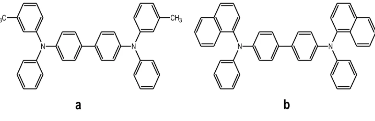
Hole Transport Materials have an important role in OLEDs device performance. Generally, triarylamine compounds have been used as hole-transport materials since the first fabrication of OLEDs in 1987. In lots of various triarylamine compounds N, N’-diphenyl-N, N’- bis(3-methyphenyl)-(1,1’-biphenyl)-4,4’- diamine (TPD) and N, N’-bis(1-napthalenyl) – N, N’ diphenyl)-(1,1’-biphenyl)-4,4’- diamine (NPB) are the most widely used as HTL materials in OLEDs. The chemical structure of these materials are shown in Figure 1.6 [16] [17].
N N CH3 C H3 N N
a
b
TPD and NPB are small molecules so that they can easily be evaporated under high vacuum. In addition, this material has lower energy barrier between HOMO energy levels of HTL and the work function of anode. A suitable HTM for electrophosphorence should also has high hole mobility. Since 𝑇𝑔 has an important role in high thermal and morphological stability [18] it should also satisfy high glass transition temperature (𝑇𝑔). The most used hole transport materials, TPD and NPB, have 65 ℃ and 95 ℃ 𝑇𝑔, respectively [19].
1.4.3 Electron transport and emissive materials (ETL and EM)
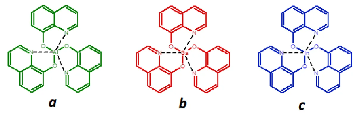
Emissive compounds are the most important materials in OLED devices, because recombination and light emitting occur in emissive layer. Generally, emissive materials (EL) show both electron transport and hole blocking properties.
Mobility of hole transport is about 2 or 3 orders of magnitude higher than electron mobility of electron transport. Hence, EMs should have both high electron mobility and good hole blocking property [20]. Tris-(8-hydroxyquinoline) aluminum (𝐀𝐥𝐪𝟑), tris-(8-hydroxyquinolinolato) gallium (𝐆𝐚𝐪𝟑) and tris-(8-hydroxyquinoline) indium (𝐈𝐧𝐪𝟑) materials are the most used emissive layer (EM) materials in OLED devices. The chemical structures of these materials are shown in Figure 1.7. Among these materials Alq3 is the most used ETL and EL because of its good thermal stability,
high electron affinity and ionization potential [21].
Figure 1.7 : Chemical Structures of Alq3 (a), Gaq3 (b) and Inq3 (c)
A recombination of holes and electrons occur between HTL and ETL. In addition, recombination region can be located in both ETL and HTL. If the recombination region is located in ETL, this layer behaves as the emissive layer (EM). If the
these devices are structured as successive layers of ITO/HTL/ETL(EM)/Metal or ITO/HTL(EM)/ETL/Metal. Besides, EM can also be coated as a separate layer. In that case, EM is neither in ETL nor in HTL therefore it is sandwiched between HTL and ETL (ITO/HTL/EM/ETL/Metal) [22].
1.4.4 Cathode materials
There must be charge balance between holes and electrons in injection to increase efficiency in OLEDs. As mentioned in previous parts, high barrier between organic layers and metals interface effect holes and electrons injection in a bad manner. In particular, barrier between organic layer and cathode electrode is too large compared to the barrier between organic layer and anode electrode [23, 24].
Unlike anode materials, cathode materials should have low work function. Mg, Ca, Li, Al and Ba are metals that satisfy low work function that are applicable to OLEDs [16]. Among these metals, Al is widely used as cathode material. In addition, LiF buffer layer can be used between Al cathode and organic layer, as well. This buffer layer increase the electron injection, device performance and also provides a longer lifetime [25]
1.5 Self-Assembled Monolayers
In literature, it is reported that indium tin oxide has been modified more than 20 years with several ways. Self-assembled monolayers (SAM) technique is one of the most used modification technique. This method firstly reported by Nuzzo and Allara and they published their study with the title as follows, “Absorption of Biofunctional Organic Disulfides on Gold Surface” in 1983[26]. Hence, Nuzzo and Allara are considered to be the pioneers of the SAMs.
Self-assembled monolayer technique is used to modify indium tin oxide in the literature to enhance hole injection and reduce the turn on voltage, as well [27]. In addition, SAMs have been used to enhance the interfacial compatibility between hydrophilic anode and hydrophobic HTL. Also, SAMs reported in literature as a current blocking layer or a moisture penetration blocking layer for OLEDs[28]. Because, pure adhesion between organic materials and inorganic electrodes is a big problem in OLED devices. This pure adhesion problem limit the performance and
smoothly bond with surface and changes the physical and chemical properties of surface although they are very thin layer. The thickness of this layer is about 2 or 3 nanometers. Such small scale makes SAM suitable for organic electronic and nano technological applications. In addition, they are easy to prepare and low cost, hence SAM materials have many applications in technology, such as protective coating, catalysts, biological sensors, optoelectronic devices etc. [30].
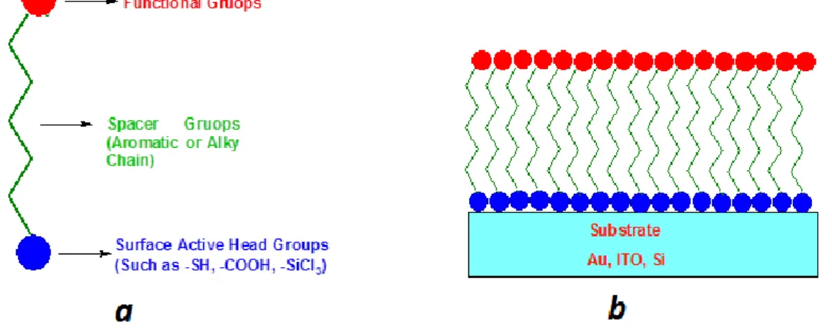
The Figure 1.8 SAM materials show the molecular structure of SAMs. As shown, it consists of three main parts; the first part is the surface-active head group, the second part is the spacer groups and the third part is the surface functional groups.
Figure 1.8 : Schematic illustration of SAMs (a) – Generation of SAMs on a substrate (b)
Surface-active head groups bond with surface spontaneously by strong or weak bonds. Also, surface active head groups provide the physical and chemical interaction on the active device layer. Spacer groups are aromatic or hetero-aromatic in structure. In addition, the spacer group determines the thickness of SAM. The last part, surface functional groups, determines the surface properties of SAMs. Besides, the functional group makes a new bond with the organic layer, such as hole transport layers.
Self-assembled monolayer molecules gradually bond on the surface in a definite period. Figure1.9 shows the increase of the SAM molecule amount with respect to time. As shown, after some time the amount of molecules accumulated on the surface of ITO saturates. Hence, the increase of accumulation by means of keeping ITO inside a SAM solution does not mean it will increase the performance of the
aggregation effects the device performance in a bad way. The best way to find the suitable time for reaching enough coating thickness is as follows; several ITO is kept inside the SAM solution for different periods of time. Then those several samples are evaluated with respect to their keeping time by means of their electrical device performance. Besides, as shown in the same figure, the coverage of SAM molecules achieves a saturation limit and become stable after a certain time.
Figure 1.9 : Surface coverage of SAM versus time [31]
1.6 OLED Efficiency
There are a few parameters to determine OLED efficiency. In this part External Quantum Efficiency (EQE), Internal Quantum Efficiency (IQE), current efficiency and power efficiency are explained briefly.
External quantum efficiency (ŋ𝒆𝒙𝒕) is the ratio of the number of photons emitted
from the surface of an OLED divided by the number of injected electrons. EQE also can be written as the ratio of the total number of photons which is emitted in all direction from the device[32]. The internal quantum efficiency (ŋ𝒊𝒏𝒕) is the ratio of the total number of photons generated within the organic layer to the number of
coupled out of structure into viewing direction (ŋ𝒄) [33]. By this definition, a relationship between EQE and IQE can be written as follows,
ŋ𝒆𝒙𝒕 = ŋ𝒊𝒏𝒕ŋ𝒄 (1.1)
Beside EQE and IQE, current efficiency (cd/A) and power efficiency (lm/W) are most used parameters for determining OLED device performance. For calculation of current and power efficiency of devices, luminance (cd/m2), voltage (V) and current (I) are used. Current efficiency (ŋ𝒄𝒆) is defined as emitting luminance per unit current[34]. In that case we define ŋ𝒄𝒆 as follows,
ŋ𝒄𝒆 = 𝑨𝑳/𝑰𝑶𝑳𝑬𝑫 (2.2)
Where L is the luminance of OLED, A is device active area and 𝑰𝑶𝑳𝑬𝑫 is driving current of the device. In addition to the current efficiency, power efficiency (ŋ𝒑)
depend on device voltage, current and luminance, as well. To attain high power efficiency, OLED device should emit high luminance with low current (I) and voltage (V) [35]. Hence ŋ𝒑 is defined as follows,
ŋ
𝒑=
𝑳
2. EXPERIMENTAL DETAILS
2.1 The Steps of OLED Preparation
The sequential manufacturing process of OLEDs is listed inFigure 2.1.
Figure 2.1 : Manufacturing process of OLEDs 2.2 Etching, Cleaning and Oxygen Plasma procedure for ITO
The first step of OLED fabrication was started with cutting the ITO coated glass. The surface resistivity of samples is about 18-24 Ω/sq. First of all ITO glass substrates were cut in a size of 1,5cm x 1,5cm by using a diamond pencil. After cutting process, ITO substrates were etched. Before start to etching, 1,1cm of ITO was covered with tape to prevent this part from the damage during the etching process. And then 0,4 cm ITO was etched by using king water (prepared with 3HCI and 1HNO3 acids) and
this length is defined as cathode. 0,4 cm of ITO substrates were etched to prevent short cut between anode and cathode.
Cutting of ITO (1,5cm x 1,5cm)
Etching of ITO substrate
Cleaning procedure of ITO
Oxygen Plasma procedure
Preparation of SAM solution and then plunge the ITO in this solution to grow SAM molecule on the ITO substrate
Coating organic layers (TPD and Alq3) and metal electrode (Al) with the thermal evaporation system
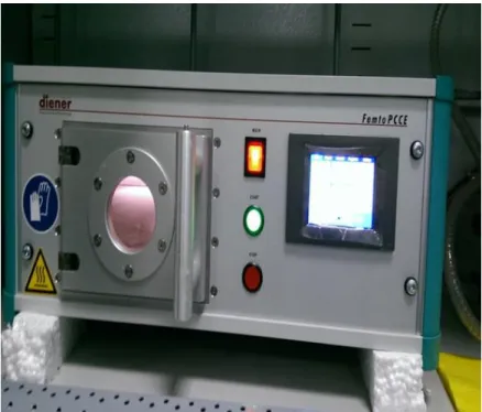
After etching, ITO substrates were cleaned and for this procedure ITO substrates were sonicated in deionized water, acetone and isopropanol respectively for 20 minutes. After cleaning procedure, all of the substrates were dried with nitrogen gas. Then, all of the samples are exposed to oxygen plasma for 8 minutes under vacuum. Oxygen plasma increases the work function of ITO and reduces the barrier for charge injection[36]. As shown in Figure 2.1 electronic diener femto PCCE was used as an oxygen plasma instrument.
Figure 2.2 : Oxygen Plasma Device 2.3 Surface Treatment of ITO by Using SAM Technique
In this study, two molecules (SAM materials) were designed and ITO substrates were modified with these SAM materials. It is believed that these molecules will increase charge injection and also solve the work function problem between the metal electrode (ITO) and organic layer. These molecules are also known as hole injection materials and which is called triphenylamine. Their chemical structures are shown in Figure 2.2 and their names are; 4,4''-bis(diphenylamino)-1,1':3',1''-terphenyl-5'-carboxylic acid (abbreviated as TPA in this thesis) and 4,4''-di-9H-carbazol-9-yl-1,1':3',1''-terphenyl-5'-carboxylic acid (abbreviated as CAR in this thesis). By modifying the ITO surface, the band gap between the Fermi energy level of ITO and HOMO energy level of organic material is expected to be decreased. Therefore,
the HOMO energy level of ITO/SAM surface should be determined with Cyclic Voltammetry after ITO was treated with SAM material.
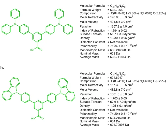
a. N N O O H Molecular Formula = C43H32N2O2 Formula Weight = 608.7265 Composition = C(84.84%) H(5.30%) N(4.60%) O(5.26%) Molar Refractivity = 190.05 ± 0.3 cm3 Molar Volume = 494.8 ± 3.0 cm3 Parachor = 1357.9 ± 4.0 cm3 Index of Refraction = 1.694 ± 0.02 Surface Tension = 56.7 ± 3.0 dyne/cm Density = 1.230 ± 0.06 g/cm3
Dielectric Constant = Not available Polarizability = 75.34 ± 0.5 10-24 cm3 Monoisotopic Mass = 608.246378 Da Nominal Mass = 608 Da Average Mass = 608.741874 Da b. N N O O H Molecular Formula = C43H28N2O2 Formula Weight = 604.6947 Composition = C(85.41%) H(4.67%) N(4.63%) O(5.29%) Molar Refractivity = 187.39 ± 0.5 cm3 Molar Volume = 482.8 ± 7.0 cm3 Parachor = 1301.0 ± 8.0 cm3 Index of Refraction = 1.703 ± 0.05 Surface Tension = 52.6 ± 7.0 dyne/cm Density = 1.25 ± 0.1 g/cm3
Dielectric Constant = Not available Polarizability = 74.29 ± 0.5 10-24cm3
Monoisotopic Mass = 604.215078 Da Nominal Mass = 604 Da Average Mass = 604.70997 Da
Figure 2.3 : Chemical structure of TPA (a) and CAR (b) Molecules
Each of these materials was solved in 10-3 M dimethyl sulfoxide solution. After dimethyl sulfoxide-SAMs solution was prepared, ITO substrates were kept in these solutions for 24 hours. After 24 hours passed, ITO substrates are rinsed with pure dimethyl sulfoxide to remove the residual SAM molecules which are not having strong bonding on the ITO surfaces. Then ITO substrates were dried with nitrogen (N2) gas and finally kept on the hot plate for 15 minutes at 80 0C (completely dry
ITO substrates).
2.4 Thermal Evaporation of Organic Layers and Metallic Layer
In this study, a thermal evaporation system (NANOVAK) was used for two different coating system. Namely, the system shown in Figure 2.2 is used to coat both organic
and metallic layers. In detail, one of the evaporation is made for small organic molecules like TPD, NPB, Alq3 etc.. The other evaporation is made for metallic
materials like Al, Ag, Au etc. Before starting evaporation, thickness monitors were calibrated and properties of both organic materials (TPD, Alq3) and metallic material
(Al) were entered. Evaporation procedure was completed under high vacuum (~4x10
-5
Torr) to have high quality thin layers.
TPD and Alq3 were coated on the SAM modified ITO substrates as HTL and EM,
respectively. After organic layers were coated, all of the samples were put into the glove box and cathode layer was coated with aluminum in this inert medium.
(a) (b)
Figure 2.4 : Organic (a) and Metallic (b) Evaporation Systems
In this study, six devices were fabricated with SAM materials and the effect of SAM materials was investigated on the electrical and optical characterization of OLED devices with compared to bare ITO OLED device and ITO:PEDOT:PSS OLED device. These device configurations are tabulated in Table 2.1.
Table 2.1 : Configuration of OLED devices Devices Transparent Anode SAM Materials PEDOT:PSS Hole Transport Layer Emissive Layer and ETL Cathode Layer Device 1 ITO - - TPD (~40nm) Alq3 (~40nm) Al (~100nm)
Device 2 ITO - PEDOT:PSS
TPD (~40nm) Alq3 (~40nm) Al (~100nm)
Device 3 ITO CAR -
TPD (~40nm) Alq3 (~40nm) Al (~100nm)
Device 4 ITO CAR PEDOT:PSS
TPD (~40nm) Alq3 (~40nm) Al (~100nm)
Device 5 ITO TPA -
TPD (~40nm) Alq3 (~40nm) Al (~100nm)
Device 6 ITO TPA PEDOT:PSS
TPD (~40nm) Alq3 (~40nm) Al (~100nm)
2.5 Characterization of OLED Devices
Surface topography and electrical characterizations of modified and unmodified ITO were determined by Atomic Force Microscopy (AFM) and Kelvin Probe Force Microscopy (KPFM). For surface topography, AFM was used with non-contact mode. For electrical characterization, KPFM was used with contact and non-contact
mode. Finally, for electrical and optical characterization, Keithley source meter, Labview software, Ocean optic and Spectrometer were used.
2.5.1 AFM surface characterization
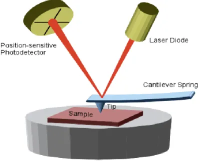
Atomic Force Microscope is the most effective instrument for taking nanoscale images of surface topography. In AFM devices usually piezoelectric materials are used as scanning probe because of their high resolution capabilities and fast response time [37].
The general work principle of AFM is illustrated in Figure 2.4. An AFM uses a cantilever with a very sharp tip to scan the sample surface. When cantilever approach to the surface, attractive force occurs between the surface and tip. This force deflects the cantilever. Cantilever deflection usually detected by a laser beam and this laser beam focuses on the top of the cantilever and directs to a position-sensitive photo diode[38]. All of the changes on the surface effect the cantilever deflection and accordingly position of laser change on the photo diode. This changing is recorded by a photo diode to determine surface image.
Figure 2.5 : General work principle of AFM (URL 2)
AFM devices usually include three modes. These modes are; contact, non-contact and tapping mode. Selections of these modes are determined according to the surface properties of materials. Generally, contact mode has been used for rigid materials, the non-contact mode has been used for soft materials and tapping mode has been
used for both rigid and soft materials. In addition, the main goal of AFM is determine 3D surface view, lithography and surface roughness [CAN M. 2012].
In this study, Nanosurf flex AFM was used to investigate the surface topography of modified and unmodified ITO. The non-contact mode was used for both of the modified and unmodified ITO measurements. The Figure 2.5 shows Nanosurf flex AFM device and its software screen.
Figure 2.6 : Nanosurf Flex AFM (right) and its software (left) 2.5.2 Kelvin probe force microscopy (KPFM) surface characterization
Kelvin Probe Force Microscopy is usually used to image surface potential difference between the samples and probes. Also it gives details about surface fotovoltage of the semiconductors[39]. Thus, it gives information about the work function of conductive thin films.
In KPFM method two conductors have been used as parallel plate capacitor. The contact potential difference between (VCPD) of two materials are defined as in
Equation 2.1.
𝑉𝐶𝑃𝐷 = 1
𝑒(∅2−∅1) (2.1) Where ∅2 and ∅1 are work function of conductors. Due to the distance between parallel plate capacitor, a periodic vibration of distance (ω) is occurred. This vibration causes a current and this current equation is written as follows,
𝑖(𝑡) = 𝑉𝐶𝑃𝐷𝜔𝛥𝐶𝑐𝑜𝑠𝜔𝑡 (2.2)
In this study, Ntegra Solaris (NT-MDT) KPFM was used to determine the surface potential difference between the modified and unmodified ITO.
2.5.3 Cyclic voltammetry characterization
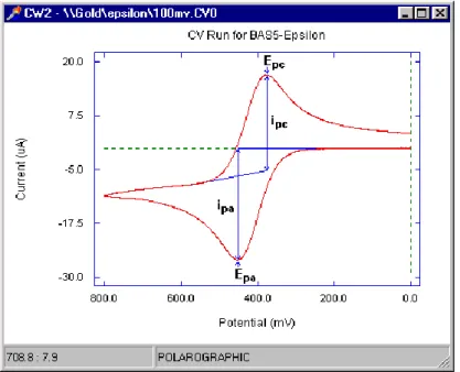
Cyclic Voltammetry (CV) is used in electrochemistry, inorganic chemistry, organic chemistry and biochemistry. It consists of cycling the potential of an electrode. This electrode dips in a solution and measures the current. The potential of this working electrode is controlled by a reference electrode. Silver (Ag) or silver chloride (AgCI) usually used as reference electrode [41].
The potential is applied between the working electrode and the reference electrode. Where, the current is measured between the working electrode and the counter electrode. These data gives current versus applied potential graph. This graph is referred as voltammogram. The Figure 2.6 shows a current versus potential voltammogram.
Figure 2.7 : Typical current vs potential graph of CV 2.5.4 Contact angle characterization
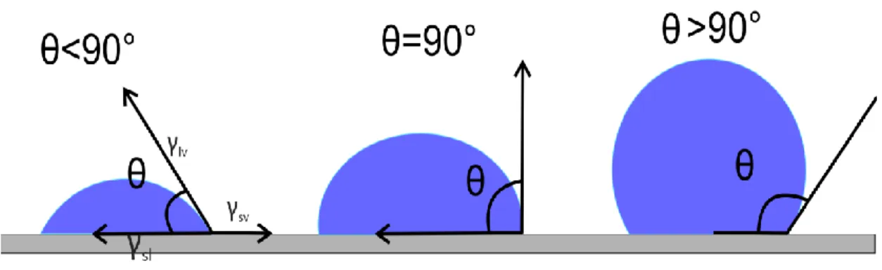
The contact angle measurement technique is usually used to determine whether a solid surface is hydrophobic or hydrophilic. Generally, this is explained as follows. If a contact angle is less than 90o, solid surface is considered as hydrophilic and the fluid is spread over a large area of surface. If the contact angle is larger than 90o it
surface[42]. The Figure 2.7 shows that if the liquid spreads on the surface, a small contact angle is observed. If the liquid beads on surface, a large contact angle is observed.
Figure 2.8 : Illustration of contact angles on a smooth solid surface.
Generally, measurement of contact angles on a solid surface is the easiest way to determine the surface energetics (solid-vapor and solid-liquid surface tensions). It is obtained by Young’s equation as follows,
𝛾𝑙𝑣cos 𝛳 = 𝛾𝑠𝑣 − 𝛾𝑠𝑙 (2.3)
where 𝜭, 𝛾𝑙𝑣 , 𝛾𝑠𝑣 and 𝛾𝑠𝑙 are Young contact angle, liquid-vapor surface tension, solid-vapor surface tension and solid- liquid surface tension, respectively[43].
2.5.5. Optical and electrical characterization
To obtain current-voltage (I-V) characteristic of OLED devices, Keithley 2400 source meter was used. Voltage was applied between the anode and cathode with two probes of Keithley source meter and LabView software was used to obtain I-V characteristic of OLED on a computer screen.
In order to obtain optical properties of OLED devices QE6500 spectrometer was used.
3. RESULT AND DISCUSSION
PEDOT:PSS which is coated on ITO has been used most effective hole injection material in organic light emitting diode. But according to many researches, ITO/PEDOT:PSS interface is not stable and some degradation has been occurred on ITO surface. The degradation reason of ITO can be explained by etching of ITO due to the strong acidic nature of PEDOT:PSS. Because it is known that ITO is very sensitive to acidic environments and therefore it influences device life time negatively[44, 45]. Because of this problem self-assembled monolayers was used which is an alternative material as hole injection layer instead of PEDOT:PSS. In addition, the effect of self-assembled monolayer on OLEDs device was discussed in the preceding parts.
This chapter includes six parts and in these parts; electrical, optical and surface characterization of modified and unmodified ITO was analyzed. In the first three section modified ITO with SAM materials were compared to unmodified ITO and modified ITO with PEDOT:PSS via theirs electrical and optical characterization. In the fourth part, surface characterization of modified and unmodified ITO was performed with AFM and KPFM. In the fifth part, electrical characterization of SAM materials (CAR-TPA) was analyzed with Cyclic Voltammetry and in the last part, modified and unmodified ITO surface was analyzed with contact angle measurement.
3.1 Electrical and Optical Characterization Results 3.1.1 Cycle voltammetry results
In this study, CH instruments CHI440B cyclic Voltammetry was used to determine the electrochemical behavior of SAM (TPA-CAR) materials. Modified ITO with SAM materials, platinum wire and silver (Ag) were used as working electrode, counter electrode and a reference electrode respectively. Before starting the measuring process, nitrogen gas has been used to remove oxygen from the electrolyte.
The Figure 3.1 and Figure 3.2 show CV voltammogram of ‘TPA and CAR’ SAM materials. The energy level of EHOMO was found from the inflection point of these
graphs by using Equation 3.2. Using Equation 3.1 and Equation 3.2 values of ELUMO
and EHOMO can be calculated.
Figure 3.1 : CV Voltammogram of modified ITO with TPA
ELUMO = e( E1/2(ind.) + 4,4) (3.1)
EHOMO = e( E1/2(yük.) + 4,4) (3.2)
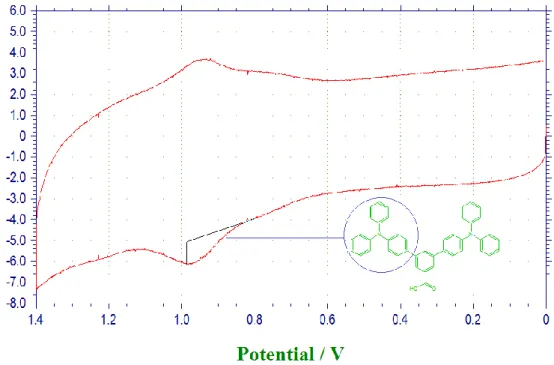
As shown in Figure 3.1 and Figure 3.2 reversible oxidation of TPA and semi reversible oxidation of CAR was determined 0,92 V and 1,18 V, respectively. HOMO energy level of TPA and CAR were calculated using Equation 3.2. This energy level was founded as -5,32 eV and -5,58 eV for TPA and CAR, respectively. The effect of SAM materials on the ITO surface can be seen in the energy diagram of devices given in Figure 3.3. As it will be understood from the figure both TPA and CAR increase the energy level of ITO. Nevertheless, TPA is more suitable for ITO and TPD, because it makes an energy step between the ITO and TPD. Therefore, devices which are modified with TPA should have better electrical and optical results.
(a) (b)
Figure 3.3 : Energy diagram of OLED devices with TPA (a) and CAR (b) 3.1.2 Electrical and optical characterization of 4,4''-di-9H-carbazol-9-yl-1,1':3',1''-terphenyl-5'-carboxylic acid (CAR)
To determine the effect of ITO surface treatment on OLED device performance, six different device structures were prepared. Then, the manufactured OLEDs are compared via their electrical and optical properties. In this section, ITO was
devices (ITO/CAR and ITO/CAR/PEDOT:PSS) were compared with reference devices (Bare ITO and ITO/PEDOT:PSS). Detailed device numbers and structures are given in Table 3.1.
Table 3.1 : Device numbers and their structures
Device 1 Device 2 Device 3 Device 4
ITO/TPD/Al q3/Al ITO/PEDOT:PSS/TP D/Alq3/Al ITO/CAR/TPD/ Alq3/Al ITO/CAR/PEDOT:PSS/T PD/Alq3/Al
I-V characteristic curves show the relationship between the current flowing through the electronic device and applied voltage across its terminals. It is the most important electrical property for an organic light emitting diode. By means of this characterization, one can determine if really a diode is manufactured or not. The Figure 3.4 shows J-V curves of Device 1,2,3 and 4. As known, semiconductor diodes begin conducting electricity only if a certain threshold voltage or cut-in voltage is present in forward bias and we expect to see this behavior in J-V graph.
5 6 7 8 9 10 11 12 13 14 15 16 17 0 500 1000 1500 2000 2500 3000 3500 4000 4500 C urrent D en sit y (A /m 2 ) Voltage (V) Device 1 Device 2 Device 3 Device 4
The Figure 3.4 shows a perfect I-V diode characteristic. Device 1,2 and 3 are not conducting electricity until they are applied ~8,2 volts and ~12,5 volts for Device 4. After ~8,2 and ~12,5 volts is applied, devices start to conduct electricity. We refer that voltages (8,2 and 12,5) as a turn on voltage. In Device 1,2 and 3 modified ITO was used and these devices show a low turn on voltage compared to Device 4 which uses a bare ITO. The detailed structure of all devices can be seen in Table 3.1. In OLEDs, electrical energy is converted into optical energy. This feature shows there is a direct relationship between the voltage-current and luminance. In addition, this means that the luminance has a key point for optical properties of OLEDs. The Figure 3.5 shows luminance change versus voltage of Device 1 to 4.
7 8 9 10 11 12 13 14 15 16 0 200 400 600 800 1000 1200 Lu mi na nc e (cd /m 2 ) Voltage (V) Device 1 Device 2 Device 3 Device 4
Figure 3.5 : Luminance versus Voltage graph of Device 1 to 4
If Figure 3.4 and Figure 3.5 clearly compares, the relationship between electrical and optical behavior of OLEDs. In Figure 3.4 turn on voltage of Device 1, 2 and 3 are about 8,2 V and Device 4 is about 12,5 V. In the same way Device 1,2,3, and 4 gives the luminance at the same turn on voltage (Figure 3.5). As expected, Device 2 with ITO/PEDOT:PSS has maximum luminance, Device 3 and 4 with ITO/CAR and ITO/CAR/PEDOT:PSS show good performance according to Device 1. As can be
seen in Figure 3.4 and Figure 3.5 CAR material has good result on device performance. Because, it is solved the contact problem between ITO electrode and organic layers.
After current, voltage and luminance of devices are determined, the efficiency of OLED devices can be calculated. Figure 3.6 and figure 3.7 show current and power efficiency of device 1,2,3 and 4, respectively. Here, current efficiency is convenient for quantifying the properties of OLEDs for display applications and Power efficiency is the ratio luminous power emitted in the forward direction[33].
100 200 300 400 500 600 700 800 900 1000 1100 0,1 0,2 0,3 0,4 0,5 0,6 0,7 C urrent E ff icienc y (A /m 2 ) Luminance (cd/m2) Device 1 Device 2 Device 3 Device 4
100 200 300 400 500 600 700 800 900 1000 1100 0 1000 2000 3000 4000 5000 6000 P ower E ff icienc y ( lm/ W) Luminance (cd/m2) Device 1 Device 2 Device 3 Device 4
Figure 3.7 : Power Efficiency vs Luminance graph of Device 1 to 4
The Figure 3.8 shows the intensity (a.u) versus wavelength (nm) graph. As can be seen in the figure, all devices emit light almost at the same wavelength. In addition, all devices have maximum intensity at the same wavelength. It means that, recombination of electrons and holes were occurred in emissive layer.
300 400 500 600 700 800 900 0 5000 10000 15000 20000 25000 30000 35000 Intens it y ( a.u) Wavelength (nm) Device 1 Device 2 Device 3 Device 4
Figure 3.8 : Intensity vs Wavelength graph for Device 1 to 4
Table 3.2 : Electrical and Optical details about devices Turn on Vol. (V) Max. Lum. (cd/m2) Max. Current Effi. (cd/A) Max. Power Effi. (lm/W) Device 1 12,5 250,7 0,211 1753 Device 2 8,0 1111,5 0,636 5702 Device 3 8,2 458,6 0,426 3166 Device 4 8,1 776,4 0,466 4211
3.1.3 Electrical and optical characterization of 4,4''-bis(diphenylamino)-1,1':3',1''-terphenyl-5'-carboxylic acid (TPA)
In this section, four different devices were prepared and the corresponding structures and their abbreviated names are tabulated in Table 3.3.
Table 3.3: Device structures and their numbers
Device 1 Device 2 Device 5 Device 6
ITO/TPD/Al q3/Al ITO/PEDOT:PSS/TP D/Alq3/Al ITO/TPA/TPD/ Alq3/Al ITO/TPA/PEDOT:PSS/T PD/Alq3/Al
As can be seen in Table 3.3 ITO was modified with TPA and TPA/PEDOT:PSS for Device 5 and Device 6, respectively. These devices were compared to reference devices (Device 1 and Device 2) via their electrical and optical characterization. In the previous section, the electrical and optical characterization of OLED device was explained. Hence, brief information is given in the related graphs. First of all, current-voltage and luminance-voltage graphs and then current, power efficiency and intensity versus wavelength graphs are given in Figure 3.9, Figure 3.10, Figure 3.11, Figure 3.12 and Figure 3.13, respectively.
6 7 8 9 10 11 12 13 14 15 16 17 0 500 1000 1500 2000 2500 3000 3500 4000 C urrent D en sit y (A /m 2 ) Voltage (V) Device 1 Device 2 Device 5 Device 6
As can be seen in Figure 3.9, Device 5 and Device 6 have the same turn on voltage with reference Device 2 and also they show a good performance with respect to reference Device 1. Also, Figure 3.9 (electrical characterization) and Figure 3.10 (optical characterization) shows similar features.
6 7 8 9 10 11 12 13 14 15 16 0 200 400 600 800 1000 1200 1400 Lu mi na nc e (cd /m 2 )
Voltage (V)
Device 1 Device 2 Device 5 Device 6200 400 600 800 1000 1200 1400 0,0 0,1 0,2 0,3 0,4 0,5 0,6 0,7 0,8 C urrent E ff icienc y ( cd /A ) Luminance (cd/m2) Device 1 Device 2 Device 5 Device 6
Figure 3.11 : Current Efficiency versus Luminance graph
200 400 600 800 1000 1200 1400 0 1000 2000 3000 4000 5000 6000 7000 8000 P ower E ff icienc y ( lm/ W) Luminance (cd/m2) Device 1 Device 2 Device 5 Device 6
300 400 500 600 700 800 900 0 5000 10000 15000 20000 25000 30000 35000 40000 45000 50000 Intens it y ( a.u) Wavelength (nm) Device 1 Device 2 Device 5 Device 6
Figure 3.13 : Intensity versus Wavelength Graph
Table 3.4 : Electrical and Optical details about devices. Turn on Vol. (V) Max. Lum. (cd/m2) Max. Current Effi. (cd/A) Max. Power Effi. (lm/W) Device 1 12,5 250,7 0,211 1753 Device 2 8,0 1111,5 0,636 5702 Device 5 8.3 558,5 0,575 4175 Device 6 8,0 1443 0,696 6678
3.1.4 Electrical and optical characterization of ‘TPA and CAR’ materials
In this part, also the last part of electrical and optical characterization, all of the devices were compared with each other. In the previous section (Section 3.1.2 and 3.1.3.), we compared devices which include CAR and TPA treated ITO with reference devices (Device 1 and Device 2). In this section, the devices which are fabricated with SAM (CAR-TPA) treated ITO were compared with reference devices
and also they are compared with each other, again. Device numbers and structures were given in table 3.5.
Table 3.5 : Device numbers and structures Device Numbers Device Structures Device Numbers Device Structures
Device 1 ITO/TPD/Alq3/Al Device 4 ITO/CAR/PEDOT:PSS/TPD/Alq3 /Al
Device 2 ITO/PEDOT:PSS/TPD/Alq3
/Al Device 5 ITO/TPA/TPD/Alq3/Al
Device 3 ITO/CAR/TPD/Alq3/Al Device 6 ITO/TPA/PEDOT:PSS/TPD/Alq3/ Al
In section 3.1.1 HOMO level of TPA and CAR was found with cyclic Voltammetry. According to CV results, Device 5 which is modified with TPA should show better performance than Device 3. Because Device 3 includes modified ITO with CAR and its HOMO energy level (Figure 3.3) is not as suitable as a TPA HOMO energy level for ITO and TPD.
SAM materials may not be completely covered on the ITO surfaces. Therefore, PEDOT:PSS was coated on TPA and CAR (Device 4 and Device 6) to observe changing in device performance and observing stability of SAM materials. As expected, Device 4 and Device 6 show better performance than Device 3 and Device 5. This performance change can be seen in Figure 3.14, Figure 3.15, Figure 3.16, Figure 3.17 and Figure 3.18 where the electrical and optical behavior of devices are compared from these graphics, it can be seen that all devices are compatible with each other.
6 7 8 9 10 11 12 13 14 15 16 17 0 500 1000 1500 2000 2500 3000 3500 4000 C urrent D en sit y (A /m 2 ) Voltage (V) Device 1 Device 2 Device 3 Device 4 Device 5 Device 6
Figure 3.14 : Current Density versus Voltage graph
6 7 8 9 10 11 12 13 14 15 16 0 200 400 600 800 1000 1200 1400 Lu mi na nc e (cd /m 2 ) Voltage (V) Device 1 Device 2 Device 3 Device 5 Device 4 Device 6
200 400 600 800 1000 1200 1400 0,0 0,1 0,2 0,3 0,4 0,5 0,6 0,7 0,8 C urrent E ff icienc y ( cd /A ) Luminance (cd/m2) Device 1 Device 2 Device 3 Device 5 Device 4 Device 6
Figure 3.16 : Current Efficiency versus Luminance graph
200 400 600 800 1000 1200 1400 1600 1000 2000 3000 4000 5000 6000 7000 P ower E ff icienc y ( lm/ W) Luminance (cd/m2) Device 1 Device 2 Device 3 Device 5 Device 4 Device 6
300 400 500 600 700 800 900 0 5000 10000 15000 20000 25000 30000 35000 40000 45000 50000 intens it y ( a.u) Wavelength (nm) Device 1 Device 2 Device 3 Device 4 Device 5 Device 6
Figure 3.18 : Intensity versus Wavelength graph
Table 3.6 : Electrical and Optical details about devices Turn on Vol. (V) Max. Lum. (cd/m2) Max. Current Effi. (cd/A) Max. Power Effi. (lm/W) Device 1 12,5 250,7 0,211 1753 Device 2 8,0 1111,5 0,636 5702 Device 3 8,2 458,6 0,426 3166 Device 4 8,1 776,4 0,466 4211 Device 5 8.3 558,5 0,575 4175 Device 6 8,0 1443 0,696 6678
3.2 Surface Characterization Results 3.2.1 Atomic force microscope results
The surface topography of modified and unmodified ITO was characterized by AFM and the AFM images were shown in figure 3.19. As it is widely known, SAM materials have nanoscale size, hence it is too difficult to observe them on ITO surface. However, surface roughness (RMS) measurement differences will give some information about modification of ITO surface with TPA and CAR SAM materials. The results of surface roughness are given in Table 3.7.
(a) (b)
(c) (d)
Figure 3.19 : AFM images of Bare ITO (a), modified ITO with CAR (b) and TPA (c). After organic materials coating on ITO (d)
Table 3.7 : Surface roughness of Bare ITO, ITO/CAR, ITO/TPA and ITO/TPD/Alq3
Bare ITO ITO/CAR ITO/TPA ITO/TPD/Alq3
Unmodified ITO has a higher surface roughness than modified ITO with CAR and TPA. It can be said that, SAM materials were covered on ITO surface and filling the vacancies or holes. That process decreases the roughness of ITO.
3.2.2 Kelvin probe force microscope results
In order to determine the surface potential of modified and unmodified ITO Kelvin Probe Force Microscope was used. With this technique, we obtained surface topography images and surface potential topography images. These images are shown as in following Figure 3.20, Figure 3.21 and Figure 3.22.
(a) (b)
Figure 3.20: AFM topography (a) and surface potential (b) of bare ITO with KPFM technique.
(a) (b)
Figure 3.21 : AFM topography (a) and surface potential (b) of ITO/CAR with KPFM technique
(a) (b)
Figure 3.22 : AFM topography (a) and surface potential (b) of ITO/TPA with KPFM technique
The Figure 3.20 shows the surface potential of bare ITO and modified ITO with CAR and TPA results which is measured with KPFM.
-1,0 -0,5 0,0 0,5 1,0 1 2 3 4 5 6 7 Ma g (n A ) Voltage(V) Bare(ITO)
-1,5 -1,0 -0,5 0,0 0,5 1,0 1,5 0 1 2 3 4 5 6 7 8 9 10 Ma g (n A ) Voltage (V) ITO/CAR
Figure 3.24 : Surface Potential of ITO/CAR
-1,0 -0,5 0,0 0,5 1,0 1,5 0 1 2 3 4 5 6 7 8 9 M ag ( nA ) Voltage(V) ITO/TPA
Figure 3.25 : Surface Potential of ITO/TPA
The surface potential of bare ITO, ITO/CAR and ITO/TPA were measured as 0,113 mV, 0,211 mV and 0,216 mV respectively. KPFM results show that, CAR and TPA materials increased the surface potential of ITO. It means that the work function of
ITO/CAR and ITO/TPA surface close to the HOMO level of TPD, which shows it will increase the hole injection from ITO to TPD.
Table 3.8 shows the surface potential values of modified and unmodified ITO. Table 3.8 : Surface potential of Bare ITO and modified ITO with CAR and TPA
Bare ITO ITO/CAR ITO/TPA
Surface
Potential ~ 0,113 mV ~ 0,211 mV ~ 0,216 mV
3.2.3 Contact angle results
As known, ITO has a hydrophilic surface and when a fluid contact with ITO surface, it is spread over a large area of surface. In this study, distilled water was used as fluid. Figure 3.24 shows the contact angle of bare ITO, ITO/CAR and ITO/TPA surface. As seen in this figure, modified ITO has a larger contact angle according to bare ITO. Because, TPA and CAR molecules make a barrier between ITO and fluid.
4. CONCLUSIONS
Indium thin oxide (ITO) has been widely used as anode materials in OLED devices because of its high conductivity (~104 s/cm), high transparency (~90% at visible
range) and high work function (~4,7 eV) [36]. In OLED devices, ITO is direct contact with organic layer, but the work function of metal electrode (ITO) and energy level of organic materials have large injection barrier. This barrier lead to poor charge injection and low efficiency[29]. In this thesis, we focused on solving this problem and to solve this problem ITO substrates were modified with SAM materials to increase HOMO energy level of ITO. SAM materials are one of the most promising techniques to modify ITO surface due to its ease of processing and low cost. In this study, TPA and CAR materials were used as SAM materials. After ITO was modified with SAM materials, OLED device performance was increased with respect to the reference devices, which also includes bare ITO.
In Chapter 1, brief information was given about organic light emitting diode, its historical development and its application area. Then the device structure of OLEDs was explained. After the device structure was given, principle of OLEDs operation was explained with charge injection. And then anode materials, cathode materials, hole transport materials, electron transport, and emissive materials were given. In addition, SAM material properties and its techniques were given. Finally, OLEDs efficiency was explained.
In chapter 2 experiment details was given. Firstly, the step of OLED preparation was determined. Then, etching procedure, cleaning procedure and oxygen plasma procedure of ITO substrates was explained. After that surface treatment of ITO with SAM molecules was given. Afterwards, thermal evaporation of organic and metallic layer and also device configuration of OLED devices were explained. Finally, AFM surface characterization, KPFM surface characterization, cyclic Voltammetry characterization, contact angle characterization and electrical and optical characterization were explained.
![Figure 1.5 : OLED structure with the hole and electron blocking layers [11].](https://thumb-eu.123doks.com/thumbv2/9libnet/3711645.24985/18.892.221.712.683.1016/figure-oled-structure-hole-electron-blocking-layers.webp)