Contents lists available atScienceDirect
Materials Science in Semiconductor Processing
journal homepage:www.elsevier.com/locate/msspSynthesis and characterization of CdS window layers for PbS thin film solar
cells
Fatma Göde
⁎, Serdar Ünlü
Department of Physics, Faculty of Arts and Science, Burdur Mehmet Akif Ersoy University, 15030 Burdur, Turkey
A R T I C L E I N F O Keywords:
CdS Thin films Solar cells
Chemical bath deposition
Successive ionic layer adsorption and reaction
A B S T R A C T
Window layers, cadmium sulfide (CdS) thin films were synthesized on tin doped indium oxide coated glass substrates (ITO) with two different temperatures of 85 °C and 90 °C and ammonium hydroxide concentration of 1 M and 9.96 M, respectively via the chemical bath deposition (CBD) method, while absorption layers, lead sulfide (PbS) thin film were deposited on ITO substrates at room temperature using the successive ionic layer absorption and reaction (SILAR) technique. Then, these layers were integrated in ITO/CdS/PbS/Ag solar cell structures. The structural, morphological and optical properties of the thin films as well as electrical properties of the solar cells were investigated. X-ray diffraction studies showed that the CdS thin films have hezagonal structure while PbS thin films have cubic structure. The photovoltaic performance of the solar cells showed that the solar cell fabricated with CdS film deposited at 90 °C exhibited higher efficiency ( ) of 4.85% including JSC = 12.44 mA cm−2, VOC= 1 V, FF = 0.39 than the CdS film deposited at 85 °C ( = 3.59%, JSC= 9.43 mA cm−2,
VOC= 1 V, FF = 0.38. These results reveal that the crystal structure, surface morphology and optical properties of CdS thin film have a significiant effect on device performance and the solar cell fabricated using CdS film deposited at 90 °C shows better photovoltaic performance.
1. Introduction
The development of low-cost polycrystalline thin film solar cell devices is important for future energy generation. The chemical bath deposition (CBD) and successive ionic layer absorption and reaction (SILAR) techniques have been more attractive technologies which are well suited for large area coating, low temperature processing, simple, economical and energy-efficient methods for preparing thin films of chalcogenide semiconductors [1–5] such as cadmium sulfide (CdS), lead sulfide (PbS), cadmium tellur (CdTe) and cadmium selenide (CdSe) compared with other expensive techniques that need vacuum technol-ogies such as molecular beam epitaxy, atomic layer deposition and vacuum evaporation, etc. The CdS and PbS materials have been chosen in order to enhance solar energy conversion from ultraviolet region to the near infrared (NIR) spectral region. These materials belonging to the II–VI group have suitable direct band gaps (CdS = 2.28–2.45 eV[1] and PbS = 0.41 eV) and in solar energy conversion. CdS and PbS layers are used as window and absorber materials, respectively[6–11]in solar cells.
The CdS film surface has a crucial role in photovoltaic properties of the solar cells. The selection of precursor solution is one of the most important factors in determining the properties of CdS films such as
film thickness, crystallinity, grain size, surface roughness and elemental composition. Beside of the cadmium ion source, complex agents such as ammonia [1,12], ammonium sulphate [13], ammonium hydroxide [14], triethanolamine[15], tartaric acid[16], etc. play a crucial role in nucleation and growth. Complex agents are used for shape control of semiconductors and the surface properties including surface roughness and grains of the thin film have a great influence on solar cell con-version efficiency. In our previous work[1], we showed that the shape and grain size of the CdS nanoparticles can be controlled by changing ammonia concentration. Mir et al. [17]showed that complex agent (ethanolamine, ethylenediamine, mercaptoethanol, 1,3-Diaminopro-pane, and 2,2-dimethylpropylenediamine) has a critical effect on im-proving surface properties of CdS/TiO2 film and its photovoltaic
properties. Patil et al.[18]investigated the effect of complexing agent on the photoelectrochemical properties of CdS thin films. They found out that the existence of triethanolamine complex led to a better crys-tallinity and marigold flower-like morphology. As a result, the im-proved crystallinity and surface area led to enhanced optical absorp-tion, the short circuit current density, as well as, open circuit voltage which in turn increased conversion efficiency.
In this work, in order to obtain thin film solar cell structures of ITO/ CdS/PbS/Ag, window (CdS) and absorption (PbS) layers were
https://doi.org/10.1016/j.mssp.2018.10.011
Received 4 July 2018; Received in revised form 7 September 2018; Accepted 10 October 2018
⁎Corresponding author.
E-mail address:[email protected](F. Göde).
sequentially synthesized on ITO substrates by means of the CBD and SILAR methods, respectively. CdS thin films were produced at two different deposition temperature of 85 °C and 90 °C using two different ammonium hydroxide concentration as 1 M and 9.96 M, respectively. Hence, we have fabricated two solar cells. The reason of using two different ammonium hydroxide concentration in CdS film is to see the effect of ammonium hydroxide on solar cell performance. It should be noted that the effect of ammonium hydroxide on solar cell performance is firstly investigated in the present work.
2. Experimental
2.1. Synthesize of CdS thin films
The CBD method was used for the deposition of CdS thin films on tin doped indium oxide coated glass substrates (ITO) with sheet resistances changing between 10 Ω/sq and 15 Ω/sq (76 mm × 26 mm × 1 mm) at room temperature (30 °C). Before deposition, the ITO substrates were washed by detergent, boiled in ultrapure water and cleaned in me-thanol, acetone and ultrapure water (18.2 MΩ cm) for 15 min sequen-tially. Cadmium nitrate [(CdN2O6·4H2O); MA= 308.48 g/mol; ≥ 99%
purity; Sigma Aldrich mark] and thiourea [(NH2CSNH2);
MA= 76.12 g/mol; ≥ 98% purity; Merck mark] were used as the source of Cd2+ and S2-ions, respectively. The CdS thin films were
synthesized from 30 ml of 0.1 M cadmium nitrate, 12 ml of 1 M tri-so-dium citrate (TSS) [(C6H5Na3O75,5H2O); MA= 357,16 g/mol; ≥ 99%
purity; Merck mark], 30 ml of 1 M and 9.96 M ammonium hydroxide [(NH4OH); 25% purity; Merck mark] and 10 ml of 1 M thiourea. Then,
the rest of the solution was completed to 100 ml by adding ultrapure water. In this experiment, tri-sodium citrate and ammonium hydroxide were added into the solution to make a complex with metal ions. ITO substrates were dipped into the beakers containing different tempera-tures 85 °C and 90 °C with different ammonium hydroxide quantities 1 M and 9.96 M, respectively. The beakers were kept in a water bath maintained at 85 °C and 90 °C and the films were waited for 2 h. After deposition, the CdS films were rinsed with ultrapure water and dried in air. The deposition of CdS films was based on the slow release of Cd2+
and S2−ions in the solution, which are then condensed onto ITO
sub-strates. At the end of these experiments, we produced two CdS films: one is deposited at 85 °C using 1 M ammonium hydroxide and other is deposited at 90 °C using 9.96 M ammonium hydroxide.
2.2. Synthesize of PbS thin films
The SILAR method was used for the deposition of PbS thin films onto ITO substrates at room temperature (30 °C). This technique is a versatile method for the deposition of PbS thin films on to glass sub-strates [3]. In order to obtain PbS thin film, ITO substrate was im-mersed into a cation precursor solution for 20 s, containing 20 ml of 0.05 M lead acetate [(CH3COO)2Pb 3H2O); MA= 379.34 g/mol;
99.5–102.0% purity; Merck mark], and 5 ml of 1.5 M NH4OH, and then,
it was rinsed with ultrapure water for 40 s before it was immersed into
Table 1
Preparative parameters of solar cells.
Solar cells CBD deposited CdS thin films SILAR deposited PbS thin film Cd2+(M) S2–(M) NH
4OH (M) Temperature(°C) Pb2+(M) S2–(M) Dipping time (s) Rinsing time (s) SILAR cycle
A 0.1 1 1 85 0.05 0,06 20 40 20
B 0.1 1 9.96 90
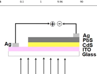
Fig. 1. Shematic illustration of the ITO/CdS/PbS/Ag solar cell.
an anion solution containing 25 ml of 0.06 M thioacetamide (TA) [(CH3CSNH2); ACS, Reag. Ph Eur.] for additional 20 s. The substrate
was rinsed again with ultrapure water for 40 s to remove the unreacted ions. By repeating above SILAR steps 20 times, PbS thin film was de-posited onto ITO and ITO/CdS substrates.
2.3. Formation of ITO/CdS/PbS/Ag solar cells
The CdS thin films were synthesized with two different tempera-tures and two different molarity of NH4OH on ITO substrates as shown
inTable 1. In order to produce solar cells, the CdS and PbS thin films are deposited sequentially on ITO substrates by the CBD and the SILAR methods, respectively.Fig. 1shows the structure of the solar cells with
silver contact made by hand using silver past. Fabricated solar cells are labeled as follows: A-ITO/CdS/PbS (85 °C; 1 M NH4OH), B-ITO/CdS/
PbS (90 C; 9.96 M NH4OH).
Efficiency ( ) is the most important parameter to make a comment on the performance of a solar cell, which is determined by both short-circuit current density (JSC) and open-circuit voltage (Voc) via the fol-lowing relation:
Table 2
Structural properties of CdS and PbS thin films.
Material T (°C) Observed values Standard values (hkl) JCPDS
2θ (°) d (Å) 2θ (°) d (Å) I(f) ITO/CdS 85 25.04 3.553 24.81 3.586 62.0 (100) 41-1049 26.07 3.415 26.51 3.360 91.0 (002) 41-1049 28.31 3.150 28.18 3.164 100.0 (101) 41-1049 43.09 2.097 43.68 2.071 48.0 (110) 41-1049 ITO/CdS 90 25.18 3.534 24.81 3.586 62.0 (100) 41-1049 26.67 3.339 26.51 3.360 91.0 (002) 41-1049 44.03 2.055 43.68 2.071 48.0 (110) 41-1049 52.25 1.749 52.80 1.733 15.0 (201) 41-1049 ITO/PbS 30 26.13 3.407 25.96 3.429 84 (111) 05-0592 30.19 2.958 30.08 2.969 100 (200) 05-0592 43.03 2.100 43.06 2.099 57 (220) 05-0592 50.61 1.802 50.98 1.790 35 (311) 05-0592
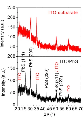
Fig. 3. X-ray diffraction patterns of PbS thin film.
= FFV J P
oc sc
in (1)
wherePinis the incident power and FF is the fill factor obtained using the following equation:
=
FF V I
V J
m m
oc sc (2)
where V Im mis the maximum power point of the product of the voltage and the current[19].
2.4. Characterization
XRD measurements were performed on a Bruker A8 advanced dif-fractometer with Cu Kα(0.154 nm) radiation. The surface morphology
of the thin films and solar cells were investigated using EVO40-LEO scanning electron microscopy (SEM) and a park system XEI Atomic Force Microscope (AFM) in non-contact mode. The absorption spectra were measured by using a UV–Vis spectrophotometer (PG-T60) in the wavelength of 300–1100 nm. The photovoltaic performance of the solar cells was obtained from current (I-V) voltage measurements under sunlight at mid-day and after lightining for 2 h with 7 W white led lamp by a computer-controlled Keithley 2400 current-voltage (I–V) source measuring system using 2-point probe technique. Thickness of the CdS films were calculated from the interface patterns around 400–800 nm wavelengths using the following formula[20]:
= t 2 n( )1 n( ) 1 2 2 1 (3) wheretis the film thickness, n is the refraction index (2.53) and 1, 2
are adjacent maxima or minima. Thickness of the PbS film was de-termined by gravimetric method using the formula t = m/(ρA), where m is the mass of the film, A is the surface area of the deposited film and
ρ is the bulk density of cubic PbS (7.59 g cm–3). Moreover, thicknesses
of the solar cells were measured from the cross-sectional SEM images. 3. Results and discussion
3.1. Structural properties of thin films and solar cells
The microstructure of CdS films is one of the factors that have great effects on film properties.Fig. 2shows the XRD patterns of the CdS thin films deposited on ITO substrates using CBD method. The XRD patterns match well with the standard pattern of the hexagonal phase of CdS (JCPDS No. 41-1049 (a = 4.14 Å; b = 4.14 Å; c = 6.72 Å; density =
4.82 g/cm3). The present films exhibit a polycrystalline nature. Three
characteristik peaks corresponding to Miller indices (100), (101) and (110) respectively are observed for the CdS film deposited at 85 °C, while four diffraction peaks corresponding to (100), (002), (110) and (201) planes are detected for the CdS film deposited at 90 °C. The structural properties of the CdS thin films are listed inTable 2.
Fig. 3indicates the XRD pattern of PbS thin film obtained using SILAR technique. As can be seen, the present film is well indexed with the cubic PbS (JCPDS No. 05–0592; a = 5.94 Å; density = 7.597 g/ cm3). Five characteristic peaks corresponding to Miller indices (111),
(200), (220), (311) and (222) respectively are observed for the PbS film inTable 2. The XRD pattern of CdS and PbS thin films are given inFig. 2 and3, respectively.
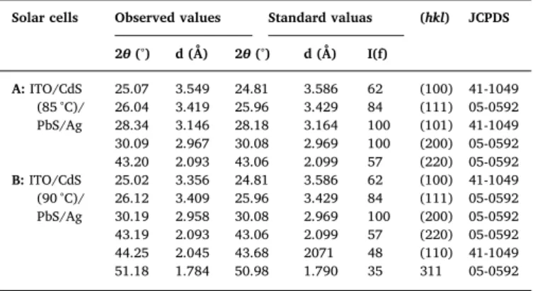
Moreover,Fig. 4shows the XRD spectra for thin film solar cells A and B. As can be seen from this figure, the solar cells exhibit mixing of hexagonal CdS and cubic PbS phases. Cubic phase of PbS is more dominant than hexagonal CdS phase. Substrate (ITO) effect is still seen but it is less effective in solar cell B. Structural properties of solar cells are given inTable 3.
3.2. Surface morphology
The surface morphology of the nanoparticles plays an important role in the behavior of solarcells. Therefore, the solar cell performance can be better investigated via understanding the image of these nano-particles. The SEM and AFM images of CdS and PbS films as well as solar cells were analyzed to make a better correlation between mor-pholgy and photovoltaic performance. Fig. 5shows the SEM micro-graphs of ITO substrate, CdS films, PbS films and solar cells.Fig. 5(a) shows micrograph of the substrate (ITO). It can be seen that the CdS film deposited at 85 °C shows worthy like structure, whose distributions on the surface are homogeneous and dense inFig. 5(b), while other CdS film deposited at 90 °C indicates spherical nanoparticles with different size and shapes. Among the nanoparticles, voids can be observed in Fig. 5(c). On the other hand, the PbS nanoparticles have randomly grown islands with different size and shapes, whose distributions on the surface are uniform [2]as seen in Fig. 5(d). It can be noticed that surface morphology of solar cell A inFig. 5(e) is similar to surface of the PbS film while surface morphology of solar cell B inFig. 5(g) looks like surface of CdS film (Fig. 5(c)).Figs. 5(f) and5(h) show cross sectional images of solar cells A and B, respectively. The CdS and PbS layer thicknessess measured from the cross sectional SEM image of solar cell A is found to be ~384 nm and ~223 nm, respectively, while for solar cell B, they are measured as ~375 nm and ~219 nm, respectively.
Additionally,Fig. 6shows two and three dimensional AFM images of present thin films and solar cells. It is seen that solar cell B in Fig. 6(h) exhibits a more smooth surface than the solar cell A in Fig. 6(j).
3.3. Optical properties
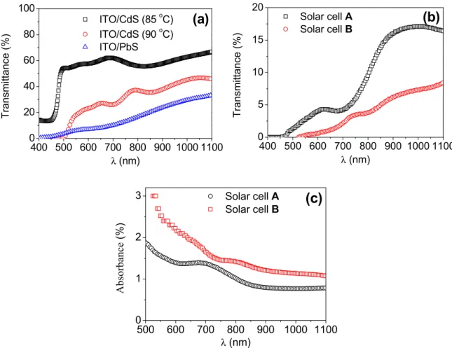
The optical transmittance (T) and absorbance (A) spectra of thin films and solar cells are given in Fig. 7. As seen in Fig. 7(a), the transmittance values of the CdS thin films produced at 85 °C and 90 °C are ~63% and ~37%, respectively. The PbS thin film has a very low transmittance. The transmittance of solar cell A is higher than the solar cell B as shown inFig. 7(b). Moreover, transmittance values of solar cells inFig. 7(b) are lower in comparison with individual transmission values of CdS and PbS thin films inFig. 7(a). The thickness and optical scattering mechanisms of the films and solar cells are very important parameters in understanding the optical properties. The increase in transmittance of the films and solar cells may be attributed to the less
Table 3
Structural properties of solar cells.
Solar cells Observed values Standard valuas (hkl) JCPDS 2θ (°) d (Å) 2θ (°) d (Å) I(f) A: ITO/CdS (85 °C)/ PbS/Ag 25.07 3.549 24.81 3.586 62 (100) 41-1049 26.04 3.419 25.96 3.429 84 (111) 05-0592 28.34 3.146 28.18 3.164 100 (101) 41-1049 30.09 2.967 30.08 2.969 100 (200) 05-0592 43.20 2.093 43.06 2.099 57 (220) 05-0592 B: ITO/CdS (90 °C)/ PbS/Ag 25.02 3.356 24.81 3.586 62 (100) 41-1049 26.12 3.409 25.96 3.429 84 (111) 05-0592 30.19 2.958 30.08 2.969 100 (200) 05-0592 43.19 2.093 43.06 2.099 57 (220) 05-0592 44.25 2.045 43.68 2071 48 (110) 41-1049 51.18 1.784 50.98 1.790 35 311 05-0592
light scattering due to the better crystal structure and surface proper-ties. The absorption value of solar cell B is higher than the solar cell A as seen inFig. 7(c). This means that the solar cell B absorbs more light from UV to IR regions compared with the solar cell A. The optical properties as well as crystal structure and surface properties of the present films are very important for solar cell performance.
The optical band gap of the thin films and solar cells is evaluated using Tauc's relation[21]:
=
h B h( Eg)n (4)
whereais the absorption coefficient which is given by the relation of =
a –1/dlnT,Bis a constant, Egis the optical band gap of the material,
h is the photon energy and n is a constant which is equal to ½ for direct transition. The Egvalues were determined from the intercept of the linear region part of ah( )2against the h graph on the h axis. For
thin films and solar cells, ah( )2versus h were plotted inFig. 8. The E
g
Fig. 5. SEM micrographs of (a) ITO substrate, (b) ITO/CdS (85 °C) thin film, (c) ITO/CdS (90 °C) thin film, (d) ITO/PbS thin film, (e) solar cell A, (f) cross sectional
values of thin films and solar cells were given inTable 4, which were in agreement with the values reported in the literature. Results inFig. 8(a) and (b) show that the Egvalues of CdS thin film deposited at 85 °C and 90 °C are 2.55 eV and 2.41 eV, respectively. The Eg value of PbS thin film was obtained as 1.39 eV inFig. 8(c).Fig. 8(d) andTable 4illustrate
Egvalues [A; (Eg1= 2.06 eV and Eg2= 1.55 eV) and B; (Eg1= 1.40 eV and Eg2= 1.19 eV)] of both CdS and PbS thin films. Moreover, optical parameters of the films and solar cells such as refractive index (n), extinction coefficient (k), real (1) and imaginary(2) parts of dielectric
constant were calculated from absorbance and transmittance spectra as seen inTable 4. These values are higher in solar cells compared with the individual values of CdS and PbS thin films and the highest in solar cell
B.
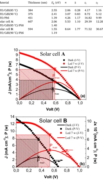
3.4. Solar cell parameters
The current density voltage (J-V) and power voltage curves of the solar cells A and B are given inFig. 9(a) and (b), respectively. From the J-V curves, short circuit current density (JSC), open voltage (VOC), fill factor (FF) and efficiency ( ) values were calculated using Eqs.(1) and (2)and listed inTable 5. After lightining at 7 W led lamp, it could be clearly seen that the value of solar cell A increases from 2.17% to 3.59%, while that of solar cell B increases from 2.75% to 4.85%. It could be concluded that synthesized solar cell B shows a better
Fig. 6. Two and three dimensional AFM images of (a,b) ITO/CdS (85 °C) thin film, (c,d) ITO/CdS (90 °C) thin film, (e,f) ITO/PbS thin film, (g,h) solar cell A, (i,j)
fotovoltaic performance than the solar cell A. This case may be attrib-uted to structure, morphology and optical properties of CdS layer which is used in the production of solar cell B. The highest efficiency is de-termined as 4.85% which is higher than those obtained for CdS/PbS solar cells in experimental works[2](1.63%),[1](3%),[22](4%) as well as theoretical work[3](4.13%). Nevertheless, it is lower than the
reported values (5.8% and 5.70%) by Manjceevan et al.[6,23]. Another important parameter is the FF. As seen inTable 5, after lightining, it increases from 0.30 to 0.38 for solar cell A and from 0.31 to 0.39 for solar cell B. An increment light-harvesting ability (higher ability of the absorption) and enhance charge transport ability of excited electron (the reduction of charge recombination) at the p-n junction [24–27] which can be verified by the UV–vis absorption spectra of solar cells seen inFig. 7(c) lead to a remarkable improvement in solar cell per-formance.
4. Conclusion
In order to obtain solar cell structures of ITO/CdS/PbS/Ag, window (CdS) and absorption (PbS) layers have been sequentially synthesized on ITO substrates using the CBD and SILAR methods, respectively. We have produced two solar cell in the structures of ITO/CdS/PbS/Ag using two different temperatures of 85 °C and 90 °C with two different am-monium hydroxide concentration of 1 M and 9.96 M, respectively for the CdS thin films. The structural, morphological and optical properties of CdS, PbS thin films and solar cells have been investigated. The XRD studies show that CdS films have polycrystalline hexagonal (wurtzite) structure while the PbS film has polycrystalline cubic structure. The SEM micrograph of CdS film surface deposited at 85 °C using 1 M am-monium hydroxide shows worth like morphology when the other CdS film deposited at 90 °C using 9.96 M ammonium hydroxide indicates spherical nanoparticle. The structural, morphological, optical and electrical properties of solar cells are influenced by an increment in ammonium hydroxide concentration in the CdS films. Hence, we have analyzed this effect on solar cell performance. The performance of solar cells has been characterized by current density-voltage measurements. After illumination with white led lamp, solar cell fabricated using CdS layer deposited at 90 °C with 9.96 M NH4OH shows higher efficiency
= 4.85% (JSC = 12.44 mA cm–2,VOC= 1 V, FF = 0.39) then the solar cell deposited using CdS layer deposited at 85 °C with 1 M NH4OH
in-dicates efficiency = 3.59% (JSC = 9.43 mA cm–2,VOC = 1 V, FF = 0.38). An improvement in solar cell performance can be attributed to an increment in light-harvesting ability and an enhancement in charge transport ability (reduction of charge recombination) at the p-n junc-tion. The results show that variation of ammonium hydroxide con-centration has impact on CdS process and modifies the growth of a film which leads to an improvement on thin film ITO/CdS/PbS solar cell performance.
Acknowledgement
The authors acknowledge financial support from Burdur Mehmet Akif Ersoy University, Burdur, Turkey (Project No. 0348-NAP-16). Conflict of interest
The authors declare that they have no conflict of interest.
Table 4
Thicknesses and optical properties of thin films and solar cells ( = 560 nm).
Material Thickness (nm) Eg(eV) n k 1 2
ITO/CdS(85 °C) 384 2.55 2.06 0.28 4.17 1.16 ITO/CdS(90 °C) 375 2.41 3.07 0.83 8.72 5.12 ITO/PbS 451 1.39 4.26 1.17 16.82 9.99 Solar cell A: 607 2.06 5.53 1.10 29.39 12.20 ITO/CdS(85 °C)/PbS 1.40 Solar cell B: 594 1.55 8.64 1.77 71.52 30.67 ITO/CdS(90 °C)/PbS 1.19
Fig. 9. Current density-voltage (J-V) and power-voltage (P-V) curves of
syn-thesized solar cells (a) A and (b) B.
Table 5
Solar cells parameters.
Solar cell Dark Lightening (Led 7 w lamp)
VOC(V) JSC(mA cm–2) FF (%) VOC(V) JSC(mA cm–2) FF (%)
A 1 7.212 0.30 2.17 1 9.432 0.38 3.59
References
[1] A. Kariper, E. Guneri, F. Gode, C. Gumus, T. Ozpozan, The structural, electrical and optical properties of CdS thin films as a function of pH, Mater. Chem. Phys. 129 (2011) 183–188.
[2] F. Gӧde, E. Güneri, F.M. Emen, V.E. Kafadar, S. Ünlü, Synthesis, structural, optical, electrical and thermoluminescence properties of chemically deposited PbS thin films, J. Lumin. 147 (2014) 41–48.
[3] E. Güneri, F. Göde, S. Çevik, Influence of grain size on structural and optic prop-erties of PbS thin films produced by SILAR method, Thin Solid Films 589 (2015) 578–583.
[4] C. Li, F. Wang, Y. Chen, L. Wu, J. Zhang, W. Li, X. He, B. Li, L. Feng, Characterization of sputtered CdSe thin films as the window layer for CdTe solar cells, Mater. Sci. Semicond. Process. 83 (2018) 89–95.
[5] M.-C. Chen, J.-C. Sung, C.-Y. Ou, S. Som, C.-H. Lu, Fast formation of CdS thin films prepared via the microwave-assisted chemical bath deposition process, Thin Solid Films 645 (2018) 64–69.
[6] M.P.A. Muthalif, Y.-S. Lee, C.D. Sunesh, H.-J. Kim, Y. Choe, Enhanced photovoltaic performance of quantum dot-sensitized solar cells with a progressive reduction of recombination using Cu-doped CdS quantum dots, Appl. Surf. Sci. 396 (2017) 582–589.
[7] J. Hernández-Borja, Y.V. Vorobiev, R. Ramírez-Bon, Thin film solar cells of CdS/PbS chemically deposited by an ammonia-free process, Sol. Energy Mater. Sol. Cells 95 (2011) 1882–1888.
[8] H.A. Mohamed, Theoretical study of the efficiency of CdS/PbS thin film solar cells, Sol. Energy 108 (2014) 360–369.
[9] M.A. Abbas, M.A. Basit, T.J. Park, J.H. Bang, Enhanced performance of PbS-sensi-tized solar cells via controlled successive ionic-layer adsorption and reaction, Phys. Chem. Chem. Phys. 17 (2015) 9752–9760.
[10] A. Manjceevan, J. Bandara, Systematic stacking of PbS/CdS/CdSe multi-layered quantum dots for the enhancement of solar cell efficiency by harvesting wide solar spectrum, Electrochim. Acta 271 (2018) 567–575.
[11] L. Jin, G. Sirigu, X. Tong, A. Camellini, A. Parisini, G. Nicotra, C. Spinella, H. Zhao, S. Sun, V. Morandi, M. Zavelani-Rossi, F. Rosei, A. Vomiero, Engineering interfacial structure in “Giant” PbS/CdS quantum dots for photoelectrochemical solar energy conversion, Nano Energy 30 (2016) 531–541.
[12] J. Li, Preparation and properties of CdS thin films deposited by chemical bath de-position, Ceram. Int. 41 (2015) S376–S380.
[13] S. Soundeswaran, O. Senthil Kumar, R. Dhanasekaran, Effect of ammonium sul-phate on chemical bath deposition of CdS thin films, Mater. Lett. 58 (2004)
2381–2385.
[14] N.S. Priya, S.S.P. Kamala, V. Anbarasu, S.A. Azhagan, R. Saravanakumar, Characterization of CdS thin films and nanoparticles by a simple chemical bath technique, Mater. Lett. 220 (2018) 161–164.
[15] P. Nair, J. Campos, M. Nair, Opto-electronic characteristics of chemically deposited cadmium sulphide thin films, Semicond. Sci. Technol. 3 (1988) 134.
[16] P. Roy, S.K. Srivastava, A new approach towards the growth of cadmium sulphide thin film by CBD method and its characterization, Mater. Chem. Phys. 95 (2006) 235–241.
[17] N. Mir, A.A. Mir, P. Karimi, N. Poormolaei, Effect of chelating reagents on nanos-tructured CdS layer morphology in CdS-sensitized TiO2 solar cells by successive ionic layer adsorption and reaction (SILAR) method, Mater. Sci. Semicond. Process. 77 (2018) 1–7.
[18] S.B. Patil, A.K. Singh, Effect of complexing agent on the photoelectrochemical properties of bath deposited CdS thin films, Appl. Surf. Sci. 256 (2010) 2884–2889. [19] D.G. Jensen, Alloys in Cadmium Telluride Solar Cells (Thesis), University of
Stanford, USA, 1997.
[20] F. Gӧde, C. Gümüş, M. Zor, Investigations on the physical properties of the poly-crystalline ZnS thin films deposited by the chemical bath deposition method, J. Cryst. Growth 299 (2007) 136–141.
[21] J.I. Pankove, Optical Processes in Semiconductors, Dover, New York, 1975. [22] V. Gonzalez-Pedro, C. Sima, G. Marzari, P.P. Boix, S. Gimenez, Q. Shen, T. Dittrich,
I. Mora-Sero, High performance PbS Quantum Dot Sensitized Solar Cells exceeding 4% efficiency: the role of metal precursors in the electron injection and charge separation, PCCP 15 (2013) 13835–13843.
[23] A. Manjceevan, J. Bandara, Robust surface passivation of trap sites in PbS q-dots by controlling the thickness of CdS layers in PbS/CdS quantum dot solar cells, Sol. Energy Mater. Sol. Cells 147 (2016) 157–163.
[24] X. Zhang, Y. Lin, J. Wu, J. Jing, B. Fang, Improved performance of CdSe/CdS/PbS co-sensitized solar cell with double-layered TiO2 films as photoanode, Opt. Commun. 395 (2017) 117–121.
[25] X. Zhang, Y. Lin, J. Wu, B. Fang, J. Zeng, Improved performance of CdSe/CdS co-sensitized solar cells adopting efficient CuS counter electrode modified by PbS film using SILAR method, Opt. Commun. 412 (2018) 186–190.
[26] Y.-D. Chung, D.-H. Cho, N.-M. Park, K.-S. Lee, J. Kim, Effect of annealing on CdS/Cu (In,Ga)Se2 thin-film solar cells, Curr. Appl. Phys. 11 (2011) S65–S67.
[27] Y. Chen, Q. Tao, W. Fu, H. Yang, Synthesis of PbS/Ni2+ doped CdS quantum dots cosensitized solar cells: enhanced power conversion efficiency and durability, Electrochim. Acta 173 (2015) 812–818.