ELECTRICALLY UNBIASED AND HALF
FREQUENCY DRIVEN WATERBORNE
16×16-ELEMENT 2-D PHASED ARRAY
CMUT
A THESIS SUBMITTED TO
THE GRADUATE SCHOOL OF ENGINEERING AND SCIENCE OF BILKENT UNIVERSITY
IN PARTIAL FULFILLMENT OF THE REQUIREMENTS FOR THE DEGREE OF
MASTER OF SCIENCE IN
ELECTRICAL AND ELECTRONICS ENGINEERING
By
Kerem Enhoş
ii
Electrically Unbiased and Half Frequency Driven Waterborne 16×16-Element 2-D Phased Array CMUT
By Kerem Enhoş August 2019
We certify that we have read this thesis and that in our opinion it is fully adequate, in scope and in quality, as a thesis for the degree of Master of Science.
Hayrettin Köymen (Advisor)
Yusuf Ziya İder
Itır Köymen
Approved for the Graduate School of Engineering and Science:
Ezhan Karaşan
iii
ABSTRACT
ELECTRICALLY UNBIASED AND HALF FREQUENCY
DRIVEN WATERBORNE 16x16-ELEMENT 2-D
PHASED ARRAY CMUT
Kerem Enhoş
M.S. in Electrical and Electronics Engineering Advisor: Hayrettin Köymen
August 2019
Capacitive micromachined ultrasonic transducers (CMUT) are typically used as arrays consisting of separate cells or interconnected sub arrays, and these cells have several operation modes. Design procedure and measurements have been previously presented for an airborne CMUT cell without a DC bias. In unbiased mode, the plate motion spans the entire gap without collapsing. The frequency of sinusoidal electrical input signal is half of the resulting acoustical output signal. A large plate swing can be obtained at low excitation voltages using the entire remaining gap. In this work, a design procedure of arrays with unbiased operation mode is derived. Designs are validated by means of simulations and measurements on fabricated CMUTs. The problems associated with beamforming are resolved. Use of this operation mode in an array configuration enables larger acoustical power output. A better transmitted signal waveform definition is obtained when pulse width modulation (PWM) is employed.
In the design process of CMUTs, large-signal equivalent circuit model is used. In order to have volumetric transmission, a 16×16 (256 elements) phased array configuration is chosen. A design procedure is presented considering the radiation pattern, Rayleigh distance and the parameters of the lumped-element model. This procedure is applied for designing two arrays, with resonance
iv
frequencies at 7.5 MHz and at 18.5 MHz. Harmonic balance and transient analyses are carried out with Gaussian enveloped tone burst, transient sinusoidal and PWM signals with different duty cycles. Outputs of these simulations are fed in beamforming toolboxes for further verification. Corresponding experimental measurements are conducted on an ultrasound measurement system.
The dimensions of the CMUT elements in the array are determined as 80 µm element radius, 15 µm plate thickness, and 171 nm effective gap height at 7.5 MHz, where the center-to-center inter-element pitch is set at 192 µm. The array is designed such that it has maximum Rayleigh distance of 45.3 mm, while having a maximum sidelobe level of −17.4 dB. According to these specifications, CMUT array is manufactured using wafer scale batch compatible production. Only two lithography masks, which require conventional photolithography steps, are used in production. The vibrating plate is constructed with anodic wafer bonding and the fabricated CMUT array chip is integrated to PCB with flip-chip bonding.
Measurements are conducted for this novel device by integrating the CMUT array chip manufactured with MEMS techniques and conventional macro scale manufactured PCB by using impedance analyser.
Keywords: Capacitive Micromachined Ultrasonic Transducers, CMUT, MEMS,
Array, Unbiased Operation, Half Frequency Driven, Mutual Radiation Impedance, Waterborne, Volumetric Transmission, Large Signal Equivalent Circuit Model
v
ÖZET
BESLEMESİZ VE YARI FREKANSTA SÜRÜLEN
SUALTI 16x16-ELEMANLI 2-B FAZLI DİZİN CMUT
Kerem Enhoş
Elektrik ve Elektronik Mühendisliği, Yüksek Lisans Tez Danışmanı: Hayrettin Köymen
Ağustos 2019
Kapasitif mikroişlenmiş ultrasonic çeviriciler (CMUT), genellikle ayrı elemanlar veya birbirine bağlı alt dizinler halinde, farklı çalışma modlarıyla kullanılmaktadır. Daha once doğru akım (DA) kullanılmayan, havada çalışan, CMUT elemanı için tasarım prosedürü ve ölçümleri sunulmuştur. DA olmayan çalışma modunda CMUT membrane çökme olmadan, alt taş ile arasındaki boşluğun tamamını salınım için kullanabilmektedir. Elde edilen akustik çıkıştaki sinyalin frekansı, elektriksel girişteki sinusoidal alternatif akım sinyalin iki katıdır. Düşük sürme voltajlarında büyük membrane salınımları elde edilebilmektedir. Bu çalışmada, DA kullanılmayan CMUT dizinlerinin tasarım prosedürleri sunulmuştur. Tasarımlar simülasyonlar ve üretilen CMUT dizinleri ile yapılan deneylerle doğrulanmıştır. Hüzmelemeye ilişkin problemler çözümlenmiştir. Bu operasyon modunun dizin olarak kullanılması çok daha yüksek akustik çıkış gücü elde edilmesine olanak sağlamaktadır. Darbe genişlik modülasyonu (PWM) sinyali elektriksel giriş olarak kullanılarak daha iyi sinyal iletimi sağlanması hedeflenmiştir.
CMUT’ların tasarım sürecinde büyük işaret modeli kullanılmıştır. Hacimsel iletim yapabilmek için 16×16 (256 eleman) fazlı dizin konfigürasyonu kullanılmıştır. Tasarım prosedürü, Rayleigh uzunluğu ve yığın eleman modeli parametreleri dikkate alınarak oluşturulmuştur. Bu prosedür rezonans frekansları 7.5 MHz ve 18.5 MHz olan iki farklı dizin için uygulanmıştır. Farklı görev döngüleriyle Gauss dağılımlı ton darbesi, sürekli sinusoidal ve PWM sinyalleri kullanılarak harmonik dengeleme ve zaman alanı simülasyonları yapılmıştır.
vi
Doğrulama amacıyla bu simülasyonların sonuçları hüzmeleme analizi yapabilen yazılımlara girdi olarak verilmiştir. Simülasyonlara karşılık gelecek şekilde deneysel ölçümler de ultrason ölçüm cihazı kullanılarak elde edilmiştir.
7.5 MHz için tasarlanan CMUT dizinindeki elemanların boyutları 80 µm yarıçap, 15 µm membran kalınlığı, 171 nm efektif açıklık yüksekliği ve 192 µm iki eleman merkezleri arası açıklık olarak belirlenmiştir. Dizin tasarımına gore 45.3 mm Rayleigh uzunluğu ve -17.4 dB yankulak seviyesi elde edilmiştir. Belirlenen bu özelliklere göre CMUT dizini gofret ölçeğinde yığın fabrikasyon uyumlu üretim tekniği benimsenerek üretilmiştir. Üretim sürecinde konvansiyonel litografi adımları için kullanılmak üzere sadece iki litografi maskesi kullanılmıştır. Salınım yapan membran anodic gofret yapıştırma tekniği ile üretilmiş, fabrike edilen CMUT dizinleri fiskeli yonga teknolojisi kullanılarak baskılı devre kartlarına yapıştırılmıştır.
MEMS teknikleriyle üretilen ve konvansiyonel makro ölçekle üretilen devre kartlarına entegre edilen bu yeni cihazın ölçümleri ultrason ölçüm cihazı kullanılarak tamamlanmıştır. Simülasyon sonuçlarını doğrulamak adına basınç ölçümleri alınmıştır.
Anahtar Kelimeler: Kapasitif Mikroişlenmiş Ultrasonik Çeviriciler, CMUT,
MEMS, Dizin, Doğrusal (DA) Yüklemesiz Operasyon, Yarı Frekansta Sürülen, Mutual Radyasyon Empedansı, Suda Çalışan, Hacimsel Iletim, Büyük Işaret Eşdeğer Devre Modeli.
vii
Acknowledgements
I would like to express my sincerest gratitude to my advisor Prof. Hayrettin Köymen for his incredible guidance through my and this thesis’ development. I would like to thank him for teaching me everything I know, for his endless support, patience and belief in me since I first began to work with him as a senior undergraduate. I feel deeply indebted for his invaluable help and encouragement during my graduate studies, which lead me to take a good turn in my life.
I would also like to thank Prof. Atalar and the members of my thesis monitoring committee, Prof. Ziya İder, and Asst. Prof. Itır Köymen for their beneficial comments, feedbacks and support through development of this work.
Especially I would like to praise Akif Sinan Taşdelen for his incredible patience, guidance, friendship and mentorship since my senior undergraduate years. He always helped me on any difficulty I faced in the last three years.
I would also like to thank my colleagues; Dr. Saadettin Güler, Dr. Mehmet Yılmaz, Giray İlhan, Yasin Kumru, Cem Bülbül, Doğu Kaan Özyiğit and my friends; Özgün Karslı, Melih Aydınat, Serkut Şimsek.and to all other friends and colleagues, and most importantly Radio Bilkent family who had helped me but whose names could not be mentioned. Completion of this work could not be possible without their help and support.
I would like to thank to my mother Tuba, my father Bora and my brother Kaan for their love and trust. They supported me on my every choice and effort. I am so grateful for having such a wonderful family and for their endless support, patience and belief in me.
Lastly, I feel deeply indebted to my beloved fiancée Esin. I cannot thank her enough, who calmed me in peace despite all my whining, came to my aid in my every difficulty I faced and always approached me with love. I hope all this effort and time bring us a happy, peaceful and a meaningful life, together.
viii
Contents
1
Introduction 12
Design of Arrays 52.1 Lumped Element Model And Large Signal Equivalent Circuit …. 5 2.2 Design Considerations ………9
2.3 Single Cell and Array Parameters ……….10
2.4 Design Procedure of Waterborne CMUT Arrays ……….16
3
Simulation Results 193.1 Simulation Specifications ……….19
3.2 Harmonic Balance Analysis ………..21
3.3 Impedance Simulations ………28
3.4 Sinusoidal Wave ………...31
3.5 Gaussian Enveloped Tone Burst Signal……… 41
3.6 Pulse Width Modulation (PWM) ………..48
3.7 Radiation Pattern Simulations………... 60
3.8 Beamforming Simulations ………66
3.9 Pressure Field Pattern……… 72
3.10 Power and Intensity ………77
4
Fabrication 83ix
4.2 MEMS Process Flow ………85
4.2.1 Cavity ……….85
4.2.2 Bottom Electrode ………...91
4.2.3 Wafer Bonding & Top Electrode ………97
4.2.4 Flip-Chip Bonding & Sealing ………..104
4.2.5 CMUT-MEMS Fabrication Overview………. .108
5
Measurements 1105.1 Impedance Measurements………... 110
6
Conclusion 114A MATLAB Scripts 124
B Extra Graphics 130
B.1 Extra Simulation Graphics ………..130
B.2 Extra Fabrication Graphics ……….154
x
List of Figures
2.1 Cross-sectional view of circular CMUT and its clamped membrane deflection structure [29]. ... 5 2.2 Large signal equivalent circuit model for single CMUT cell. ... 6 2.3 Equivalent circuit model representation of the CMUT array with N cells, where the blocks denoted as ‘Cell’ consists of the large signal equivalent circuit shown in Figure 2.2. Fb is the static external force, such as that due to atmospheric pressure. fI is the dynamic external force, such as that due to an incident acoustic signal [29]. ... 8 2.4 Radiation pattern results of transmitter design for 7.5 MHz operation frequency. All figures are given as dB re. 1 µPa. a) Radiation pattern of a single cell with a = 80 µm, φ = 0 b) 3-D radiation pattern of a single cell for both elevation and azimuth plane, c) radiation pattern of 16x16 array with a = 80 µm and d = 192 µm, φ = 0 d) 3-D radiation pattern of the array. ... 12 2.5 Radiation pattern results of transmitter design for 18.5 MHz operation frequency. All figures are given as dB re. 1 µPa. a) Radiation pattern of a single cell with a = 32.2 µm, φ = 0 b) 3-D radiation pattern of a single cell for both elevation and azimuth plane, c) radiation pattern of 16x16 array with a = 32.2 µm and d = 77.8 µm, φ = 0 d) 3-D radiation pattern of the array. ... 13 3.1 Orientation and placement of the elements that will be analysed through this work. ... 20 3.2 Simulation flow diagram ... 21 3.3 Second harmonic results of harmonic balance analysis driven with 75 volts AC voltage and zero DC bias for 7.5 MHz transducer. ... 22
xi
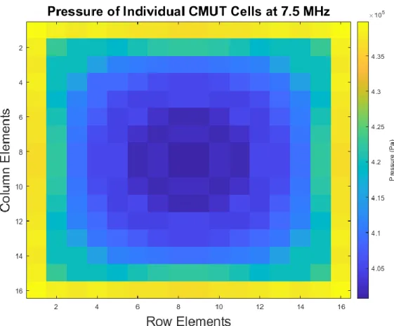
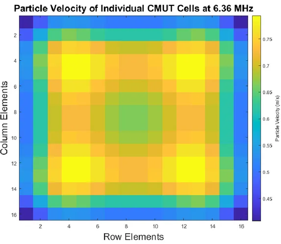
3.4 Heat map of pressure output of individual CMUT cells of the 16×16 phased array at the operation frequency, 7.5 MHz. ... 23 3.5 Heat map of pressure output of individual CMUT cells of the 16×16 phased array at the peak frequency, 6.36 MHz. ... 24 3.6 Particle velocity frequency domain analysis with 75 Vac input voltage. .... 25 3.7 Heat map of particle velocity output of individual CMUT cells of the 16×16 phased array at the operation frequency, 7.5 MHz. ... 25 3.8 Heat map of particle velocity output of individual CMUT cells of the 16×16 phased array at the peak frequency, 6.36 MHz. ... 26 3.9 Comparison between unbiased and biased mode of operation for corner (a), middle (b) and side (c) elements of the array. ... 27 3.10 Comparison of even harmonics of unbiased mode and all harmonics of the biased mode of operation for critical array elements. ... 27 3.11 Admittance at 75 Vac input voltage. Susceptance values are shown in dashed lines. ... 29 3.12 Admittance at 5 Vac input voltage. Susceptance values are shown in dashed lines. ... 30 3.13 Admittance values at 7.5 MHz for different AC input voltage levels. ... 30 3.14 Transient sinusoidal transient analysis with 5 volt input voltage at 3.75 MHz frequency is obtained. Acoustical output pressures resulted at 7.5 MHz. ... 32 3.15 Transient sinusoidal transient analysis with 75 volt input voltage at 3.75 MHz frequency is obtained. Acoustical output pressures resulted at 7.5 MHz. ... 32
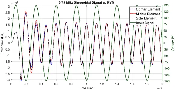
xii
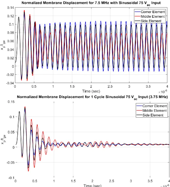
3.16 Normalized membrane displacement for 75 Vac (a) transient and (b) one cycle sinusoidal input signal is obtained as 0.1072 and 0.1333 respectively. ... 34 3.17 MVM voltage is found to be 149.2 Vac with 1.673 MPa peak pressure acoustical output at steady state. ... 35 3.18 Normalized membrane displacement for MVM at 149.2 volts. ... 36 3.19 Particle velocity is observed at 3.75 MHz input frequency and input voltage levels of 149.2 Vac (MVM) with one cycle sinusoidal waveforms. Two cycle of 7.5 MHz sine wave with 1.231 m/s peak velocity is obtained at acoustical output. ... 36 3.20 Transient analysis at peak frequency of 3.18 MHz electrical input and 6.36 MHz acoustical output. 75 volts of (a) Transient sinusoidal input resulted in 927.5 kPa peak pressure and (b) 1 cycle sinusoidal input is resulted in 492 kPa peak pressure. ... 37 3.21 Peak normalized membrane displacement at steady state is obtained as 0.2728 at peak frequency with 75 Vac. ... 38 3.22 Particle velocity is observed at peak frequency of 3.18 MHz input frequency and input voltage levels of 75 Vac with one cycle sinusoidal waveforms. At acoustical output 0.3065 m/s peak velocity is obtained. ... 38 3.23 Transient analysis at 3.75 MHz input frequency and input voltage level of 75 volts with half cycle sinusoidal waveforms. One cycle of 7.5 MHz sine wave with 299 kPa peak pressure is obtained at acoustical output. ... 39 3.24 Transient analysis at 3.75 MHz input frequency and input voltage levels of 75 volts with one cycle sinusoidal waveforms. Two cycle of 7.5 MHz sine wave with 459.9 kPa peak pressure is obtained at acoustical output. ... 40
xiii
3.25 Transient analysis at 3.75 MHz input frequency and input voltage levels of 75 volts with four cycle sinusoidal waveforms. Eight cycles of 7.5 MHz sine wave with 560.7 kPa peak pressure is obtained at acoustical output. . 40 3.26 Particle velocity is observed at 3.75 MHz input frequency and input voltage levels of 75 volts with one cycle sinusoidal waveforms. Two cycle of 7.5 MHz sine wave with 0.2732 m/s peak velocity is obtained at acoustical output. ... 41 3.27 Transient analysis at 3.75 MHz input frequency and input voltage level of 5 volts with 5 cycle Gaussian enveloped tone burst signal. 10 cycle of 7.5 MHz Gaussian enveloped tone burst signal with 2.256 kPa peak pressure is obtained at acoustical output. ... 42 3.28 Transient analysis at 3.75 MHz input frequency and input voltage level of 75 volts with 5 cycle Gaussian enveloped tone burst signal. 10 cycle of 7.5 MHz Gaussian enveloped tone burst signal with 498.1 kPa peak pressure is obtained at acoustical output. ... 42 3.29 Normalized membrane displacement for 75 Vac 5 cycle of Gaussian enveloped tone burst input signal at operation frequency of 3.75 MHz. ... 43 3.30 Maximum peak particle velocity for 75 Vac 5 cycle of Gaussian enveloped tone burst input signal at operation frequency of 3.75 MHz is found to be 0.2272 m/s. ... 44 3.31 (a) Peak pressure of 2.764 MPa of acoustical output is obtained at MVM with 186.15 Vac. (b) Normalized membrane displacement is calculated for MVM. ... 45 3.32 Maximum peak particle velocity for 186.15 Vac (MVM) 5 cycle of Gaussian enveloped tone burst input signal is found to be 1.362 m/s. ... 46
xiv
3.33 5 cycle Gaussian enveloped tone burst signal is driven at peak frequency of 3.18 MHz with 75 Vac. (a) 807.4 kPa peak pressure is obtained at acoustical output with ten cycle Gaussian enveloped tone burst signal at 6.36 MHz. (b) Maximum peak particle velocity for 75 Vac 5 cycle of Gaussian enveloped tone burst input signal at peak frequency of 3.18 MHz is found to be 0.5268 m/s. ... 47 3.34 Maximum peak normalized membrane displacement is found to be 0.2415 for peak frequency input of 5 cycle Gaussian enveloped tone burst signal. ... 48 3.35 Transient PWM signal is given as input at 3.75 MH with 75 Vac. Sinusoidal waveform is resulted at acoustical output with 7.5 MHz and 456.5 kPa peak pressure at steady state. ... 50 3.36 Transient analysis at 3.75 MHz input frequency and input voltage levels of 75 volts with half cycle PWM signal. One cycle of 7.5 MHz sinusoidal wave with 383.2 kPa peak pressure is obtained at acoustical output. ... 51 3.37 Transient analysis at 3.75 MHz input frequency and input voltage levels of 75 volts with one cycle PWM signal. Two cycle of 7.5 MHz sinusoidal wave with 598.9 kPa peak pressure is obtained at acoustical output. ... 51 3.38 Transient analysis at 3.75 MHz input frequency and input voltage levels of 75 volts with four cycle PWM signal. Eight cycle of 7.5 MHz sinusoidal wave with 651.9 kPa peak pressure is obtained at acoustical output. ... 52 3.39 Normalized membrane displacement for (a) transient and (b) 1 cycle of PWM signal input. Peak normalized membrane displacement for both transmissions are simulated to be 0.1697. ... 53 3.40 Maximum peak particle velocity for 75 Vac 1 cycle PWM input signal at operation frequency of 3.75 MHz is found to be 0.3175 m/s. ... 54
xv
3.41 Transducer is driven at MVM with 131 Vac. With (a) transient PWM input 1.383 MPa peak pressure is obtained at steady state. For (b) 1 cycle transmission of PWM signal, 2.381 MPa of peak pressure is obtained. .... 55 3.42 Normalized membrane displacement for (a) transient and (b) one cycle PWM input at 3.75 MHz with MVM. ... 56 3.43 Maximum peak particle velocity for 131 Vac (MVM) 1 cycle PWM input signal at operation frequency of 3.75 MHz is found to be 1.31 m/s. ... 57 3.44 Transducer is driven at peak frequency of 3.18 MHz with 75 Vac. With (a) transient PWM input 1.178 MPa peak pressure is obtained at steady state. For (b) 1 cycle transmission of PWM signal, 613.1 kPa of peak pressure is obtained. ... 58 3.45 With (a) transient PWM input 0.6626 m/s peak particle velocity is obtained at steady state. For (b) 1 cycle transmission of PWM signal, 0.3352 m/s of peak particle velocity is obtained. ... 59 3.46 With (a) transient PWM input, peak normalized membrane displacement is obtained as 0.3034 at steady state. For (b) 1 cycle transmission of PWM signal, peak normalized membrane displacement is obtained as 0.1918. .. 60 3.47 Orientation and placement of CMUT array in k-wave simulation space. .. 62 3.48 Simulation space constructed in k-wave with 32 µm grid (voxel) size and transmission medium dimensions of 15.744×32.128×3.456 mm. Transducer is placed at x=0 and the sensors are placed radially with a radius of 15.744 mm. ... 64 3.49 Radiation pattern simulation result obtained by k-wave and computational radiation pattern is shown. ... 66 3.50 N point source demonstration for (3.5) [37]. ... 67
xvi
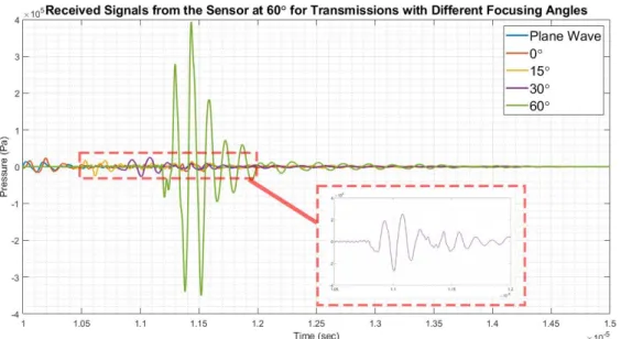
3.51 Input delays calculated by MATLAB is compared with the lag values obtained by the cross-correlation results of two consecutive CMUT elements’ time domain pressure outputs driven with 1 cycle PWM signal in ADS in a row of the phased array. ... 68 3.52 Plane wave transmission compared to beamformed transmission with different focusing angles. R-plane is shown in dB re. 1 µPa. ... 69 3.53 Received signals from the sensor at 0˚ (41st
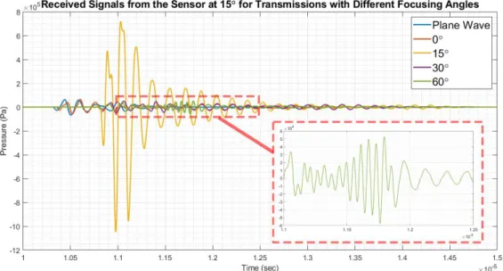
sensor) located on the k-wave simulation space, for different transmissions. Side lobe level is calculated to be 25.93 dB and RayleighBloch wave peak pressure difference to be -33.39 dB. ... 70 3.54 Received signals from the sensor at 15˚ (47th
sensor) located on the k-wave simulation space, for different transmissions. Side lobe level is calculated to be 25.28 dB and RayleighBloch wave peak pressure difference to be -33.67 dB. ... 70 3.55 Received signals from the sensor at 30˚ (53rd
sensor) located on the k-wave simulation space, for different transmissions. Side lobe level is calculated to be 23.85 dB and RayleighBloch wave peak pressure difference to be -33.83 dB. ... 71 3.56 Received signals from the sensor at 0˚ (59th
sensor) located on the k-wave simulation space, for different transmissions. Side lobe level is calculated to be 23.33 dB and RayleighBloch wave peak pressure difference to be -32.21 dB. ... 71 3.57 Field pattern resulted by plane wave transmission (zero delay) in k-wave at 7.5 MHz. ... 73 3.58 Field pattern resulted by 0˚ focused transmission in k-wave at 7.5 MHz and 15.744 mm distance to the center of the transducer surface. ... 73
xvii
3.59 Field pattern resulted by 0˚ focused transmission in k-wave at 7.5 MHz and 7.872 mm distance to the center of the transducer surface... 74 3.60 Field pattern resulted by 0˚ focused transmission in k-wave at peak frequency, 6.36 MHz and 7.872 mm distance to the center of the transducer surface. ... 75 3.61 Field pattern resulted by 30˚ focused transmission in k-wave at 7.5 MHz and 15.744 mm distance to the center of the transducer surface. ... 75 3.62 Field pattern resulted by 0˚ focused transmission in k-wave at 7.5 MHz and 7.872 mm distance to the center of the transducer surface with biased mode of operation. ... 76 3.63 Second harmonic of the harmonic balance analysis is shown for mechanical power for individual CMUT cells. Radiated power at 7.5 MHz is found for corner, middle and side CMUT elements as 0.997×10⁻³, 0.777×10⁻⁶, and 0.557×10⁻³ Watt respectively. ... 78 3.64 Second harmonic of the harmonic balance analysis is shown for mechanical power for the transducer by superimposing every CMUT element in the transducer array. Total radiated power for the transducer is found to be 86.6 mW. ... 78 3.65 Heat map of radiated power from individual CMUT cells of the 16×16 phased array at the operation frequency of 7.5 MHz. ... 79 3.66 Heat map of radiated power from individual CMUT cells of the 16×16 phased array at the peak frequency of 6.36 MHz. ... 80 3.67 Every harmonic data resulted from harmonic balance analysis for radiated power is shown. Odd harmonics of the fundamental of the electrical drive frequency is at a level of 10-30, which can be interpreted as numerical error; hence it is equal to zero. For even harmonics, radiated power decays
xviii
linearly with a rate of 10-3 until 18th harmonic and then stays at same level. ... 81 4.1 Full device mask design of 7.5 MHz (left) and the 16x16 CMUT array mask design (right). ... 84 4.2 180-element mask design for 18.5 MHz resonance frequency array. ... 85 4.3 Microscope image after lithography process is done. ... 86 4.4 Stylus profilometer measurement conducted after eleven cycles of ICP with argon plasma for etching chrome hard mask from the bottom electrode regions. The value shown in the figure is the depth of the etched pyrex with adding the chrome thickness of the hard mask. ... 87 4.5 Microscope image after hard baking of the photoresist for 1.5 hours with 110˚C and 3 hours with 150˚C. Distortion of the shape on the photoresist can be seen. ... 89 4.6 On the left side ESEM image after the dry etch process is shown. Undercuts are resulted after DRIE. The thin layer of metal is the chrome mask deposited at the beginning of the processes. On the right image, stylus profilometer result for the depth of the etched Pyrex cavity is shown for 90 minutes of DRIE with SF6 and argon plasma. The chrome thickness is also included in the measurement for greater comparison with the results obtained after ICP chrome etching. ... 89 4.7 (a) ESEM image after applying 6 minutes of BOE. Cross-sectional view of the 3 µm wires can be seen. Residues are due to the cracking of the wafer. (b) Microscope image after wet etching with BOE. (c) Sytlus profilometer measurement showing that the depth of the cavity is increased from 851 nm (Figure 7) to 978 nm by applying 6 minutes of BOE (≈127 nm of etching, which is consistent with the calculated etch rate). The chrome thickness is
xix
also included in these measurements for easier comparison with previous results and data. ... 90 4.8 Microscope images after depositing 100 nm Ti, 100nm Pt and 500 nm Au (before lift-off). ... 91 4.9 Focused ion beam (FIB) image of the cross-section of the Ti/Pt/Au stack deposited on silicon sample. ... 92 4.10 (a) Before and (b) after etching the insulator layer, Alumina. ... 94 4.11 (a) Wafer 1 and (b) Wafer 2 substrate before wafer bonding... 96 4.12 Stylus profilometer measurements from (a) wafer 1 – 11th device and (b) wafer 2 – 15th device, which results in 216.7 nm and 118.5 nm gap heights respectively. ... 97 4.13 Bonded and unbonded areas are shown for wafer 2 for the first (a) and second (b) bonding process with increased temperature and voltage. ... 99 4.14 Wafer 1 after wafer bonding with the modified recipe of 1000 volts and 450˚C. ... 99 4.15 Defects on metals of electrical connection pads after wafer bonding process. ... 100 4.16 Wafer 2 (a) and wafer 1 (b) after 350 µm thick handle layer removal with SF6 plasma DRIE. ... 100 4.17 Wafer 1 after metal deposition with shadow mask. ... 101 4.18 Wafer 1 after silicon dry etch with DRIE Bosch process. ... 102 4.19 Wafer 1 after photoresist stripping and chrome etch with O2 plasma dry etch. ... 103
xx
4.20 Finalized MEMS chip of 16×16 CMUT phased array. ... 104 4.21 Wire bonding of ground connection pads and flip-chip bonded device. .. 105 4.22 Front side (a) (transmission side) and the backside of the bonded MEMS chip and PCB. ... 106 4.23 Probe integration. ... 107 4.24 Fabrication flow of CMUT arrays manufactured at Bilkent University. . 109 5.1 Admittance of 8th element of the 7th device. Resonance is measured at 6.94 MHz with 19.24 µS in air. ... 111 5.2 Admittance of 58th element of the 7th device. Resonance is measured at 6.45 MHz with 38.65 µS in air. ... 111 5.3 Conductance of 156th element of the 7th device. Change in resonance frequency and conductance level for different DC bias can be seen. At zero DC bias the resonances can be observed. ... 112 B.1 Admittance at 15 Vac input voltage. Susceptance values are shown in dashed lines. ... 130 B.2 Admittance at 35 Vac input voltage. Susceptance values are shown in dashed lines. ... 131 B.3 Admittance at 55 Vac input voltage. Susceptance values are shown in dashed lines. ... 131 B.4 Normalized membrane displacement for 5 volt transient sinusoidal input signal at 3.75 MHz. ... 132 B.5 Transient analysis at 3.75 MHz input frequency and input voltage level of 5 volts with half cycle sinusoidal waveforms... 132
xxi
B.6 Transient analysis at 3.75 MHz input frequency and input voltage level of 5 volts with one cycle sinusoidal waveforms. ... 133 B.7 Transient analysis at 3.75 MHz input frequency and input voltage level of 5 volts with four cycle sinusoidal waveforms. ... 133 B.8 Normalized membrane displacement for 5 volt half cycle sinusoidal input signal at 3.75 MHz. ... 134 B.9 Normalized membrane displacement for 5 volt 1 cycle sinusoidal input signal at 3.75 MHz. ... 134 B.10 Normalized membrane displacement for 5 volt 4 cycle sinusoidal input signal at 3.75 MHz. ... 135 B.11 Normalized membrane displacement for 75 volt half cycle sinusoidal input signal at 3.75 MHz. ... 135 B.12 Normalized membrane displacement for 75 volt 4 cycle sinusoidal input signal at 3.75 MHz. ... 136 B.13 Transient analysis at 3.75 MHz input frequency and input voltage level of 149.2 Vac (MVM) with half cycle sinusoidal waveforms. ... 136 B.14 Transient analysis at 3.75 MHz input frequency and input voltage level of 149.2 Vac (MVM) with 1 cycle sinusoidal waveforms. ... 137 B.15 Transient analysis at 3.75 MHz input frequency and input voltage level of 149.2 Vac (MVM) with 4 cycle sinusoidal waveforms. ... 137 B.16 Transient analysis at peak frequency of 3.18 MHz and input voltage level of 75 Vac with 4 cycle sinusoidal waveforms. ... 138 B.17 Particle velocity obtained for half cycle sinusoidal input with operation frequency 3.75 MHz and 75 Vac. ... 138
xxii
B.18 Particle velocity obtained for 4 cycle sinusoidal input with operation frequency 3.75 MHz and 75 Vac. ... 139 B.19 Particle velocity obtained for half cycle sinusoidal input with operation frequency 3.75 MHz and 149.2 Vac (MVM). ... 139 B.20 Particle velocity obtained for 4 cycle sinusoidal input with operation frequency 3.75 MHz and 149.2 Vac (MVM). ... 140 B.21 Particle velocity obtained for half cycle sinusoidal input with peak frequency 3.18 MHz and 75 Vac. ... 140 B.22 Particle velocity obtained for 4 cycle sinusoidal input with peak frequency 3.18 MHz and 75 Vac. ... 141 B.23 Normalized membrane displacement for 5 cycle Gaussian enveloped tone burst signal at operation frequency of 3.75 MHz and 5 Vac. ... 141 B.24 Transient analysis at operation frequency of 3.75 MHz and input voltage level of 5 Vac with transient PWM waveforms. ... 142 B.25 Transient analysis at operation frequency of 3.75 MHz and input voltage level of 5 Vac with half cycle PWM waveforms. ... 142 B.26 Transient analysis at operation frequency of 3.75 MHz and input voltage level of 5 Vac with 1 cycle PWM waveforms. ... 143 B.27 Transient analysis at operation frequency of 3.75 MHz and input voltage level of 5 Vac with 4 cycle PWM waveforms. ... 143 B.28 Normalized membrane displacement for operation frequency of 3.75 MHz and input voltage level of 5 Vac with transient PWM waveforms. ... 144 B.29 Normalized membrane displacement for operation frequency of 3.75 MHz and input voltage level of 5 Vac with half cycle PWM waveforms. ... 144
xxiii
B.30 Normalized membrane displacement for operation frequency of 3.75 MHz and input voltage level of 5 Vac with 1 cycle PWM waveforms. ... 145 B.31 Normalized membrane displacement for operation frequency of 3.75 MHz and input voltage level of 5 Vac with 4 cycle PWM waveforms. ... 145 B.32 Normalized membrane displacement for operation frequency of 3.75 MHz and input voltage level of 75 Vac with half cycle PWM waveforms. ... 146 B.33 Normalized membrane displacement for operation frequency of 3.75 MHz and input voltage level of 75 Vac with 4 cycle PWM waveforms. ... 146 B.34 Transient analysis at operation frequency of 3.75 MHz and input voltage level of 131 Vac (MVM) with half cycle PWM waveforms. ... 147 B.35 Transient analysis at operation frequency of 3.75 MHz and input voltage level of 131 Vac (MVM) with 4 cycle PWM waveforms. ... 147 B.36 Normalized membrane displacement for operation frequency of 3.75 MHz and input voltage level of 131 Vac (MVM) with half cycle PWM waveforms. ... 148 B.37 Transient analysis at peak frequency of 3.18 MHz and input voltage level of 75 Vac with half cycle PWM waveforms. ... 148 B.38 Transient analysis at peak frequency of 3.18 MHz and input voltage level of 75 Vac with 4 cycle PWM waveforms. ... 149 B.39 Normalized membrane displacement at peak frequency of 3.18 MHz and input voltage level of 75 Vac with half cycle PWM waveforms. ... 149 B.40 Normalized membrane displacement at peak frequency of 3.18 MHz and input voltage level of 75 Vac with 4 cycle PWM waveforms. ... 150 B.41 Particle velocity observed at operation frequency of 3.75 MHz and input voltage level of 75 Vac with half cycle PWM waveforms. ... 150
xxiv
B.42 Particle velocity observed at operation frequency of 3.75 MHz and input voltage level of 75 Vac with 4 cycle PWM waveforms. ... 151 B.43 Particle velocity observed at operation frequency of 3.75 MHz and input voltage level of 131 Vac (MVM) with half cycle PWM waveforms. ... 151 B.44 Particle velocity observed at operation frequency of 3.75 MHz and input voltage level of 131 Vac (MVM) with 4 cycle PWM waveforms. ... 152 B.45 Particle velocity observed at peak frequency of 3.18 MHz and input voltage level of 75 Vac with half cycle PWM waveforms. ... 152 B.46 Particle velocity observed at peak frequency of 3.18 MHz and input voltage level of 75 Vac with 4 cycle PWM waveforms. ... 153 B.47 Designed 0.4 mm PCB for flip-chip bonding and CMUT cell connection.
... 154 B.48 Reference numbers and placement orientation for each device on Pyrex wafer. ... 154 B.49 Admittance of 41st element of the 7th device. ... 156 B.50 Admittance of 72nd element of the 7th device. ... 156 B.51 Admittance of 79th element of the 7th device. ... 157 B.52 Admittance of 92nd element of the 7th device. ... 157 B.53 Admittance of 142nd element of the 7th device. ... 158 B.54 Admittance of 175th element of the 7th device. ... 158 B.55 Conductance of 156th element of the 7th device with different bias voltages. At -10 VDC resonances are disappearing and at 0 V resonances can be observed, which indicates the charging of the fabricated devices... 159
xxv
List of Tables
2.1 Parameters of the lumped elements of the large signal equivalent circuit model for single CMUT cell shown in Figure 2.2... 7 2.2 Membrane (Silicon) and insulator (Alumina) parameters that is taken for calculation and simulation in this work. ... 14 2.3 Designed CMUT parameters for two different operation frequencies. ... 18 3.1 Total harmonic distortion comparison for different CMUT elements in the array for unbiased and biased mode of operation. ... 28 3.2 dr(3 dB) in terms of wavelength is shown for different drive frequencies, focus angles and depths. λ is the wavelength of the operation frequency of 7.5 MHz and λP is the wavelength of the peak frequency, 6.36 MHz. ... 77 3.3 Power and intensity values obtained for different transmission schemes and different cycles over the transducer surface. ... 82 B.1 Two different stylus profilometer measurements (M1 & M2) from two different locations of the same device are taken for each device on both wafers. Averages of these two measurements (AV) are also included. ... 155
1
Chapter 1
Introduction
Capacitive micromachined ultrasonic transducers (CMUTs) are first introduced as surface micromachined electrostatic ultrasonic air transducers in 1994 [1] [2]. Rapidly after definition of CMUTs, usage of these devices considered in waterborne and similarly biomedical applications [3] [4]. Wide bandwidth nature [5], different operation modes, such as collapsed, [6] [7] uncollapsed and [8] unbiased (or charged) [9] [10], and compatibility of these devices lead them to be more popular with increased research.
CMUTs are devices that consists a substrate and a moving membrane with a gap designated between these two elements. Substrate and the membrane are used as electrodes for electroacoustic transduction. Using this substrate also as a membrane is presented earlier as bilateral CMUT cells [11]. CMUTs are widely used for receivers because of their high signal-to-noise ratio, which is limited by the noise of the integrated electronics. Also transmitting CMUTs are highly researched to compete with the high power transmission with conventional piezoelectric transducers [12]. Even though sufficient power or received signal can be maintained by using single CMUT cells, for beamforming and higher power transmission capabilities, CMUT arrays are widely used [13] [14].
Another attractive feature of CMUTs is the applicability of micromachining techniques on the fabrication of these devices [15]. Number of different fabrication methods are applied and presented for these devices. Two main methods are discussed, which are wafer bonding [16] and sacrificial layer release processes [17]. Within the sacrificial release processes, commercial multi-user compatible processes are also utilized, such as PolyMUMPS [18]. For wafer bonding process, bonding of a dielectric such as Pyrex as the substrate and a conducting membrane for top electrode such as silicon wafer can be used with a dielectric layer between top and bottom electrode. Conventional MEMS
2
processes can be applied for bottom electrode fabrication, dielectric layer deposition and gap formation. With the use of wafer bonding, batch compatible wafer scale microfabrication is utilized, which is a huge advantage for mass production of these devices. By this way large number of devices can be manufactured on a single wafer for commercial use. Along with the advantages of MEMS processes, also integration of electronics with these devices becomes an attractive issue. For this purpose flip-chip bonding [19] or CMUT-on-CMOS arrays [20] are widely used.
Though, CMUT devices are impressive with its fabrication and operational advantages, design and modelling of these devices is a cumbersome process. Commercial finite element modelling (FEM) tools are widely used for designing and simulating these devices [21] and huge improvements are gathered with the development of computational power [22]. For mechanical characterization and understanding the principles of these devices FEM is seen as a suitable tool [23]. However, using FEM for arrays with large number of CMUT cells is not a feasible option. Thus, several lumped-element models are presented for modelling both receiver (small signal) and transmitter (large signal) structures of these devices for different mode of operations [24] [8] [10]. By considering the mutual radiation impedance, simulations of arrays with large number of elements also become applicable [25]. With the use of equivalent circuit models, conventional lumped-element circuit model simulators can be used, which significantly decreases the computational time. Thus, using a conventional circuit simulator that can solve nonlinear operations creates a simple and practical simulation environment. Another advantage of using lumped-element modelling in CMUTs is that the formation and analysis of spurious resonances, such as Rayleigh-Bloch wave resonances on the surface of the transducer [26]. Similar spurious resonances and non-uniformities is observed and analysed with this method [27], where in FEM it is not possible.
In this work; modelling, simulation, fabrication and experimental verification of transmitting waterborne CMUT array with 256 elements (16×16
3
array configuration) by using the unbiased mode of operation is done. Design procedure and measurements were presented for an airborne CMUT cell without a DC bias earlier [9]. Several advantages come along with the unbiased mode of operation. In unbiased mode, the frequency of sinusoidal electrical input signal is half of the resulting acoustical output signal and the plate motion spans the entire gap without collapsing. A large plate swing can be obtained at low excitation voltages using the entire remaining gap. Using the entire gap for plate swing with DC bias is not possible due to the collapsing feature determined by the CMUT biasing chart [28]. Thus, using the entire gap for plate motion or swing gathers a huge advantage for transmitting CMUTs, which results in higher acoustical power output for lower excitation voltages.
In this work, a design procedure of arrays with unbiased operation mode is derived. Designs are validated by means of simulations and measurements on fabricated CMUTs. The problems associated with beamforming are resolved. Use of this operation mode in an array configuration enables larger acoustical power output. A better transmitted signal waveform definition is obtained when pulse width modulation (PWM) is employed.
In the design process of CMUTs, large-signal equivalent circuit model is used. In order to have volumetric transmission, a 16×16 (256 elements) phased array configuration is chosen. Considering the radiation pattern, Rayleigh distance and the parameters of the lumped-element model, a design procedure is presented. This procedure is applied for designing two arrays, with resonance frequencies at 7.5 MHz and at 18.5 MHz.
Harmonic balance simulations are conducted for frequency spectrum of pressure output, impedance analyses and power computations of the array. Also transient analyses are carried out with gaussian enveloped tone burst, transient sinusoidal and PWM signals with different duty cycles. Mainly pressure outputs and particle velocities of the cells are investigated. As an addition for each transmission waveform Rayleigh-Bloch waves are observed and minimum voltage mode (MVM) is investigated where MVM is the minimum voltage that
4
the membrane of the CMUT cells can maintain swing over the entire gap height. According to these time domain simulations, power and intensity results are also obtained. Finally, outputs of these simulations are fed in beamforming toolboxes such as k-wave in MATLAB for further verification. Radiation pattern and applicability of conventional beamforming techniques on these transducers are discussed. These results are also used for obtaining field patterns for different transmission schemes.
Designed devices are fabricated by using conventional MEMS processes and wafer bonding technique with using Pyrex wafer as the substrate and silicon wafer as the membrane. Gap heights, insulation and electrode layer thicknesses are applied on Pyrex wafer within a batch compatible wafer scale microfabrication process. Self-aligned process is used where all of the features fabricated on the substrate, Pyrex, are manufactured by using a single conventional photo lithography mask. In total, two lithography masks and one shadow mask is used for whole fabrication process. After MEMS processing, CMUT array devices are integrated on a conventional printed circuit board (PCB) with flip-chip bonding and devices are integrated into a probe.
This work is concluded with the measurements obtained by the fabricated CMUT array as an integrated probe and verification of simulations conducted with the use of lumped-element modelling is done by comparing the results and finally parameters of the equivalent circuit used in the design process is slightly corrected according to these results. As a result, a novel CMUT phased array working with unbiased mode of operation, which can handle various waveform transmission schemes with half frequency electrical input drive. Absence of DC bias prevents charging of CMUTs, where the charging phenomenon remains as a disadvantage of CMUT operation.
5
Chapter 2
Design of Arrays
2.1 Lumped Element Model and Large Signal
Equivalent Circuit
CMUTs can be depicted as parallel plate capacitors and explained by analogy to the forces induced between top and bottom electrodes. Distinctly from the parallel plate capacitors, CMUT’s membrane compatibly deflects as a clamped membrane structure, which is demonstrated in Figure 2.1.
Figure 2.1: Cross-sectional view of circular CMUT and its clamped membrane deflection structure [29].
Membrane displacement (deflection) geometry shown in Figure 2.1 can be analytically explained using plate theory [30], [31] as
( ) ( ) ( ) (2.1) Since the unbiased mode of operation is an electrically nonlinear operation, another linearity parameter for CMUTs is the elastic nonlinearity. Thus, if the maximum membrane displacement, XP, is not more than the 20% of the
membrane thickness, the membrane displacement operation is accepted to be in the linear region [32].
6
As explained in Chapter 1, FEM is a very powerful tool for analytical solving and simulation for CMUTs and arrays with small number of elements. As the number of elements in the array is increased, need for computational power rapidly increases. Thus, more convenient simulation method is needed for designing of these transducers.
In 2012, both large and small signal equivalent circuit model is presented
[33]. With this lumped element model, conventional circuit analysis software
tools can be used for simulating the operation of these devices. In this work, due to the intention of designing transmitting CMUT arrays, for each of the elements in the array, large signal equivalent circuit given in Figure 2.2 is used and parameters for the lumped elements are given in Table 2.1 [33]. Derivations for these parameters are extensively discussed in [29], [33] and [34].
7
Table 2.1: Parameters of the lumped elements of the large signal equivalent circuit model for single CMUT cell shown in Figure 2.2
Model RMS {fR, vR} Average {fA, vA} Peak {fP, vP}
f fR √ √ v vR √ √ CM ( ) LM ZR fI √ √ fO √ √ Fb √
One of the most important concepts in designing and operation of acoustical transducer arrays is the mutual radiation impedance. Due to the closely packed structure of the CMUT elements in an array configuration, operation of each CMUT element is affecting all other elements. For this coupled operation, mutual radiation impedance for individual CMUT cells are defined as [24]
∑
(2.2)
where N is the number of cells in the array, Zii is the self-radiation impedance and Zij is the mutual radiation impedance between the ith and jth elements [35].
Upon the calculation of self and mutual radiation impedances, acoustic force at the radiation interface can be determined by integrating these impedance
8
values in a matrix format. Thus, for each ith and jth element, calculated impedance can be resulted as a square matrix, which is called the impedance matrix [29]. Matrix multiplication of the impedance matrix with the particle velocity vector results in the acoustic force vector for each cell.
[ ] [
] [ ] (2.3)
Thus, by using (2.3), force, particle velocity and impedance values can be calculated easily for each CMUT cell in the array. Following the calculation for each cell, similar equivalent circuit representation of the CMUT array represents the overall array operation as shown in Figure 2.3 [29].
Figure 2.3: Equivalent circuit model representation of the CMUT array with N cells, where the blocks denoted as ‘Cell’ consists of the large signal equivalent circuit shown in Figure 2.2. Fb is the static external force, such as that due to atmospheric pressure. fI is the dynamic external force, such as that due to an incident acoustic signal [29].
In this work, unbiased mode of operation is applied on phased array configuration. In unbiased operation, biasing of the membrane is accomplished by stress instead of DC voltage. Since force term in (2.4) depends on square of the electrical input voltage, the resulting force term’s frequency becomes twice the AC voltage input.
9 ( ) √ ( ) ( ( ) ) (2.4)
2.2 Design Considerations
The design process of CMUTs are consisting several limitations and considerations. Majority of these considerations were depending on the ultrasound measurement system, DiPhAS (Digital Phased Array System, Fraunhofer IBMT, Frankfurt, Germany). This system designed for our research group by Fraunhofer IBMT and it has 256 dedicated channels for reception and transmission of ultrasound signals from 1 MHz to 20 MHz mid-frequency transmit range. Usable output voltage is limited by 150 Vpp and transmit pulse is formed as selection of standard gaussian enveloped tone burst with selection of frequency, cycle count and polarity. Also having tri-state transmitter, customized signals can be transmit by using tri-state PWM signals with the digitalization resolution of 2.1 ns.
Firstly, the acoustical operating frequencies were determined. Selection of these frequencies made according to the transmittable frequencies of DiPhAS and the ultrasonic probes (piezo) that our research group has already owning. Thus, 7.5 MHz for mid frequency range and 18.5 MHz for high frequency range chose. Transmitted signal frequency for DiPhAS determined by the following equation (480 MHz is the clock frequency of the FPGA in DiPhAS).
( ( )) (2.5) Since predefined burst halfwave clock count value has to be an integer value, selectable frequencies are limited. For the selected frequencies of 7.5 MHz and 18.5 MHz, predefined burst halfwave clock counts are 31 and 12 respectively.
Also by considering the input/output channels of DiPhAS, transmitter is designed to have 256 elements. In order to have symmetry in both elevation and
10
azimuth planes, placement of elements into an array concluded to be 16 by 16 elements (in a square manner).
2.3 Single Cell and Array Parameters
After deciding on the operating frequencies, physical dimensions are determined by considering again the limitations of DiPhAS, fabrication capabilities and directivity of the array. Starting point for determining the cell radius was choosing the the value of wavenumber times the radius, ka. One of the major effects on directivity of an element is based on this value.
In order to eliminate other modes of operation on the determined wavelength, ka value has to be less than π [36]. On the other hand, sidelobes of the directivity of the array depends on the pitch, d, between the successive array elements. In order to avoid any sidelobes in the radiation pattern of the array, relation between d and wavelength, λ, is;
(
)
where N is the number of elements in one row of the array [37]. Thus, in this case the pitch should be less than 187.5 µm. However, finding the optimum ka and kd value depends on the Rayleigh distance, R0. This distance determines the
maximum beamformable region. Since these transducers are aimed to be used in biomedical applications, beamforming is a fundamental issue in ultrasonic image forming. Thus, for an ultrasonic transmitter having maximum Rayleigh distance while not having sidelobes is a crucial property for clear transmission of acoustical signal. This property becomes the starting point of this design.
(2.6) As indicated in [37] Rayleigh distance is based on the area of the array and the wavelength of the operating frequency. On the other hand, for clamped plate structures, the radiation pattern (amplitude directivity function) Dp is given as,
11
( ) ( ( ))
( ( )) (2.7)
where J3 is the third order Bessel function [38]. After determining the desired
radiation pattern of single element of CMUT (which is an omni-directional pattern in this case) radiation pattern of the 16×16 array is calculated by using (2.8), independent of the cell radius.
( )
( ( )) ( ( ))
(2.8)
After obtaining the radiation pattern of the array configuration, overall radiation pattern of the array including the configuration, pitch and cell radius is obtained by using the array theorem [37].
( ) ( ) ( ) (2.9)
By using these three equations, maximum Rayleigh distance with minimum sidelobe level (SLL) for possible radius and pitch values obtained, with a written MATLAB script. After filtering these optimized radius and pitch values, fabrication limitations are also considered. Since the array constructed as 16×16 elements, wiring of each of these elements is a critical issue. In order to have an efficient use of area, the number of wires that needs to be placed between two consecutive outermost elements of the array is 196, while having 60 opening areas for the inner elements to fan out. Thus, using 16 openings for 4 wires and 44 opening for 3 wires to fan out efficient wiring can be obtained. However, the regions where four wires passing through these openings can be fragile in fabrication processes. By considering the fabrication limitations in our facilities, minimum width of wire and spacing between wires are set to be 3 µm. Therefore, 27 µm becomes the minimum spacing between two consecutive elements. After putting this last consideration to the MATLAB script for finding the optimum radius and pitch values, calculations give a = 78.61 µm, d = 190.24 µm with R0 of 45.3 mm and -26.38 dB SLL. However, by considering the
12
accuracy of the fabrication, radius and pitch values are slightly rounded and turned into a = 80 µm and d = 192 µm, which gives R0 = 46.2 mm and -17.4 dB
SLL. (Calculations and results are for 7.5 MHz)
Figure 2.4: Radiation pattern results of transmitter design for 7.5 MHz operation frequency. All figures are given as dB re. 1 µPa. a) Radiation pattern of a single cell with a = 80 µm, φ = 0 b) 3-D radiation pattern of a single cell for both elevation and azimuth plane, c) radiation pattern of 16x16 array with a = 80 µm and d = 192 µm, φ = 0 d) 3-D radiation pattern of the array.
a) b)
c)
13
Figure 2.5: Radiation pattern results of transmitter design for 18.5 MHz operation frequency. All figures are given as dB re. 1 µPa. a) Radiation pattern of a single cell with a = 32.2 µm, φ = 0 b) 3-D radiation pattern of a single cell for both elevation and azimuth plane, c) radiation pattern of 16x16 array with a = 32.2 µm and d = 77.8 µm, φ = 0 d) 3-D radiation pattern of the array.
After determining the radius of the elements, the plate thickness, tm, can be
obtained by using the resonance equation [33],
√
√
( ) (2.10)
where density, ρ, Poisson ratio, σ, and the Young’s modulus, Y0 are taken for
silicon as given in Table 2.2.
a) b)
14
Table 2.2: Membrane (Silicon) and insulator (Alumina) parameters that is taken for calculation and simulation in this work.
Membrane and Insulator Parameters
Y0 Young’s Modulus 149 GPa
σ Poisson ratio 0.17
ρ Density 2370 kg/m3
ϵ Dielectric constant of Al2O3 9
The dynamic force acting on the membrane is the sum of the forces across the compliance and the mass [33]. Hence the compliance (CAm) and the effective
inductive loading (LAm) are in series and yields a resonance frequency. Since this
resonance frequency is chosen beforehand (7.5 MHz and 18.5 MHz), the only unknown variable becomes tm. Thus, the equation yields, tm = 12.572 µm.
However, by considering the availability of SOI wafers in the repository of our research group, tm selected to be 15 µm for fabrication of the CMUT arrays,
which does not dramatically affect both resonance frequency and the output power.
At this point, all the variables that have effect on resonance frequency are calculated and the only design parameter left is the gap height, tg. Before
approaching to determine the gap height several values should be chose. Since the maximum output voltage of DiPhAS is 150 Vpp there is a limiting value on the input voltage of this transmitter. Also this limiting value helps us to determine the thickness of the insulating layer which will be aluminum oxide in this work. In previous works within our research group, atomic layer deposited (ALD) aluminum oxide’s dielectric breakdown voltage is measured as 620 kV/mm. With adding safety regions, dielectric breakdown voltage is set to be 195 V, therefore insulator thickness; ti is set to 300 nm.
15
On the other hand, the maximum swing of the plate of the CMUT inside the gap should be maintained. Thus, by determining the collapse voltage at vacuum,
Vr, the tge can be found by using [33],
⁄ ⁄ √
( ) (2.11)
Considering a safety region, Vr is taken as 100 V. After replacing Vr with
this value, effective gap height, tge calculated as 171.2 nm and gap height, tg as
137.87 nm for the membrane thickness of 12.572 µm.
⁄ (2.12)
According to all these calculated parameters, Fpb/Fpg, can also calculated.
Fpb/Fpg is a measure of the ambient pressure relative to the stiffness of the
membrane. At a fixed ambient pressure, such as atmospheric pressure, this value is low if the membrane is stiff, while it is close to unity when the membrane is compliant [39]. Also by having a stiffer membrane and thereby less static depression, more swing in gap can be achieved with given electrical energy. By using the equation below [33], Fpb/Fpg is calculated as 0.0149. Since this value is
relatively low, it means that the static depression is low and leaves more room for dynamic movement of the plate with the expense of lower bandwidth.
( ) ( ) ( ) (2.13) After calculating Fpb/Fpg, an accurate approximation for the collapse voltage
found as 98.48 V by using [33], ( ) ( ) (2.14)
16
According to [33], (2.11) and (2.14) is given for DC biased operation. Thus, in this mode of operation, calculated values are not directly applicable. Firstly, in unbiased operation, collapsing of membrane is not occurring; hence, collapse voltage concept is not applicable. Instead, the minimum voltage level, where the maximum swing of the membrane is maintained, can be determined, which is also presented as minimum voltage mode (MVM) in [9]. Also it is known that AC voltage peak value can be used as a DC value by dividing AC voltage peak value to square root of two. Thus, with a small modification to the collapse voltage calculation in (2.14),very good approximation of MVM can be found, where this calculation is verified by the simulations done in Section 3.5 Gaussian Enveloped Tone Burst Signal.
√ (2.15)
Finally, after deciding on these parameters the lumped element modelling is used for fine-tuning and output power maximization. Since non-linear operation is highly effective in this mode of operation, harmonic balance is critical for further verification.
In this work, as explained earlier, fabrication limitations are very significant during the course of design procedure and simulations. Thus, by selecting tm as
15 µm, tg, decrease to 85.12 nm, which is infeasible considering our limitation
capabilities. Thus, for the simulations, 138 nm gap height is chosen by considering feasible and possible fabrication outcomes and precision of gap height formation.
2.4 Design Procedure of Waterborne CMUT
Arrays
A CMUT cell and array for unbiased transmission operation can be designed using (2.6), (2.9), (2.10), (2.11)Error! Reference source not found. and (2.15). According to the area of application, by determining the suitable
17
Rayleigh distance and radiation pattern, suitable CMUT cell parameters can be calculated. Summarized design approach is as follows:
1) Find the optimum radius of the cell, a, and the pitch of the elements of the CMUT array, d, according to the desired Rayleigh distance and radiation pattern.
2) From the specified operation frequency, find the plate thickness, tm using
(2.10).
3) Set an allowable value of collapse voltage at vacuum, Vr and find
effective gap height, tge using (2.11).
4) Find Fpb/Fpg and calculate MVM.
5) Use lumped-element modelling for fine-tuning and calculate the necessary steps recursively.
For specific desired MVM, Vr can be used in (2.15)Error! Reference
source not found. instead of Vc, for the first iteration on finding the effective
gap height, which will give an accurate estimation for MVM if Fpb/Fpg is close to
zero.
This approach is applied for our other selected frequency, 18.5 MHz, without considering any fabrication limitations. After applying this design procedure, design parameters for both 7.5 MHz and 18.5 MHz are calculated as in the following table.
18
Table 2.3: Designed CMUT parameters for two different operation frequencies. CMUT – I CMUT – II f Resonance frequency (MHz) 7.5 18.5 a Plate radius (µm) 80 32.2 d Element pitch (µm) 192 77.8 SLL Sidelobe level (dB) -17.4 -22.6 R0 Rayleigh Distance (mm) 46.2 18.5 tm Plate thickness (µm) 15 5
tge Effective gap height (nm) 171.2 101.8
ti Insulator thickness (nm) 300 300
tg Gap height (nm) 137.8 68.5
Fpb/Fpg Normalized exerted pressure 0.01 @SAP 0.01 @SAP
19
Chapter 3
Simulation Results
3.1 Simulation Specifications
As indicated in Section 2.2, simulation specifications are also considered accordingly to the DiPhAS’ clock rate and other properties. Since, the clock rate of the FPGA that is used for transmission in DiPhAS is 480 MHz, same clock rate is used for the simulations (especially for the transient analysis). Thus, the time domain resolution is set to be 2.083 ns.
In all simulations electrical input frequency is given as half of the desired acoustic output frequency. Furthermore, most of the simulations are done for two different voltage levels of 5 and 75 volt. Majority of the simulations done at 5 volt is given in Appendix B.1 Extra Simulation Graphics.
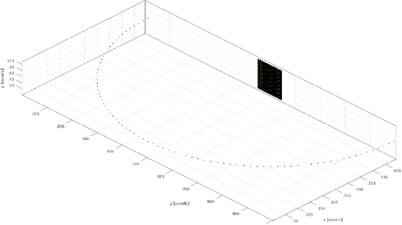
Also, in Advanced Design System (ADS) (Keysight Technologies, Santa Rosa, CA, USA) and k-wave simulations, fabrication limitations are considered. The grid sizes in k-wave are set to 32 µm for 7.5 MHz simulations. The drawback of having smaller grid size is the increasing computational power. As the grid size gets smaller, the computational area for simulation cannot be infinitely large and also for having computational grid size more than 1024 grids results in very long simulation run times. However, having larger grid sizes result in false results. Similar specifications are chosen for 18.5 MHz design and explained in Chapter 3.7 Radiation Pattern Simulations.
Also for the ADS, gap height, tg, is set to 138 nm. However, in fabrication it
is already known that having such a precise resolution in depth is not feasible but for compactness and completeness gap height is taken as the calculated value in Chapter 2.
20
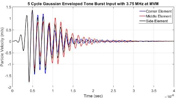
Another consideration in simulations was the presence of Rayleigh-Bloch waves in this CMUT array. Since the size of the array is much larger than the operating wavelength, Rayleigh-Bloch waves come to exist as explained in [26]. Presence and analysis of these spurious waves are also discussed.
Lastly, through this chapter, since presenting the results for each 256 element is not possible, some important portions of results are presented. Elements where major changes can be seen are shown, such as the corner (1st element), side (128th element) and middle (120th element) elements are shown. The differences are mostly caused by the mutual radiation impedance and effect of the rigid baffle around the elements.
Figure 3.1: Orientation and placement of the elements that will be analysed through this work.
In Figure 3.2 the whole simulation flow is explained. In this work, ADS and MATLAB is used coherently and recursively. All of the output signals are obtained by ADS according to the designed transducer specifications and these output signals are used for beamforming and radiation pattern analysis in
1st Element: Corner 120nd Element: Middle 128nd Element: Side
21
MATLAB. Also the delay calculations are made in MATLAB and fed into ADS for beamforming simulations. Further details are explained in corresponding sections.
Figure 3.2: Simulation flow diagram
3.2 Harmonic Balance Analysis
The highly nonlinear nature of this operation mode needs to be inspected through a nonlinear analysis tool. Since the lumped element model is constructed in a conventional circuit simulator like ADS, harmonic balance analysis can be done for nonlinear operations.
For 7.5 MHz transducer, frequency is swept from 1 MHz to 15 MHz with 50 kHz step sizes. Second harmonic of the resulting harmonic balance output is presented in order to analyse the frequency domain output of this transducer. Since the phase difference of force outputs between the elements in the array is negligible, magnitude of the force is used to calculate the pressure outputs of the transducer. Similarly, frequency axis is the second harmonic of the sweep frequency. Resulting frequency domain outputs are shown for AC input voltage of 75 volts and zero DC voltage. According to the results, 232.8 dB re 1µPa pressure is obtained at the operation frequency, 7.5 MHz.
22
Figure 3.3: Second harmonic results of harmonic balance analysis driven with 75 volts AC voltage and zero DC bias for 7.5 MHz transducer.
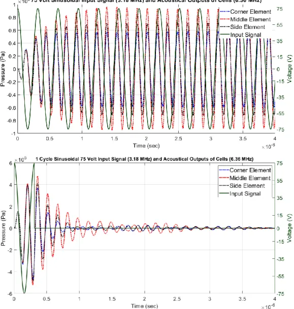
Apart from the operation frequency, peak at 6.36 MHz with 240.6 dB re 1µPa is observed. However, due to the narrow bandwidth structure, this peak is not considered as the resonance frequency in this work. Instead this frequency is called as the peak frequency. Due to the undesirable properties in transient response at this frequency, it is decided to select the operation frequency of 7.5 MHz at the right side of this peak.
Using lumped-element modelling provides the ability of simulating arrays with large number of elements. Unlike FEM, formation of spurious resonances and non-uniformities can be observed and resulted with this method. Given that results obtained by harmonic balance analysis shows the presence of resonances at lower frequencies than the operation or peak frequency of the designed transducer where the Rayleigh-Bloch waves are excited on the surface of the transducer. Presence of Rayleigh-Bloch waves indicate the nonuniformity among cell velocities of the array elements mainly due to the unequal radiation resistance impedance seen by the cells, which can be seen in Figure 3.6. Although these waves do not result in a significant degradation on the point spread function but the oscillations that can be observed in time domain analysis, limits the dynamic range and extends the duration of the impulse
![Figure 2.1: Cross-sectional view of circular CMUT and its clamped membrane deflection structure [29]](https://thumb-eu.123doks.com/thumbv2/9libnet/5687284.114736/30.892.201.762.593.767/figure-cross-sectional-circular-clamped-membrane-deflection-structure.webp)