a dissertation submitted to
the department of physics
and the institute of engineering and science
of bilkent university
in partial fulfillment of the requirements
for the degree of
doctor of philosophy
By
Cem Sevik
January, 2008
Assist. Prof. Dr. Ceyhun Bulutay(Supervisor)
I certify that I have read this thesis and that in my opinion it is fully adequate, in scope and in quality, as a dissertation for the degree of doctor of philosophy.
Prof. Dr. Atilla Aydınlı
I certify that I have read this thesis and that in my opinion it is fully adequate, in scope and in quality, as a dissertation for the degree of doctor of philosophy.
Prof. Dr. Ra¸sit Turan
Assoc. Prof. Dr. Resul Eryi˘git
I certify that I have read this thesis and that in my opinion it is fully adequate, in scope and in quality, as a dissertation for the degree of doctor of philosophy.
Assoc. Prof. Dr. O˘guz G¨ulseren
Approved for the Institute of Engineering and Science:
Prof. Dr. Mehmet B. Baray Director of the Institute
GERMANIUM NANOCRYSTALS
Cem Sevik PhD. in Physics
Supervisor: Assist. Prof. Dr. Ceyhun Bulutay January, 2008
This is a computational work on the Si and Ge nanocrystals (NCs) embedded in wide band gap host matrices. As the initial task, extensive ab initio work on the structural and electronic properties of various NC host matrices, namely, SiO2, GeO2, Si3N4, and Al2O3 are preformed. The structural parameters, elastic
constants, static and optical dielectric constants are obtained in close agreement with the available results. Furthermore, recently reported high density cubic phase of SiO2 together with GeO2 and SnO2 are studied and their stable
high-dielectric constant alloys are identified.
Based on the ab initio study of host matrices, two related high field phenom-ena, vital especially for the electroluminescence in Si and Ge NCs, are examined. These are the hot carrier transport through the SiO2 matrix and the subsequent
quantum-confined impact ionization (QCII) process which is responsible for the creation of electron-hole pairs within the NCs. First, the utility and the validity of the ab initio density of states results are demonstrated by studying the high field carrier transport in bulk SiO2 up to fields of 12 MV/cm using the ensemble
Monte Carlo technique. Next, a theoretical modeling of the impact ionization of NCs due to hot carriers of the bulk SiO2 matrix is undertaken. An original
expression governing the QCII probability as a function of the energy of the hot carriers is derived.
Next, using an atomistic pseudopotential approach the electronic structures for embedded Si and Ge NCs in wide band-gap matrices containing several thou-sand atoms are employed. Effective band-gap values as a function of NC diameter reproduce very well the available experimental and theoretical data. To further check the validity of the electronic structure on radiative processes, direct photon
emission rates are computed. The results for Si and Ge NCs as a function of diameter are in excellent agreement with the available ab initio calculations for small NCs.
In the final part, non-radiative channels, the Auger recombination (AR) and carrier multiplication (CM) in Si and Ge NCs are investigated again based on the atomistic pseudopotential Hamiltonian. The excited electron and excited hole type AR and CM and biexciton type AR lifetimes are calculated for different sized and shaped NCs embedded in SiO2 and Al2O3. Asphericity is also observed
to increase the AR and CM rates. An almost monotonous size-scaling and sat-isfactory agreement with experiment for AR lifetime is obtained considering a realistic interface region between the NC core and the host matrix. It is further shown that the size-scaling of AR can simply be described by slightly decreas-ing the established bulk Auger constant for Si to 1.0×10⁻³⁰cm6s−1. The same
value for germanium is extracted as 1.5×10⁻³⁰cm6s−1 which is very close to the established bulk value. It is further shown that both Si and Ge NCs are ideal for photovoltaic efficiency improvement via CM due to the fact that under an optical excitation exceeding twice the band gap energy, the electrons gain lion’s share from the total excess energy and can cause a CM. Finally, the electron-initiated CM is predicted to be enhanced by couple orders of magnitude with a 1 eV of excess energy beyond the CM threshold leading to subpicosecond CM lifetimes.
Keywords: Si and Ge Nanocrystals, High-Field Transport, Radiative Recombina-tion, Auger RecombinaRecombina-tion, Carrier MultiplicaRecombina-tion, Quantum Confined Impact Ionization, Electronic Structure, High-k Oxides.
S˙IL˙ISYUM VE GERMANYUM NANO ¨
ORG ¨
ULERDE
TAS
¸IYICI D˙INAMI ˘
G˙I
Cem Sevik Fizik, Doktora
Tez Y¨oneticisi: Yard. Do¸c. Dr. Ceyhun Bulutay Ocak, 2008
Bu ¸calı¸sma, Si ve Ge nano¨org¨ulerin (N ¨O’lerin) sayısal hesaplamaları hakkındadır. Ba¸slangı¸c olarak SiO2, GeO2, Si3N4, Ge3N4 ve Al3O3 gibi N ¨O matrislerinin
elek-tronik ve yapısal ¨ozellikleri temel prensipler y¨ontemiyle incelenmi¸stir. Bunun sonucunda, yapısal ¨ozellikler, elastik sabitler, statik ve optik dielektrik sabitler i¸cin mevcut ¸calı¸smalar ile olduk¸ca uyumlu de˘gerler elde edilmi¸stir. Ayrıca, SiO2’nun hen¨uz yayımlanmı¸s y¨uksek yo˘gunluklu k¨ubik fazı GeO2 ve SnO2 da ele
alınarak calı¸sılmı¸s ve bu malzemelerin y¨uksek dielektrik sabitli duragan ala¸sım formları elde edilmi¸stir.
N ¨O matrisleri hakkındaki temel ilkeler hesaplamalarına dayanarak, Si ve Ge N ¨O’lerdeki elektronı¸sıması i¸cin olduk¸ca ¨onemli olan iki y¨uksek elektrik alan olgusu incelenmi¸stir. Bu olgular, SiO2 matrisi i¸cerisinde y¨uksek enerjili y¨uk ta¸sınımı ve
N ¨O i¸cinde elektron-de¸sik ¸ciftlerinin olu¸sumunda rol¨u olan kuvantum tuzaklı darbe iyonizasyonudur (KTDI). ˙Ilk olarak, temel ilkeler y¨ontemiyle hesaplanmı¸s durum yo˘gunluklarının ge¸cerlili˘gini ve yararlılı˘gını test etmek amacı ile SiO2 y¨uksek
en-erjili tasıyıcı ta¸sınımı 12 MV/cm elektrik alan de˘gerine kadar Toplu Monte Carlo y¨ontemi ile tetkik edilmi¸stir. Daha sonra, yı˘gık SiO2 i¸cerisindeki y¨uksek enerjili
ta¸sıyıcılar tarafından tetiklenen N ¨O darbe iyonizasyonunun teorik bir modellemesi ele alınmı¸stır. Neticede, N ¨O i¸cerisinde KTDI oranını y¨uksek enerjili ta¸sıyıcıların enerjisinin bir fonksiyonu olarak veren orjinal bir ifade t¨uretilmi¸stir.
Daha sonra, geni¸s-bant aralıklı yarıiletkenler i¸cerisine g¨om¨ul¨u, birka¸c bin atomdan olu¸san, Si ve Ge N ¨O’lerin elektronik yapısı atomistik g¨or¨un¨urpotansiyel y¨ontemi ile ¸calı¸sılmıstır. N ¨O ¸capının fonksiyonu olarak hesaplanmı¸s etkin bant aralı˘gı de˘gerlerinin mevcut deneysel ve teorik sonu¸clar ile olduk¸ca uyumlu oldu˘gu g¨or¨ulm¨u¸st¨ur. Elektronik yapının radyasyonlu ı¸sıma ¨uzerindeki etkisini belirlemek
amacı ile direk foton yayma oranları hesaplanmı¸s ve hem Si hem de Ge i¸cin mev-cut temel ilkeler veriler ile son derece benzer sonu¸clar elde edilmi¸stir.
N ¨O’n¨un ¸cekirdek b¨olgesi ile matris arasındaki aray¨uz¨un ger¸cek¸ci bir ¸sekilde modellenmesi, yarı¸capa g¨ore neredeyse yeknesak artan ve deney ile hemen hemen uyumlu sonu¸clar elde etmemizi sa˘glamı¸stır. Ayrıca, Si N ¨O’ler i¸cin yarı¸capa g¨ore Auger geribirle¸simi ya¸sam s¨uresi’nin, yı˘gık ¨org¨u Auger sabitini 1.0×10⁻³⁰cm6s−1 alarak basit bir ¸sekilde elde edilebilece˘gi g¨osterilmi¸s ve Ge i¸cin
bu de˘ger 1.5×10⁻³⁰cm6s−1 olarak saptanmı¸stır. N ¨O bant aralı˘gından iki kat
fa-zla optik aydınlatma altında, elektronların uyarma enerjisinin arslan payını alarak iletkenlik bandına ge¸cti˘gi saptanmı¸s ve bu elektronların tetikledi˘gi ta¸sıyıcı katlan-ması ya¸sam s¨urelerinin hesaplanması sonucunda, bu iki N ¨O’nun fotovoltaik uygu-lamalarda verimlili˘gi arttırma ama¸clı kullanımının ¸cok uygun oldu˘gu g¨ozlenmi¸stir. Son olarak, uyarılma enerjisinin e¸sik de˘gerinin yanlızca 1 eV ¨uzerinde TK oranının olduk¸ca y¨ukseldi˘gi ve ya¸sam s¨uresinin birka¸c-picosaniye de˘gerlerine kadar ger-iledi˘gi g¨or¨ulm¨u¸st¨ur.
Anahtar s¨ozc¨ukler: Si ve Ge Nano¨org¨uleri, Y¨uksek Elektrik Alanı Altında Ta¸sınım, Radyasyonlu I¸sıma, Auger Geribirle¸simi, Ta¸sıyıcı Katlanması, Kuvan-tum Tuzak Darbe ˙Iyonizasyonu, Elektronik Yapı, Y¨uksek-k Oksitler.
I would like to express my gratitude to my supervisor Assist. Prof. Dr. Ceyhun Bulutay for not only his instructive comments in the supervision of my thesis but also constitutive contrubution to my life and my personality.
I would like to thank Prof. R. Eryi˘git, T. G¨urel, Prof. O. G¨ulseren, D. C¸ akır and Dr. T. Yıldırım for their useful advices for ab initio studies. This work has been supported by the European FP6 Project SEMINANO with the con-tract number NMP4 CT2004 505285 and by the Turkish Scientific and Technical Council T ¨UB˙ITAK with the project number 106T048. The computations were performed in part by the TR-Grid e-Infrastructure Project of T ¨UB˙ITAK.
I would also like to thank to Prof. Ra¸sit Turan and Prof. Atilla Aydınlı for their useful supports during the SEMINANO project.
I am very happy and proud of making wonderful friends in Bilkent University, I will always remember them.
I am very grateful for my wife Olcay, for her love and patience during the PhD period.
1 Introduction 1
1.1 This Work . . . 3
2 Ab initio Study of the NC Host Crystals 5 2.1 Ab initio study of the nanocrystal host crystal lattices . . . 6
2.1.1 Introduction . . . 6
2.1.2 Details of Ab initio Computations . . . 9
2.1.3 First-principles Results . . . 10
2.2 High-dielectric constant and wide band gap inverse silver oxide phases of the ordered ternary alloys of SiO2, GeO2 and SnO2 . . . 23
2.2.1 Introduction . . . 23
2.2.2 Computational Details . . . 24
2.2.3 Results . . . 25
3 Modeling of the Hot Carrier Transport 32 3.1 Introduction . . . 33
3.1.1 Theoretical Details . . . 34
3.1.2 High Field Transport Results . . . 38
4 Energy Spectra and Radiative Recombination 42 4.1 Introduction . . . 42
4.2 Theory: Energy Spectrum . . . 44
4.3 Theory: Radiative Recombination . . . 46
4.4 Results . . . 47
5 Auger and Carrier Multiplication in NCs 50 5.1 Introduction . . . 51
5.2 Theory . . . 52
5.3 Results . . . 55
6 Conclusions 62 A Bulk Carrier-Initiated NC Impact Ionization 76 A.0.1 Quantum-Confined Impact Ionization . . . 76
A.0.2 Multiplication Process . . . 82
A.0.3 Direct Tunnelling . . . 88
B More on Auger and Carrier Multiplication 89 B.0.4 Auger Recombination in Bulk Systems . . . 89
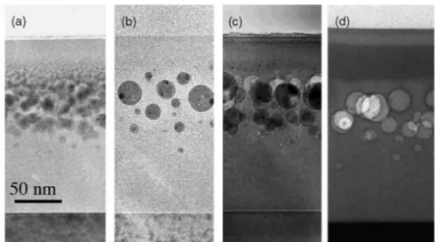
1.1 TEM micrographs of SiO2films implanted with a fluence of 1×10¹⁷
Ge ions cm−2 after annealing for at 1000 ◦C for (a) 15 min, (b)
30 min, (c) 45 min and (d) 60 min, obtained by E. S. Marstein et al.[18] . . . 2
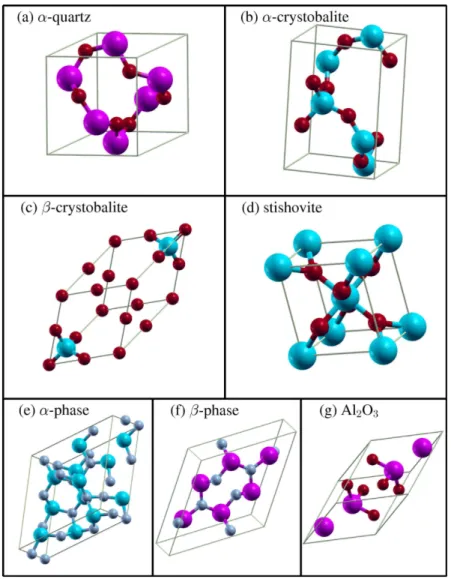
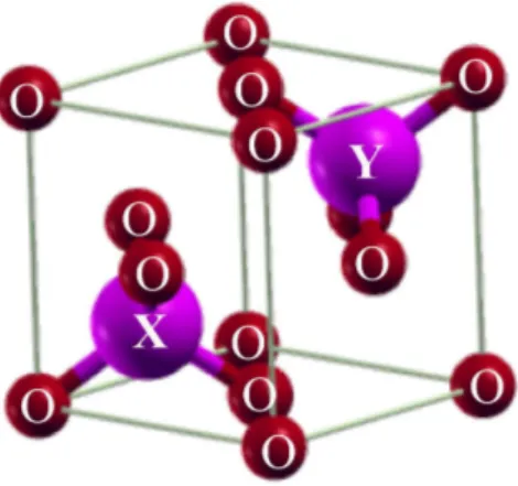
2.1 Ball and stick model of (a) α-quartz XO2, (b) α-crystobalite XO2,
(c) β-crsytobalite XO2, (d) stishovite XO2, (e) α-phase X3N4, (f)
β-phase X3N4, and (g) Al2O3. X refers to Si or Ge. . . 7
2.2 LDA band structure and total DOS (electrons/eV cell) of (a) α-cristobalite SiO2, (b) α-quartz SiO2, (c) β-cristobalite SiO2, and
(d) stishovite SiO2. . . 15
2.3 DOS of α-quartz SiO2 (a) Element-resolved; total, PDOS of Si,
PDOS of O. (b) Angular momentum-resolved; Si s electrons, Si p electrons, Si d electrons (not visible at the same scale), O s electrons, O p electrons. . . 16 2.4 LDA band structure and total DOS of (a) α-quartz GeO2, (c) rutile
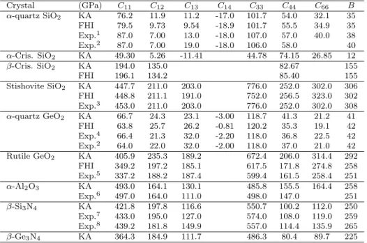
GeO2. . . 17
2.5 DOS of rutile GeO2 (a) Element-resolved; total PDOS of Ge,
PDOS of O. (b) Angular momentum-resolved; Ge s electrons, Ge p electrons, Ge d electrons, O s electrons, O p electrons. . . 18
2.6 LDA band structure of and total DOS of α-Al2O3. . . 19
2.7 LDA band structure and total DOS of (a) α-Si3N4, (b) β-Si3N4,
(c) α-Ge3N4 and (d) β-Ge3N4. . . 21
2.8 Element-resolved DOS of (a) β-Si3N4; total, PDOS of Si, PDOS of
N, (b) β-Ge3N4; total, PDOS of Ge, PDOS of N. . . 22
2.9 Density versus direction-averaged static electric susceptibility. . . 22 2.10 Ball and stick model of the i-phase ordered ternary alloy X0.5Y0.5O2. 24
2.11 LDA phonon dispersions of the unstable crystals: (a) GeO2, (b) SiO2. 27
2.12 LDA phonon dispersions and the phonon DOS (a. u.) of the stable crystals: (a) SiO2, (b) Ge0.5Si0.5O2, (c) Ge0.5Sn0.5O2, and
(d) Si0.5Sn0.5O2. . . 28
2.13 LDA electronic band structure and DOS (States/eV cell) of i-phase (a) SiO2, (b) Ge0.5Si0.5O2, (c) Ge0.5Sn0.5O2, and (d) Sn0.5Si0.5O2. . 29
3.1 Quantum-confined impact ionization in NCs. . . 33 3.2 Pseudopotential and the fitted hydrogenic wave functions. . . 37 3.3 QCII probability for carrier densities; 1014 cm−3, 1015 cm−3, and
1016 cm−3. . . . 38
3.4 For SiO2 (a) average velocity vs field (b) field vs energy profiles for
both electrons and holes. . . 39 3.5 Temporal evolution of the ensemble-averaged (a) electron energy
and (b) average velocity for different electric field values. . . 40 3.6 For SiO2 (a) field vs energy, (b) energy vs time and (c) average
4.1 Pseudopotential atomistic energy spectra of Si and Ge NCs for different diameters. The dashed lines indicate the conduction band minimum and valence band maximum for the bulk semiconductors. 47 4.2 The variation of the radiative lifetime with respect to diameter for
Si and Ge NCs. Our data is compared with the existing ab initio and tight-binding results in the literature. . . 48
5.1 Auger recombination and carrier multiplication in nanocrystals. . 53 5.2 (a) Embedded NC in a supercell, core atoms of a (b) spherical, (c)
oblate and (d) prolate ellipsoidal NC. . . 54 5.3 Smeared interface of Nanocrystals. . . 55 5.4 AR lifetimes for (a) excited electron, (b) excited hole, and (c)
biex-citon types in Si NCs, and (d) excited electron, (e) excited hole, and (f) biexciton types in Ge NCs. Square symbols represent AR lifetimes with interface smearing, and dashed lines show AR life-times calculated from our proposed C values. Spherical symbols in (a) and (b) represent AR lifetimes in Si NCs with abrupt interfaces. 56 5.5 Average Coulomb matrix elements for (a) Si and (b) Ge NCs for
EE type AR (red squares) and for EH type AR (black spheres). . 58 5.6 Final state configuration for, (a) AR in Si, (b) AR in Ge, (c) CM in
Si and (d) CM in Ge NCs. Dashed line in (a) and (b) corresponds to exact conserved energy . . . 59 5.7 CM Lifetime results for (a) EE and (b) EH types in Si NCs
em-bedded in SiO2 and Al2O3, and (c) EE and (d) EH types in Ge
NCs embedded in Al2O3. . . 60
5.8 (a) Electron and hole excess energy vs pump energy for 4 nm Si and 3 nm Ge NCs, (b) CM lifetime vs electron excess energy for different diameter of Si and Ge NCs. . . 61
A.1 A schematic illustration of the (a) QCII, (b) multiplication and (c) direct tunnelling processes in nanocrystals. . . 77
2.1 Structural information on crystals. . . 11 2.2 Bond lengths and bond angles (in degrees) of SiO2 and GeO2
poly-morphs where x represents a Si or a Ge atom. . . 12 2.3 Elastic constants and bulk modulus for each crystal. . . 13 2.4 Dielectric permittivity tensor. . . 14 2.5 Indirect (Eg) and direct (Eg(Γ)) LDA Band Gaps for each crystal. 14
2.6 First-principles LDA and GGA structural data for i-phase crystals. 25 2.7 Elastic constants and bulk modulus for each crystal. . . 26 2.8 LDA and GGA dielectric permittivity tensor for the stable crystals. 27 2.9 Indirect (Eg) and direct (Eg,Γ) band gaps for each i-phase crystal
within LDA, GGA, and for the stable structures the GW approx-imation (GWA). . . 30
5.1 AR lifetimes for different ellipsoidal shapes of Si NCs with diame-ters of 1.63 and 2.16 nm. . . 57 5.2 Comparison of AR lifetimes for SiO2 and Al2O3 host matrices. . . 58
Introduction
Due to its indirect band gap bulk silicon is a very inefficient emitter, even at liquid helium temperatures. Within the last decade several approaches were developed towards improving the efficiency of light emission from Si-based structures. In spirit, all were based on the lifting of the lattice periodicity that introduces an un-certainty in the k-space and therefore altering the indirect nature of this material. Some examples are: SiGe or Si-SiO2 superlattices [1, 2] or Si nanocrystal (NC)
assemblies [3] (see Fig. 1.1). Recently, intensive electroluminescence (EL) from Si implanted SiO2 [4] and Si implanted sapphire [5] layers were observed. Besides,
EL from Ge-implanted SiO2[6, 7] layers and Ge implanted SiNx[8] layers were also
predicted. Applications of NC-based structures in laser emitters, [9, 10, 11, 12] EL devices, [13, 14] switching elements, [15] and solar batteries [16] have been announced in the recent past. Moreover, the search for new-generation photo-voltaics has gained momentum and hence the subject of direct photon absorption in NCs [17] is of prime interest. The largest quantum yield that has been achieved under optical excitation of Si NCs is of the order of 50% and is already comparable with that of direct band-gap quantum dots assemblies.
In spite of these exciting properties of NCs, their transport and emission mechanisms are still unclear. A theoretical understanding of these exciting prop-erties first of all requires a detailed and accurate electronic structure tool which can then be used to predict certain optoelectronic properties as well as other
Figure 1.1: TEM micrographs of SiO2 films implanted with a fluence of 1×10¹⁷
Ge ions cm−2after annealing for at 1000◦C for (a) 15 min, (b) 30 min, (c) 45 min
and (d) 60 min, obtained by E. S. Marstein et al. [18]
quantum processes such as quantum confined impact ionization (QCII), Auger recombination (AR) and carrier multiplication (CM). However, such a task be-comes formidable in the case of NCs: the ab initio approaches [19] are currently out of consideration as there are 1,000-20,000 atoms within the active region of these structures. On the other hand the standard multiband k·p approaches [20] are neither accurate for NCs nor applicable directly to indirect band-gap semi-conductors such as in Si and Ge based NCs. Based on these facts, the most useful method to search NCs is the recently proposed linear combination of bulk bands (LCBB) recipe by the Zunger group from NREL (USA) [21, 22]. The LCBB has been used for self-assembled quantum dots [23, 22], superlattices [24, 25] and high-electron mobility transistors [26], and very recently on the aggregation of Si NCs [27].
Quantum processes such as radiative recombination, QCII, AR and CM have strong effect on carrier dynamics, emission and absorption mechanisms in NCs. One of the most important one especially responsible for exciton generation in quantum dots and NCs is the QCII. This process is responsible for the intro-duction of confined excitons in silicon NC devices which is a key luminescence
mechanism. Another important processes AR and CM are responsible for the nonradiative annihilation and creation of confined excitons in NCs. The rate of these two processes affects many aspects of the performance of nanoscale devices. The latter has been demonstrated in a very recent experimental study by signif-icantly increasing the solar cell efficiency in colloidal Si NCs due to CM which enables multiple exciton generation in response to a single absorbed photon [28]. Similarly, the inverse process, AR is also operational and it introduces a com-peting mechanism to CM which can potentially diminish the solar cell efficiency and in the case of light sources it degrades the performance by inflating the nonradiative carrier relaxation rate [29]. A recent paper by Troj´anek et al. [30] reports that the photoluminescense decay time for Si NC is about 105 ps. This is the characteristic time scale for the nonradiative AR process. As it is signif-icantly shorter than the time of the radiative emission (approximately 20 to 30 nanoseconds [31, 32]), its main implication is that AR should inhibit the NC laser, LED operations. Without any doubt, it is also detrimental for solar cell applications as the created electron-hole pairs disappear without contributing to the photocurrent.
1.1
This Work
Aiming for a clear and realistic characterization of the fundamental processes such as QCII, AR and CM in embedded Si and Ge NCs, first we start with the ab initio calculations of electronic and structural properties of the NC host matrices. Our analysis includes wide band-gap crystalline oxides and nitrides such as SiO2 (α-quartz, α- and β-cristobalite and stishovite), GeO2 (α-quartz, and
rutile) Al2O3 (α-phase), Si3N4 (α- and β-phases), and Ge3N4 (α- and β-phases).
Electronic structure and the elastic properties of these important insulating oxides and nitrides are obtained with high accuracy based on density functional theory within the local density approximation. We also perform detailed calculations about new high-k cubic phase of SiO2, GeO2, SnO2 and their ternary alloys. This
part of the thesis work has been published in Journal of Material Science [33], Physical Review B [34] and Materials Sciences in Semiconductor Processing [35].
Next, in Chapter 3, we start by characterizing the hot electron transport in oxides within the ensemble Monte Carlo (EMC) framework including all major scattering mechanism such as acoustic, polar and non-polar optical phonon scat-terings. Afterwards, we derive an analytical expression for the QCII probability in NCs that can become an instrumental result in assessing EL in the presence of other competing scattering mechanisms. The effect of QCII on bulk transport quantities is also discussed. This part of the thesis work has been published in Physica E [36] and Physica Status Solidi C [37].
In Chapter 4, embedded Si and Ge NCs in wide band-gap matrices are studied theoretically using an atomistic pseudopotential approach. From small clusters to large NCs containing on the order of several thousand atoms are considered. The energy spectrum and real-space wavefunctions of each state are produced and employed in the calculation of the AR and CM. For the comparison purposes with the nonradiative processes, radiative recombination lifetime for Si and Ge NCs as a function of diameter are computed. Our results are in excellent agreement with the very reliable ab initio calculations which is only available for small NCs [38]. Finally in Chapter 5, we provide an atomistic theoretical account of CM and AR in embedded Si and Ge NCs which reveals their size, shape and host matrix dependence. Unlike most previous treatments, the NCs are considered to be embedded into different wide band-gap host matrices. The electron- and hole-initiated types of AR and CM and biexciton-type of AR are considered based on an atomistic pseudopotential model. This part of the thesis work has been submitted to Physical Review B as a Rapid Communication.
Chapter 6 contains our conclusions and main achievements in this thesis. The two Appendix sections at the end provide the technical details of the theoretical derivations on the QCII and related bulk carrier-initiated Coulombic excitations and give some background information and further theoretical details on AR in the bulk and NCs. Extensive literature survey on each individual topic is given at the beginning of each chapter. Special emphasis is given to the comparison of our results with the experimental and theoretical data, whenever possible.
Ab initio Study of the
Nanocrystal Host Crystal
Lattices
To completely investigate the electronic and transport properties of embedded Si and Ge nanocrystals (NCs) it is obligatory to have a thorough mastering of the host matrices into which these NCs are embedded. Therefore as a first part of the thesis, we performed an extensive theoretical study for NC host matrices which are wide bandgap crystalline oxides and nitrides, namely, SiO2, GeO2, Al2O3,
Si3N4, and Ge3N4. In addition to the NC host matrices we also considered the
recently reported inverse silver oxide phase of SiO2 that possesses a high dielectric
constant (high-k) as well as lattice constant compatibility to Si. Moreover, we explored the closely-related oxides, GeO2, SnO2 and their alloy formations with
the same inverse silver oxide structure. The details of these two studies are presented in this Chapter collocated as follows: in Sec. 2 we provide details of our ab initio computations and our first-principles results for the structural, electronic properties of the NC host lattices, Sec. 3 includes the same details about high-k inverse silver oxide structures.
2.1
Ab initio study of the nanocrystal host
crys-tal lattices
As the first task of the thesis, we performed an extensive ab initio study for NC host matrices which are wide bandgap crystalline oxides and nitrides, namely, SiO2, GeO2, Al2O3, Si3N4, and Ge3N4. Their important polymorphs are
con-sidered which are for SiO2: α-quartz, α- and β-cristobalite and stishovite, for
GeO2: α-quartz, and rutile, for Al2O3: α-phase, for Si3N4 and Ge3N4: α- and
β-phases (see Fig. 2.1). This Chapter presents a comprehensive account of both electronic structure and the elastic properties of these important insulating ox-ides and nitrox-ides obtained with high accuracy based on density functional theory within the local density approximation. Two different norm-conserving ab initio pseudopotentials have been tested and shown to agree in all respects with the only exception arising for the elastic properties of rutile GeO2. The agreement
with experimental values, when available, is seen to be highly satisfactory. The uniformity and the well convergence of this approach enable an unbiased assess-ment of important physical parameters within each material and among different insulating oxide and nitrides. The computed static electric susceptibilities are observed to display a strong correlation with their mass densities. There is a marked discrepancy between the considered oxides and nitrides with the latter having sudden increase of density of states away from the respective band edges. This is expected to give rise to excessive carrier scattering which can practically preclude bulk impact ionization process in Si3N4 and Ge3N4.
2.1.1
Introduction
Insulating oxides and nitrides are indispensable materials for diverse applications due to their superior mechanical, thermal, chemical and other outstanding high temperature properties. Furthermore, in the electronic industry these wide band gap materials are being considered for alternative gate oxides [39] and in the field of integrated optics they provide low-loss dielectric waveguides [40]. Recently the subject of wide bandgap oxides and nitrides have gained interest within the
context of nanocrystals which offer silicon-based technology for light emitting devices and semiconductor memories [14]. These nanocrystals are embedded in an insulating matrix which is usually chosen to be silica [41, 42, 43, 44]. However, other wide bandgap materials are also employed such as germania [45, 46], silicon nitride [47, 48, 49], and alumina [50, 51, 52]. As a matter of fact, the effect of different host matrices is an active research topic in this field.
Figure 2.1: Ball and stick model of (a) α-quartz XO2, (b) α-crystobalite XO2,
(c) β-crsytobalite XO2, (d) stishovite XO2, (e) α-phase X3N4, (f) β-phase X3N4,
and (g) Al2O3. X refers to Si or Ge.
ones are SiO2, Al2O3, Si3N4. The activity around GeO2 is steadily increasing.
Another closely-related material, Ge3N4 has attracted far less attention up to
now even though it has certain interesting properties [53]. The major obstacle has been the sample growth. However, a very recent study reported an in situ Ge3N4 growth on Ge, demonstrating high thermal stability and large band offsets
with respect to the Ge system [54]. In our comprehensive treatment, we present the ab initio structural and electronic properties of all these materials considering their common polymorphs; these are for SiO2: α-quartz, α- and β-cristobalite and
stishovite phases, for GeO2: α-quartz, and rutile phases, for Si3N4 and Ge3N4:
α-and β-phases α-and for Al2O3: α-phase. For amorphous and inherently imperfect
matrices, these perfect crystalline phases serve as important reference systems. Moreover, due to their distinct advantages, epitaxial host lattices are preferred over the amorphous ones for specific applications.
With an eye on these technological applications, we focus on several physical properties of these lattices. The elastic constants play an important role on the strain profile of the embedded core semiconductor. Using Eshelby’s continuum elastic consideration [55] the radial and tangential stress fields of the nanocrys-tal can be determined [56]; these in turn, affect the optical properties [43]. The static and optical dielectric constants of these lattices introduce nontrivial local field effects that modify the absorption spectra of an isolated nanocrystal when embedded inside one of these matrices [57]. Based on the simple effective medium theory which has been tested by ab initio calculations [58], one can assess which host lattice and nanocrystal combination would possess the desired optical prop-erties. Because of the dielectric mismatch between the nanocrystal core and the surrounding lattice, image charges will be produced [59]. These image charges should be taken into account in characterizing nanocrystal excitons [3]. Another promising application is the visible and near infrared electroluminescence from Si and Ge nanocrystals [14]. The electroluminescence is believed to be achieved by the recombination of the electron hole pairs injected to nanocrystals under high bias [14]. In this context the bulk state impact ionization process which can also give rise to electroluminescence is considered to be detrimental leading to dielectric breakdown.
For high-field carrier transport, the crucial physical quantity was identified to be the valence and conduction band density of states (DOS) for each of the crystalline polymorph [60]. Based on these technology-driven requirements we compute the elastic constants, band structures, dielectric permittivities and elec-tronic DOS of these aforementioned crystal polymorphs. Our ab initio framework is based on the density functional theory [61, 62], using pseudopotentials and a plane wave basis [19]. With the exception of Ge3N4 which was far less studied,
vast amount of theoretical work is already available spread throughout the lit-erature based on a variety of techniques [63, 64, 65, 66, 67, 68, 69, 70, 71, 72]. Our first-principles study here enables a uniform comparison of important phys-ical parameters within each material and among different insulating oxides and nitrides.
2.1.2
Details of
Ab initio Computations
Structural and electronic properties of the polymorphs under consideration have been calculated within the density functional theory [61, 62], using the plane wave basis pseudopotential method as implemented in the ABINIT code [19]1.
The results are obtained under the local density approximation (LDA) where for the exchange-correlation interactions we use the Teter-Pade parameterization [73], which reproduces Perdew-Zunger [74] (which reproduces the quantum Monte Carlo electron gas data of Ceperley and Alder [75]). We tested the results under two different norm-conserving Troullier and Martins [76] type pseudopotentials, which were generated by A. Khein and D.C. Allan (KA) and Fritz Haber Institute (FHI). For both pseudopotentials, the valence configurations of the constituent atoms were chosen as N(2s2p3), O(2s2p4), Al(3s23p1), Si(3s23p2), and Ge(4s24p2).
The number of angular momenta of the KA (FHI) pseudopotentials and the chosen local channel were respectively, for N: 1, p (3, d), for O: 1, p (3, d), for Al: 2, d (3, d), for Si: 2, d (3, d), and for Ge: 1, p (3, s). Our calculated values for these two types of pseudopotentials were very similar, the only exceptional case being the elastic constants for rutile GeO2. Dielectric permitivity and the
fourth-order tensor of elastic constants of each crystal are determined by starting from relaxed unit cell under the application of finite deformations within density functional perturbation theory [77] as implemented in ABINIT and ANADDB extension of it. Another technical detail is related with the element- and angular momentum-resolved partial density of states (PDOS). To get a representative PDOS behavior we need to specify the spherical regions situated around each relevant atomic site. The radii of these spheres are chosen to partition the bond length in proportion to the covalent radii of the constituent atoms. This resulted in the following radii: for the α-quartz SiO2, rSi = 0.97 ˚A, rO = 0.65 ˚A, for
the rutile GeO2, rGe = 1.16 ˚A, rO = 0.69 ˚A, for the α-Al2O3, rAl = 1.32 ˚A,
rO = 0.56 ˚A, and for the β-Si3N4, rSi = 1.03 ˚A, rN = 0.70 ˚A. It should be
pointed that even though such an approach presents a good relative weight of the elements and angular momentum channels, it inevitably underestimates the total DOS, especially for the conduction bands. Other details of the computations are deferred to the discussion of each crystal polymorph.
2.1.3
First-principles Results
First, we address the general organization and the underlying trends of our re-sults. The lattice constants and other structural informations of all crystals are listed in Table 2.1. Table 2.2 contains the bond lengths and bond angles of the optimized oxide polymorphs. These results can be used to identify the represen-tation of each polymorph within the amorphous oxides [78]. The elastic constants and dielectric permittivity tensor of each crystal are tabulated in Table 2.3 and Table 2.4, respectively. Very close agreement with the existing experimental data and previous calculations can be observed, which gives us confidence about the accuracy and convergence of our work. Employing KA pseudopotentials, the band structure for the crystals are displayed along the high-symmetry lines in Figs. 2.2, 2.4, 2.6, 2.7 together with their corresponding total DOS. Such an information is particlulary useful in the context of high-field carrier transport. These results are in good agreement with the previous computations [64, 71, 70, 67]. For all
Table 2.1: Structural information on crystals.
Crystal Crystal Lattice Constants (˚A) Space Group Molecules Per Density
Structure Prim. Cell (gr/cm3)
α-quartz SiO2 Hexagonal a =4.8831 4.85424.9133 P 3221 3 2.698
c =5.3711 5.3412 5.4053
α-cris. SiO2 Tetragonal a =4.9501 4.93924.9733 P 41212 4 2.372
c =6.9091 6.8942 6.9263
β-cris. SiO2 Cubic a =7.4031 7.33027.1603 F d3m 2 1.966
Stishovite SiO2 Tetragonal a =4.1751 4.14524.1794 P 42/mnm 2 4.298
c =2.6621 2.6432 2.6654
α-quartz GeO2 Hexagonal a =4.8701 4.86124.9846 P 3221 3 4.612
c =5.5341 5.5202 5.6606
Rutile GeO2 Tetragonal a =4.2831 4.31424.40667 P 42/mnm 2 6.655
Tetragonal c =2.7821 2.8042 2.86197 α-Al2O3 Rombohedral a =4.7581 4.7625 R3c 2 3.992 c =12.981 12.8965 α-Si3N4 Hexagonal a =7.7321 7.7669 C3v4 4 3.211 c =5.6031 5.6159 β-Si3N4 Hexagonal a =7.5801 7.58510 C62h 2 3.229 c =2.8991 2.89510 α-Ge3N4 Hexagonal a =7.985a C34v 4 5.691 c =5.786a β-Ge3N4 Hexagonal a =7.826a C6h2 2 5.727 c =2.993a aThis Work KA bThis Work FHI cRef. [79] dRef. [80] fRef. [81] gRef. [82, 21] eRef. [66] iRef. [67] jRef. [72]
of the considered polymorphs the conduction band minima occur at the Γ point whereas the valence band maxima shift away from this point for some of the phases making them indirect band gap matrices (see Table 2.5). However, the direct band gap values are only marginally above the indirect band gap values. These LDA band gaps are underestimated which is a renown artifact of LDA for semiconductors and insulators [83]. In this work we do not attempt any correction procedure to adjust the LDA band gap values.
We present in Figs. 2.3, 2.5, 2.8 the element- and angular momentum-resolved PDOS. A common trend that can be observed in these various lattices is that their valence band maxima are dominated by the p states belonging to O atoms; in the case of Si3N4 and Ge3N4 they are the N atoms. For the conduction band
the observation in amorphous SiO2 where due to large electronegativity difference
between Si and O, the bonding orbitals have a large weight on O atoms whereas the lowest conduction band states with antibonding character have a significant contribution from the Si atoms [84].
Table 2.2: Bond lengths and bond angles (in degrees) of SiO2 and GeO2
poly-morphs where x represents a Si or a Ge atom.
Crystal x-O (˚A) x-O (˚A) O-x-O O-x-O O-x-O O-x-O x-O-x x-O-x
α-quartz SiO2 This Work 1.613 1.618 110.75 109.32 109.07 108.47 140.55
Exp.1 1.605 1.614 110.50 109.20 109.00 108.80 143.7
α-quartz GeO2 This Work 1.693 1.699 113.03 110.62 107.94 106.16 130.56
α-cris. SiO2 This Work 1.597 1.596 111.59 110.08 109.03 108.02 146.02
Exp.2 1.603 1.603 111.40 110.00 109.00 108.20 146.5
β-cris. SiO2 This Work 1.603 109.47 180
Exp.3 1.611 107.80 180.00
Stishovite SiO2 This Work 1.804 1.758 98.47 81.53 130.76 98.47
Exp.4 1.760 1.810 130.60
Rutile GeO2 This Work 1.848 1.824 99.34 80.66 99.34 130.33
aRef. [85] bRef. [86] cRef. [87] dRef. [88]
From another perspective, the band structures and the associated DOS reveal that there is a marked discrepancy between the valence and conduction band edges where for the former there occurs a sharp increase of DOS just below the band edge. As the probabilities of most scattering processes are directly proportional to DOS [89], in the case of high-field carrier transport the electrons should encounter far less scatterings and hence gain much higher energy from the field compared to holes. In this respect Si3N4and Ge3N4are further different from
the others where for both conduction and valence bands the DOS dramatically increases (cf. Fig. 2.7) so that the carriers should suffer from excessive scatterings which practically precludes the bulk impact ionization for this material.
Another common trend can be investigated between the density of each poly-morph and the corresponding static permittivity, ǫs. Such a correlation was put
forward by Xu and Ching among the SiO2 polymorphs [64]. We extend this
com-parison to all structures considered in this work and rather use ǫs− 1 = 4πχe
which is propational to the electric susceptibility, χe. It can be observed from
and α-Al2O3.
Table 2.3: Elastic constants and bulk modulus for each crystal.
Crystal (GPa) C11 C12 C13 C14 C33 C44 C66 B α-quartz SiO2 KA 76.2 11.9 11.2 -17.0 101.7 54.0 32.1 35 FHI 79.5 9.73 9.54 -18.9 101.7 55.5 34.9 35 Exp.1 87.0 7.00 13.0 -18.0 107.0 57.0 40.0 38 Exp.2 87.0 7.00 19.0 -18.0 106.0 58.0 40 α-Cris. SiO2 KA 49.30 5.26 -11.41 44.78 74.15 26.85 12 β-Cris. SiO2 KA 194.0 135.0 82.67 155 FHI 196.1 134.2 85.40 155 Stishovite SiO2 KA 447.7 211.0 203.0 776.0 252.0 302.0 306 FHI 448.8 211.1 191.0 752.0 256.5 323.0 302 Exp.3 453.0 211.0 203.0 776.0 252.0 302.0 308 α-quartz GeO2 KA 66.7 24.3 23.1 -3.00 118.7 41.3 21.2 41 FHI 63.8 25.7 26.2 -0.81 120.2 35.3 19.1 42 Exp.4 66.4 21.3 32.0 -2.20 118.0 36.8 22.5 42 Exp.2 64.0 22.0 32.0 -2.00 118.0 37.0 21.0 42 Rutile GeO2 KA 405.9 235.3 189.2 672.4 206.0 314.4 292 FHI 349.2 197.2 185.1 617.5 171.8 274.8 258 Exp.5 337.2 188.2 187.4 599.4 161.5 258.4 251 α-Al2O3 KA 493.0 164.1 130.1 485.8 155.5 164.4 258 Exp.6 497.0 164.0 111.0 498.0 147.0 251 β-Si3N4 KA 421.8 197.8 116.6 550.7 100.2 112.0 250 Exp.7 433.0 195.0 127.0 574.0 108.0 119.0 259 Exp.8 439.2 181.8 149.9 557.0 114.4 135.9 265 β-Ge3N4 KA 364.3 184.9 111.7 486.3 80.4 89.7 225 aRef. [90] bRef. [91] cRef. [92] dRef. [81] eRef. [21] fRef. [93] gRef. [94] hRef. [95]
On the other hand, Ge-containing structures while possessing a similar trend among themselves, display a significant shift due to much higher mass of the this atom. This dependence on the atomic mass needs to be removed by finding a more suitable physical quantity. We should mention that such a correlation does not exist between the volume per primitive cell of each phase and the static permittivity. After these general comments, now we concentrate on the results of each lattice individually.
Table 2.4: Dielectric permittivity tensor. Crystal ǫ0 xx= ǫ0yy ǫ0zz ǫ ∞ xx= ǫ ∞ yy ǫ ∞ zz α-quartz SiO2 4.643 4.847 2.514 2.545 α-cris. SiO2 4.140 3.938 2.274 2.264 β-cris. SiO2 3.770 3.770 2.078 2.078 Stishovite SiO2 10.877 8.645 3.341 3.510 α-quartz GeO2 5.424 5.608 2.864 2.947 Rutile GeO2 10.876 8.747 3.679 3.945 α-Al2O3 10.372 10.372 3.188 3.188 β-Si3N4 8.053 8.053 4.211 4.294 β-Ge3N4 8.702 8.643 4.558 4.667 2.1.3.1 SiO2
The α-quartz SiO2 is one of the most studied polymorphs as it is the stable
phase at ambient pressure and temperature [65, 69], furthermore its short-range order is essentially the same as the amorphous SiO2 [84]. α-quartz SiO2 has a
hexagonal unit cell containing three SiO2 molecules. A plane-wave basis set with
an energy cutoff of 60 Hartree was used to expand the electronic wave functions at the special k-point mesh generated by 10×10×8 Monkhorst-Pack scheme [96]. The band structure of α-quartz SiO2 has been calculated by many authors (see,
for instance [63, 64]). Our calculated band structure and total DOS shown in Fig. 2.2(a) are in agreement with the published studies [64].
Table 2.5: Indirect (Eg) and direct (Eg(Γ)) LDA Band Gaps for each crystal.
Crystal VB Max. CB Min. Eg(eV) Eg(Γ) (eV)
α-quartz SiO2 K Γ 5.785 6.073 α-cris. SiO2 Γ Γ 5.525 5.525 β-cris. SiO2 Γ Γ 5.317 5.317 Stishovite SiO2 Γ Γ 5.606 5.606 α-quartz GeO2 K Γ 4.335 4.434 Rutile GeO2 Γ Γ 3.126 3.126 α-Al2O3 Γ Γ 6.242 6.242 α-Si3N4 M Γ 4.559 4.621 β-Si3N4 A-Γ Γ 4.146 4.365 α-Ge3N4 M Γ 3.575 3.632 β-Ge3N4 A-Γ Γ 3.447 3.530
The indirect LDA band gap for this crystal is 5.785 eV from the valence band maximum at K to the conduction band minimum at Γ. The direct LDA band gap at Γ is slightly larger than the indirect LDA band gap as seen in Table 2.5. Calculated values of the elastic constants and bulk modulus listed in Table 2.3 are in good agreement with the experiments. Apart from C12, the elastic constants are
within 10% of the experimental values. The discrepancy in C12 can be explained
by the fact that C12 is very soft and this type of deviation also exists among
experiments which is also the case for C14.
Figure 2.2: LDA band structure and total DOS (electrons/eV cell) of (a) α-cristobalite SiO2, (b) α-quartz SiO2, (c) β-cristobalite SiO2, and (d) stishovite
SiO2.
The α-cristobalite SiO2 has a tetragonal unit cell containing four SiO2
molecules. In the course of calculations an absolute energy convergence of 10−4Ha
was obtained by setting a high plane wave energy cutoff as 60 Ha and 10×10×8 k-point sampling. Figure 2.2(b) shows the band structure of α-cristobalite SiO2
smallest among all the host lattice polymorphs considered in this work.
Figure 2.3: DOS of α-quartz SiO2 (a) Element-resolved; total, PDOS of Si, PDOS
of O. (b) Angular momentum-resolved; Si s electrons, Si p electrons, Si d electrons (not visible at the same scale), O s electrons, O p electrons.
Regarding β-cristobalite, its actual structure is somewhat controversial, as a number of different symmetries have been proposed corresponding to space groups F d3m, I42d, and P 213 [69]. Recently, incorporating the quasiparticle
corrections the tetragonal I42d phase was identified to be energetically most stable [97]. However, we work with the structure having the space group of F d3m that was originally proposed by Wyckoff [98] and which is widely studied primarily due to its simplicity [63, 65]. This phase has a cubic conventional cell with two molecules. We used 60 Ha plane wave energy cutoff and 10×10×10 k-point sampling. Figure 2.2(c) shows the band structure of β-cristobalite SiO2
with the 5.317 eV direct band gap at Γ. Unlike their band structures, total DOS of α- and and β-cristobalite SiO2 are very similar (cf. Fig. 2.2(c)). This similarity
can be explained by the fact that their local structures are very close. On the other hand there is a considerable difference between the DOS spectra of the α-quartz SiO2and the β-cristobalite SiO2. In Table 2.3, we present elastic constants
of the β-cristobalite SiO2 calculated by two types of pseudopotentials, FHI and
KA. There is no considerable difference between them. Dielectric constants of β-cristobalite SiO2 are the smallest among the five polymorphs of SiO2 studied
here (see Table 2.4).
Figure 2.4: LDA band structure and total DOS of (a) α-quartz GeO2, (c) rutile
GeO2.
Stishovite is a dense polymorph of SiO2 with octahedrally coordinated silicon,
unlike the previous phases [69]. It has a tetragonal cell with two molecules. Calculations were done by using 60 Ha plane wave energy cutoff and 8×8×10 k-point sampling. The band structure of stishovite with a wide single valence band is markedly different from that of the previous three crystalline phases of SiO2 having two narrow upper valence bands. The cause of this increased valence
bandwidth is the lack of separation between bonding and nonbonding states [71]. Hence, the total DOS for stishovite shows no gap at the middle of the valence band (see Fig. 2.2(d)). Our calculations yield a direct LDA band gap of 5.606 eV at Γ. As seen in Table 2.3, the differences between our computed elastic constants and the experimental values are less than 3%; this is an excellent agreement for LDA. Its bulk modulus is the largest among all the host lattice polymorphs considered in this work. Moreover, dielectric constants of stishovite is the largest of the five polymorphs of SiO2 considered in this work (see Table 2.4).
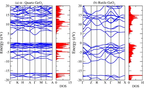
Figure 2.5: DOS of rutile GeO2 (a) Element-resolved; total PDOS of Ge, PDOS
of O. (b) Angular momentum-resolved; Ge s electrons, Ge p electrons, Ge d electrons, O s electrons, O p electrons.
2.1.3.2 GeO2
For α-quartz GeO2 we used the same energy cutoff and k-point sampling as with
α-quartz SiO2, which yields excellent convergence. The band structure of the
α-quartz GeO2 is displayed in Fig. 2.4(a). The similarity of the band structures
of the α-quartz GeO2 and the α-quartz SiO2 is not surprising as they are
isostruc-tural. Similarly their total DOS resemble each other (cf. Fig. 2.4(a)). The indirect LDA band gap for this phase is 4.335 eV from the valence band maximum at K to the conduction band minimum at Γ. The direct band gap at Γ is slightly different from indirect band gap as seen in Table 2.5. This gap is smaller than that of the α-quartz SiO2. The perfect agreement between calculated elastic constants of the
α-quartz GeO2 and experimental values [91, 81] can be observed in Table 2.3.
The rutile structure of GeO2, also known as argutite [99] is isostructural with
the stishovite phase of SiO2. The same energy cutoff and k-point sampling values
for rutile-GeO2 is less than that of stishovite with a value of 3.126 eV. The two
upper valence bands are merged in the total DOS (see Fig. 2.4(b)) as in the case of stishovite. The increased valence bandwidth in the band structure can be explained by the same reason as in the case of stishovite. The results of the elastic constants calculated with KA type pseudopotential shown in Table 2.3 deviate substantially from the experiment whereas the agreement with the FHI pseudopotentials is highly satisfactory. The similarity of the dielectric constants of rutile GeO2 and stishovite can be observed in Table 2.4.
Figure 2.6: LDA band structure of and total DOS of α-Al2O3.
2.1.3.3 Al2O3
Al2O3 is regarded as a technologically important oxide due to its high dielectric
constant and being reasonably a good glass former after SiO2 [39]. The α-Al2O3
(sapphire) has the rhombohedral cell with two molecules. Computations about Al2O3 were done by using 60 Ha plane wave energy cutoff and a total of 60
k-points within the Brillouin zone. Fig. 2.6 shows the computed band structure and total DOS of the α-Al2O3. These are in excellent agreement with the previous
maximum of the valence band is at a point along Γ − X close to the Γ point. The corresponding LDA band gap is 6.242 eV. Because of the very small difference between the direct and indirect band gaps, Al2O3 is considered as a direct band
gap insulator. Measured band gap of this crystal is 8.7 eV. However the precise value of the gap of Al2O3 is still elusive because of the existence of an excitonic
peak near the absorbtions edge [100]. As seen in Table 2.3, computed values of the elastic constant and bulk modulus of Al2O3 are in excellent agreement with
the experiments. As a furher remark, the α-Al2O3 unit cell can be described as
hexagonal or rhombohedral depending on the crystallographical definition of the space group R3C. During our first-principles calculations it has been defined as rhombohedral in which case C14vanishes. Although the sign of C14 is
experimen-tally determined to be negative for the hexagonal-Al2O3, previous calculations
reported a positive value [101]. To check this disagreement we have calculated the elastic constant of the hexagonal-Al2O3 and found it to be around -3.0.
2.1.3.4 Si3N4 and Ge3N4
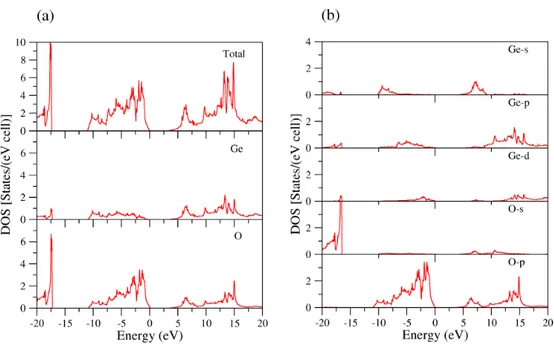
The research on silicon nitride has largely been driven by its use in microelec-tronics technology to utilize it as an effective insulating material and also as diffusion mask for impurities. Recently it started to attract attention both as a host embedding material for nanocrystals [47, 48, 49] and also for optical waveg-uide applications [40]. The α- and β-Si3N4 have hexagonal conventional cells with
four and two molecules, respectively. We used 60 Ha plane wave energy cutoff and 6×6×8 k-point sampling. The computed band structures of these two phases shown in Figs. 2.7 (a) and (b) are identical to those reported by Xu and Ching [67]. The top of the valence band for β-Si3N4 is along the Γ-A direction, and for
α-Si3N4 it is at the M point. The bottom of the conduction band for two phases
are at the Γ point. The direct and indirect LDA band gaps of these two phases are respectively, 4.559 eV, 4.621 eV for α-Si3N4 and 4.146 eV, 4.365 eV for the
β-Si3N4. The general band structure of two phases are very similar, except that
the α-Si3N4 has twice as many bands because the unit cell is twice as large. The
total DOS of these two phases shown in Figs. 2.7(a) and (b) are only marginally different. Calculated values of the elastic constants and bulk modulus of β-Si3N4
listed in Table 2.3 are in excellent agreement with the quoted experiments. Those
Figure 2.7: LDA band structure and total DOS of (a) α-Si3N4, (b) β-Si3N4, (c)
α-Ge3N4 and (d) β-Ge3N4.
for the α-Si3N4 which is thermodynamically less stable with respect to β-phase
[102] were left out due to excessive memory requirements for the desired accuracy. Ge3N4 is the least studied material among the oxides and nitrides considered
in this work. Recently its high-pressure γ-phase has attracted some theoretical interest [103]. However, the available Ge3N4 samples contain a mixture of α and
β-phases as in the case of Si3N4 and these are the polymorphs that we discuss in
this work. The band structures of both of these phases of Ge3N4 (cf. Fig. 2.7) are
theoretical results listed in Table 2.3 await experimental verification. In terms
Figure 2.8: Element-resolved DOS of (a) β-Si3N4; total, PDOS of Si, PDOS of
N, (b) β-Ge3N4; total, PDOS of Ge, PDOS of N.
of density, the β phases of Si3N4 and Ge3N4 fill the gap between the α-quartz
and stishovite/rutile phases of their oxides. As can be observed from Fig. 2.9
Figure 2.9: Density versus direction-averaged static electric susceptibility. their electric susceptibility versus density behavior strengthens the correlation established by the remaining polymorphs. Finally it can be noted that β-Ge3N4
has the largest high-frequency dielectric constant (ǫ∞) among all the materials
2.2
High-dielectric constant and wide band gap
inverse silver oxide phases of the ordered
ternary alloys of SiO
2, GeO
2and SnO
2High-dielectric constant and wide band gap oxides have important technological applications. The crystalline oxide polymorphs having lattice constant compat-ibility to silicon are particularly desirable. One recently reported candidate is the inverse silver oxide phase of SiO2. First-principles study of this system
to-gether with its isovalent equivalents GeO2, SnO2 as well as their ternary alloys are
performed. Within the framework of density functional theory both generalized gradient approximation (GGA) and local density approximation (LDA) are em-ployed to obtain their structural properties, elastic constants and the electronic band structures. To check the stability of these materials, phonon dispersion curves are computed which indicate that GeO2 and SnO2 have negative phonon
branches whereas their ternary alloys Si0.5Ge0.5O2, Si0.5Sn0.5O2, and Ge0.5Sn0.5O2
are all stable within LDA possessing dielectric constants ranging between 10 to 20. Furthermore, the lattice constant of Si0.5Ge0.5O2 is virtually identical to the
Si(100) surface. The GW band gaps of the stable materials are computed which restore the wide band gap values in addition to their high dielectric constants.
2.2.1
Introduction
High-dielectric constant and wide band gap oxides are of general interest for the next-generation gate oxides for silicon-based electronics [39] and also as host matrices for nonvolatile flash memory applications [104]. Amorphous oxides have been generally preferred as they are good glass-formers which tend to minimize the number of dangling bonds at the interface. In this respect, poly-crystalline oxides are undesirable as the grain boundaries cause higher leakage currents and possible diffusion paths for dopants [39]. On the other hand, crystalline oxide grown epitaxially on silicon [105] can be favorable as it will result in high interface quality provided that it is lattice-matched to Si.
Very recently, Ouyang and Ching [106] have reported a high-density cubic polymorph of SiO2 in the inverse Ag2O structure, named by them as the i-phase,
possessing both high dielectric constant, as in stishovite phase, and the lattice constant compatibility to Si(100) face which make it very attractive for electronic applications. In this part of the thesis, we report our contribution to this search for the crystalline high-dielectric constant oxides with the i-phases of GeO2 and
SnO2 as well as their ordered ternary alloys with SiO2. This pursuit is in line with
the International Technology Roadmap for Semiconductors where computational synthesis of novel high-dielectric materials is emphasized [107]. We employ the well-established ab initio framework based on the density functional theory within the GGA and LDA using pseudopotentials and a plane wave basis [108].
Figure 2.10: Ball and stick model of the i-phase ordered ternary alloy X0.5Y0.5O2.
2.2.2
Computational Details
The unit cell for the ordered ternary alloy X0.5Y0.5O2 in the inverse Ag2O
struc-ture is shown in Fig. 2.10. Structural and electronic properties of the i-phase structures under consideration have been calculated within the density functional theory [108], using the plane wave basis pseudopotential method as implemented in the ABINIT code [19]. The results are obtained under the the GGA and
LDA where for the exchange-correlation interactions we use the Teter-Pade pa-rameterization [73], which reproduces Perdew-Zunger [74] (which reproduces the quantum Monte Carlo electron gas data of Ceperley and Alder [75]).
We tested the LDA results under two different norm-conserving Troullier and Martins [76] type pseudopotentials, which were generated by A. Khein and D.C. Allan (KA) and Fritz Haber Institute (FHI); for either set, the d electrons were not included in the valence configuration. Our calculated values for these two types of pseudopotentials were very similar. In the course of both GGA and LDA computations, the plane wave energy cutoff and k-point sampling were chosen to assure a 0.001 eV energy convergence for all i-phase crystals. In the case of SiO2
this demands a 65 Ha plane wave energy cutoff and 10×10×10 k-point sampling. Phonon dispersions and phonon density of states were computed by the PHON program [109] using a 2 × 2 × 2 supercell of 48 atoms to construct the dynamical matrix1. The required forces were extracted from ABINIT. The corrected band
gap values are computed by obtaining self-energy corrections to the DFT Kohn-Sham eigenvalues in the GW approximation [110]. All parameters used during the GW calculation were chosen to assure a 0.001 eV energy convergence.
2.2.3
Results
Table 2.6: First-principles LDA and GGA structural data for i-phase crystals.
Crystal a (˚A) Density (gr/cm3 ) x-O (˚A) y-O (˚A) SiO2 LDA 3.734 3.830 1.617 GGA 3.801 3.633 1.646 GeO2 LDA 3.916 5.781 1.696 GGA 4.053 5.215 1.755 SnO2 LDA 4.180 6.864 1.808 GGA 4.452 5.671 1.928 Ge0.5Si0.5O2 LDA 3.836 4.843 1.697 1.625 GGA 3.923 4.528 1.762 1.635 Ge0.5Sn0.5O2 LDA 4.042 6.416 1.688 1.813 GGA 4.250 5.522 1.748 1.932 Sn0.5Si0.5O2 LDA 3.970 5.590 1.818 1.620 GGA 4.114 5.015 1.935 1.628
2.2.3.1 General
Using XO2 and X0.5Y0.5O2 as the generic notation, the O-X-O and O-Y-O bond
angles are 109.47◦ and the X-O-X and X-O-Y bond angles are 180◦ according to
the crystal construction of this cubic i-phase (cf. Fig. 2.10). Other structural information such as the lattice constants and bond lengths of all i-phase crystals are listed in Table 2.6. The Si(100) surface lattice constant is about 3.83 ˚A, therefore according to LDA results Si0.5Ge0.5O2 is of particular interest as it can
be epitaxially grown on Si without any strain. According to our well-converged calculations Si0.5Ge0.5O2 has a lower total energy compared to both SiO2 and
GeO2, the latter itself is unstable as will be shown later; this can be taken as
some indication of immunity to the phase separation of this ternary alloy into its binary compounds.
Table 2.7: Elastic constants and bulk modulus for each crystal.
Crystal C11(GPa) C12(GPa) C44(GPa) B(GPa)
SiO2 LDA 383.6 260.0 243.0 301 GGA 354.3 232.1 227.9 273 GeO2 LDA 297.0 231.2 175.6 253 SnO2 LDA 208.9 185.5 113.9 193 Ge0.5Si0.5O2 LDA 349.4 253.2 200.0 285 GGA 292.8 203.9 161.8 234 Ge0.5Sn0.5O2 LDA 255.4 210.8 106.3 226 Sn0.5Si0.5O2 LDA 277.5 217.4 103.9 237 GGA 238.3 183.0 202.8 201 2.2.3.2 Stability
The LDA and GGA results of the three independent elastic constants and bulk modulus for all crystals are tabulated in Table 2.7. An important concern is the stability of these cubic phases. The requirement of mechanical stability on the elastic constants in a cubic crystal leads to the following constraints: C11 > C12,
C11 > 0, C44 > 0, and C11+ 2C12 > 0. The elastic constants calculated by both
LDA and GGA shown in Table 2.7 satisfy these stability conditions. Furthermore, we compute the LDA and GGA phonon dispersion curves of these structures using the PHON program [109]. First, to verify the validity of the results of the PHON program we compute the phonon dispersions of the SiO2 and GeO2 by using both
Figure 2.11: LDA phonon dispersions of the unstable crystals: (a) GeO2, (b) SiO2.
PHON and ANADDB extension of the ABINIT code [19]. There exists a good agreement between two calculations. Next, we calculate the phonon dispersions of the all i-phase crystals via PHON program with forces obtained from LDA and GGA. It is observed that SiO2 is at least locally stable whereas GeO2 and SnO2
contains negative phonon branches which signal an instability of these phases (see Fig. 2.11). As for their alloy, Ge0.5Sn0.5O2, according to LDA this material is
stable whereas within GGA it comes out as unstable. For the stable structures the LDA phonon dispersions and the associated phonon DOS are shown in Fig. 2.12. Table 2.8: LDA and GGA dielectric permittivity tensor for the stable crystals.
Crystal ǫ0 xx= ǫ0yy=ǫ0zz ǫ ∞ xx= ǫ ∞ yy=ǫ ∞ zz SiO2 LDA 9.857 3.285 GGA 9.970 3.303 Ge0.5Si0.5O2 LDA 11.730 3.416 GGA 14.383 3.585 Ge0.5Sn0.5O2 LDA 19.415 3.527 Sn0.5Si0.5O2 LDA 12.883 3.360 GGA 18.096 3.711
For the stable systems, the static and high-frequency dielectric constants are listed in Table 2.8. The static dielectric constants falling in the range between 10 to 20 suggest that these are moderately high dielectric constant crystals. It can be observed that GGA yields systematically higher values for the dielectric constants of these structures. Employing KA pseudopotentials, the LDA band
Figure 2.12: LDA phonon dispersions and the phonon DOS (a. u.) of the stable crystals: (a) SiO2, (b) Ge0.5Si0.5O2, (c) Ge0.5Sn0.5O2, and (d) Si0.5Sn0.5O2.
structure for the crystals are displayed along the high-symmetry lines in Fig. 2.13 including the electronic DOS. The widths of the valence bands get progressively narrowed from Fig. 2.13(a) to (d), i.e., from SiO2 to Sn0.5Si0.5O2. For all of the
i-phase crystals under consideration including the unstable ones the conduction band minima occur at the Γ point whereas the valence band maxima are located at R point making them indirect band gap semiconductors. As tabulated in Table 2.9, the direct band gap values are only marginally above the indirect band gap values. Again GGA systematically yields narrower band gaps compared to LDA.
Figure 2.13: LDA electronic band structure and DOS (States/eV cell) of i-phase (a) SiO2, (b) Ge0.5Si0.5O2, (c) Ge0.5Sn0.5O2, and (d) Sn0.5Si0.5O2.
2.2.3.3 GW Band Gap Correction
A renown artifact of LDA is that for semiconductors and insulators band gaps are underestimated [108]. In this part of our work, the corrected band gap values are also provided by GW approximation. As there are different GW implementations we briefly highlight the particular methodology followed in the ABINIT code. First, a converged ground state calculation (at fixed lattice parameters and atomic positions) is done to get self-consistent density and potential, and Kohn-Sham
Table 2.9: Indirect (Eg) and direct (Eg,Γ) band gaps for each i-phase crystal
within LDA, GGA, and for the stable structures the GW approximation (GWA).
Crystal Eg (eV) Eg,Γ(eV)
SiO2 LDA 5.269 5.870 GGA 4.584 5.155 GWA 7.283 7.964 GeO2 LDA 2.402 2.511 SnO2 LDA 2.285 2.670 Ge0.5Si0.5O2 LDA 3.666 4.179 GGA 2.558 3.005 GWA 5.943 6.513 Ge0.5Sn0.5O2 LDA 2.487 2.900 GGA 0.767 0.865 GWA 4.533 4.972 Sn0.5Si0.5O2 LDA 3.292 3.900 GGA 1.763 2.304 GWA 5.484 6.153
eigenvalues and eigenfunctions at the relevant band extrema k-points as well as on a regular grid of k-points. Next, on the basis of these available Kohn-Sham data, the independent-particle susceptibility matrix χ0 is computed on a regular
grid of q-points, for at least two frequencies (usually, zero frequency and a large pure imaginary frequency - on the order of the plasmon frequency, a dozen of eV). Finally, the Random Phase Approximation susceptibility matrix, χ, the dielectric matrix ǫ and its inverse ǫ−1 are computed. On this basis, the
self-energy, Σ matrix element at the given k-point is computed to derive the GW eigenvalues for the target states at this k-point. Note that this GW correction is achieved as a one-shot calculation (i.e., no overall self-consistency) hence, our results technically corresponds to G0W0 which has been the standard approach
as originally proposal by Hedin [111]. The GW correction as can be observed from Table 2.9 restores the wide band gap values; this feature is essential for these materials to provide sufficient confinement to carriers of the narrow band gap semiconductors such as silicon.
2.2.3.4 Final Remarks
We have also considered the i-phase of PbO2 which turned out to be unstable and
hence its ab initio data are not included. In this work, we do not consider the thermodynamic stability of these i-phase oxides. However, for technological ap-plications rather than bulk systems the epitaxial growth conditions become more
critical [112]. A promising direction can be the finite temperature investigation [113] of these i-phase isovalent structures on Si(100) surfaces using large number of monolayers.
Modeling of the Hot Carrier
Transport Through SiO
2
and the
Quantum-Confined Impact
Ionization Processes
Injected carriers from the contacts to delocalized bulk states of the oxide ma-trix via Fowler-Nordheim tunneling can give rise to quantum-confined impact ionization (QCII) of the nanocrystal (NC) valence electrons. This process is re-sponsible for the creation of confined excitons in NCs, which is a key luminescence mechanism. For a realistic modeling of QCII in Si NCs, a number of tools are combined: ensemble Monte Carlo (EMC) charge transport, ab initio modeling for oxide matrix, pseudopotential NC electronic states together with the closed-form analytical expression for the Coulomb matrix element of the QCII. To character-ize the transport properties of the embedding amorphous SiO2, ab initio band
structure and density of states of the α-quartz phase of SiO2 are employed. The
confined states of the Si NC are obtained by solving the atomistic pseudopoten-tial Hamiltonian. With these ingredients, realistic modeling of the QCII process involving a SiO2 bulk state hot carrier and the NC valence electrons is provided.
3.1
Introduction
Due to its indirect band gap, bulk Si is a very inefficient emitter, even at liq-uid He temperatures. Within the last decade, several approaches were developed towards improving the efficiency of light emission from Si-based structures. In spirit, all were based on the lifting of the lattice periodicity that introduces an uncertainty in the k-space and therefore altering the indirect nature of this ma-terial. Some examples are: SiGe or Si\SiO2 superlattices [1, 2] or Si nanocrystal
(NC) assemblies [3]. Recently, blue electroluminescence (EL) from Si-implanted SiO2 layers and violet EL from Ge-implanted SiO2 layers were observed. An
im-portant process responsible for EL occurring in quantum dots and NCs is the quantum-confined impact ionization (QCII). A carrier initially at a high energy
Figure 3.1: Quantum-confined impact ionization in NCs.
electron of a NC across its band gap creates an electron-hole pair (cf. Fig. 3.1). This process is responsible for the introduction of confined excitons in silicon NC LEDs, which is a key luminescence mechanism. In contrast to its crucial role, QCII has not been given the attention it deserves.
To model the QCII process, we start by characterizing the hot electron trans-port in oxides within the ensemble Monte Carlo (EMC) framework. Our EMC code [114, 115] includes all major scattering mechanism such as acoustic, polar and non-polar optical phonon scatterings. Density of states and band structure of common crystal phases of the SiO2 used in our Monte Carlo transport
calcula-tion were described in Chapter 2 of this thesis. As the main contribucalcula-tion of this part of the thesis, we derive an analytical expression for the QCII probability in NCs that can become an instrumental result in assessing EL in the presence of other competing scattering mechanisms. The effect of QCII on bulk transport quantities is also discussed.
3.1.1
Theoretical Details
Details about first principles calculations can be found in Chapter 2. Here, we demonstrate the utility and the validity of our ab initio DOS results by studying the high-field carrier transport in bulk SiO2 up to fields of 10 MV/cm using the
EMC technique. The corresponding scattering rates are intimately related with the band structure and the DOS of SiO2 for which we use those of the α-quartz
phase due to its strong resemblance of the amorphous SiO2 in terms of both the
short-range order and the total DOS [116]. Aiming for very high fields around 10 MV/cm, we also include the impact ionization process within the bulk SiO2
medium; the relevant parameters were taken from the work of Arnold et al. [117]. Our modeling for QCII is an extension of the approach by Kehrer et al. who have dealt with the high-field impurity breakdown in n-GaAs [118]. We assume the impacting carrier to be an electron, however all of the formulation can be reiterated by starting with an impacting high energy hole in SiO2. Above the