sensors
ISSN 1424-8220www.mdpi.com/journal/sensors Article
Circular High-Q Resonating Isotropic Strain Sensors with Large
Shift of Resonance Frequency under Stress
Rohat Melik 1,2, Emre Unal 2, Nihan Kosku Perkgoz 2, Christian Puttlitz 4 and Hilmi Volkan Demir 1,2,3,*
1
Department of Electrical and Electronics Engineering, Bilkent University, Bilkent, 06800 Ankara, Turkey; E-Mail: [email protected]
2
Nanotechnology Research Center, and Institute of Materials Science and Nanotechnology, Bilkent University, Bilkent, 06800 Ankara, Turkey; E-Mails: [email protected] (E.U.);
[email protected] (N.K.P.)
3
Department of Physics, Bilkent University, Bilkent, 06800 Ankara, Turkey
4
Department of Mechanical Engineering and School of Biomedical Engineering, Orthopaedic Bioengineering Research Laboratory, Colorado State University, Fort Collins, CO 80523, USA; E-Mail: [email protected]
* Author to whom correspondence should be addressed; E-Mail: [email protected]; Tel.: +90(312)2901012; Fax: +90(312)2901015.
Received: 31 August 2009; in revised form: 13 October 2009 / Accepted: 3 November 2009 / Published: 25 November 2009
Abstract: We present circular architecture bioimplant strain sensors that facilitate a strong
resonance frequency shift with mechanical deformation. The clinical application area of these sensors is for in vivo assessment of bone fractures. Using a rectangular geometry, we obtain a resonance shift of 330 MHz for a single device and 170 MHz for its triplet configuration (with three side-by-side resonators on chip) under an applied load of 3,920 N. Using the same device parameters with a circular isotropic architecture, we achieve a resonance frequency shift of 500 MHz for the single device and 260 MHz for its triplet configuration, demonstrating substantially increased sensitivity.
Keywords: RFIC; Q-factor; resonators; circular architecture; bioMEMS sensors; frequency
shift; sensitivity
1. Introduction
Fixation plates are routinely used for major bone fracture cases. As the healing tissue develops stiffness and strength, the load borne by the plate decreases [1]. During this process, a sensor capable of monitoring strain telemetrically and in real time is highly desirable. When force is applied to the sensor via its attachment to the fixation plate, the resulting strain is observed via a resonance frequency (fo)
shift. Using this emerging technology, physicians would be able to assess the healing process by examining these temporal changes in strain.
Previously, we developed high quality factor (Q-factor) on-chip resonators [2] and demonstrated the proof-of-concept for utilizing the resonance frequency shift as an indirect measure of strain [3]. In this work, we significantly increased the sensor Q-factor and resonance frequency shift compared to the architectures used in the previous works. Here we present a circular architecture RF-MEMS bioimplantable strain sensor that demonstrates a substantially higher Q-factor and larger frequency shift compared to a rectangular architecture.
2. Design and Fabrication
For our resonators, we aim for a high Q-factor by using bio-compatible materials with a maximum possible resonance frequency shift. To design the resonator in a distributed spiral coil architecture with a high Q-factor (Figure 1), we consider the effects of substrate, dielectric material, dielectric thickness (tfilm), metal material, metal layer thickness (tmetal), metal width (w) and spacing (s), number of turns (N),
and area (Wc x Lc) as explained in [2]. Further details of the formulas and techniques for Q-factor
enhancement can be found in [4-13]. For biocompatibility, we choose to use silicon as the substrate, gold as the metal layer, and SixNy as the dielectric layer. Our main design strategy in achieving a
maximum Q-factor with minimum spacing relies on the use of the distributed film capacitance as the LC tank circuit capacitance. The dominant parameter driving the resonance frequency shift is the on-chip capacitance change with mechanical deformation, allowing for strain measurement from the sensor without requiring additional circuitry. Although strain sensors using digital electronics [14,15] have been reported in the archival literature, the current work, to the best of our knowledge, represents the first account of an RF-based MEMS strain sensor in different architectures (circular geometries).
The following details using a circular architecture that better optimizes the aforementioned design aims. We compare two sensors with the same design parameters in rectangular and circular geometries shown in Figure 1. In both cases, the total size (Wc × Lc) is 340 µm × 340 µm. In addition, both
architectures have 2 turns (N), 60 µm wide metal width (w) and 10 µm wide spacing between coil segments (s). Their metal film thickness (tmetal) is 0.1 µm while their dielectric film thickness (tfilm) is
also 0.1 µm. The circular architecture has an effectively reduced total area compared to the rectangular geometry with the same dimensions. Thus, for the circular architecture, we obtain smaller film capacitance and coil inductance, yielding a higher fo. Also, we have lower coil resistance, lower loss,
higher substrate resistance, and lower substrate capacitance. This produces a higher substrate loss factor and self-resonance factor, which is discussed in detail in [2]. As a result, with smaller spacing and higher fo in the circular geometry, we achieve a higher inductor Qind-factor (and thus a higher resonator
Figure 1. (a) Top-view single rectangular device, (b) top-view single circular device, (c)
cross-sectional view of the device (d) top-view rectangular triplet configuration,
(e) top-view circular triplet configuration, and (f) schematic illustration of the externally
applied load.
We approach the increase in the resonance frequency shift from two perspectives. First, the deformation is equally effective in any direction, thanks to the isotropic geometry as depicted in Figure 2a. On the contrary, in a rectangular geometry, there is a preferential, anisotropic deformation, which dominates unilaterally (effective on only one side at a time) as illustrated in Figure 2b. In Figure 2, we can see that the maximum deformation of circular and rectangular shapes are the same but in rectangular geometry, one side is not deformed while in circular geometry, the whole geometry deformation is nearly the same. Therefore, the capacitance change in the circular case is higher than that in the rectangular case with the same starting initial capacitance value because the deformation acts to change the whole geometry. Hence, the associated resonance frequency shift is expected to be larger. Next, even if we have the same frequency shift ratio, Δfo/fo (relative shift), the frequency shift is higher
in the circular geometry since it possesses a higher fo. If we combine these two aspects, we have much
higher shift for the circular case. Therefore, using the circular architecture, we expect to obtain a higher Δfo and a higher sensitivity, e.g., defined as fo F (or asfo ) with respect to the applied load (F)
[or the induced strain (ɛ )]. Simulating S21 parameters for the rectangular and circular devices and their
triplet configurations, we also obtain higher resonance frequencies and higher Q-factors for the circular geometry. Thus, we predict better performance with the circular architecture.
Figure 2. Coventorware simulations of the strain distribution of the deformed devices when
a load of 1,960 N is applied from the bottom (a) in a circular geometry and (b) in a rectangular geometry. The z-direction is scaled down by a factor of 10 for a better view of the image.
(a)
(b)
For the implementation of our devices, our fabrication process begins with deposition and patterning of a 0.1 μm thick metal contact layer (Au) on the substrate (Si), and subsequent deposition of a 0.1 μm thick dielectric layer (SixNy), a cross-sectional view of which is shown in Figure 1c. We obtained the
specific patterning with lithography and wet etching by hydrofluoric acid (HF). Subsequently, we metalized the open parts with 0.1 μm thick Au layer. Finally, another 0.1 μm thick final metal layer (Au) is deposited on top. The fabricated devices can be seen in Figures 1a,b,d,e.
3. Experimental Characterization and Analysis
To characterize our fabricated devices, we apply a point load to our devices in a controllable manner using the same method as in [3], where its schematic illustration is given in Figure 1f, and measure the device S21 parameter in response to the applied load. Thus, the change in resonance frequency and the
Q-factor due to the applied load are determined. Our experimental set up includes an adjustable ultrafine-screw that can be adjusted to push towards the backside of the sensor. When the tip of this
screw just touches the sensor backside, no load is applied, as verified by our reference strain gauge (made by Kyowa, Japan, with a gauge factor of 178). The screw is further twisted to apply load and induce strain. We confirmed the levels of strain induced with the position of the ultrafine-screw using our reference strain gauge.
For bioimplant sensing applications, there is an absolute requirement to measure and report strain remotely in the absence of wiring. Thus, for the current and future evaluations of this technology we need to measure and compare the telemetric performance of these sensors. To this end, we configure three resonators side by side on the same chip (in triplet configuration) and obtain an on-chip telemetry system. Although this on-chip system does not fully comply with the actual clinical application, it provides a robust methodology to compare different devices with respect to their telemetric operation. In this triplet configuration, the middle device serves as the sensor, with the lateral devices serving as the transmitter and receiver antennas. For calibration purposes, we measure the S21 parameter of the
case where there are only transmitter and receiver antennas, and then measure the S21 parameters of our
triplet configuration to obtain the resonance frequency and Q-factor. When the load is applied to the chip, the calibrations are again repeated with the same procedure as explained above to observe the changes in the resonance frequency and Q-factor. Also, using identical antennas guarantee to see the resonance frequency of the sensor since the working band of the antenna will definitely catch the resonance frequency of the sensor. Since the triplet method is used for easy coupling, using the antennas identical to the sensor makes our measurements further easier. A more detailed description of the triplet configuration operating principles is given in [3].
The human body presents a more complex environment compared to the lab environment. This side-by-side testing scenario (in triplet configuration) is an idealized one, as this configuration provides merely an in vitro characterization platform. Having characterized the operation of these sensors in a side-by-side configuration, our future research work will include performing animal model experiments. We anticipate that there will be differences in the performance of our sensor when placed in the in vivo environment. Specifically, we expect reduced sensitivity levels due to the complex nature of the in vivo measurement medium. We also expect that the circular architecture will greatly enhance some of the proposed application areas for this sensor due to the significantly improved sensing performance of the circular designs.
Figures 3a through 3d present S21 (in dB) as a function of operating frequency for the single
rectangular, single circular, triplet rectangular, and triplet circular configurations, respectively. All of these figures also include a zoom-in view (in the inset) of the data around the resonance frequencies.
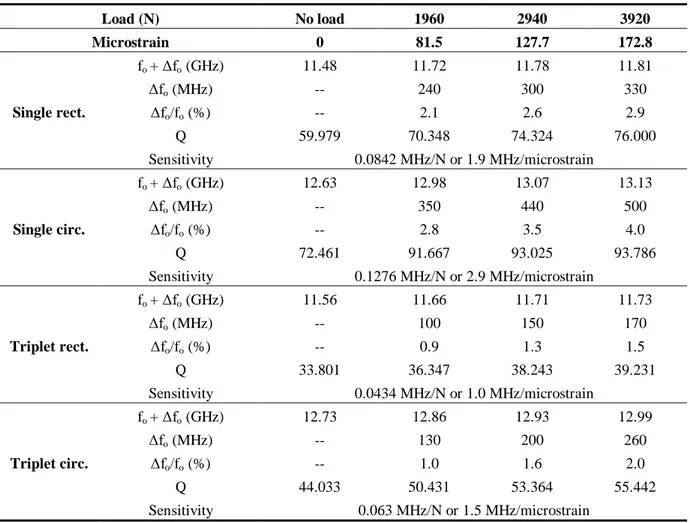
Table 1 lists the measured resonance frequencies in response to the applied loading, clearly showing that the resonance frequency increases with the applied force due to decreasing area, and hence, decreasing capacitance. Also, all of these experimental S21 data measured under zero external load are in
agreement with our numerical simulations (in CST Microwave Studio).
In Table 1, we also present the resonance frequency changes. The resulting resonance frequency increase is higher for all of the circular device geometries as explained above. Since the area decrease is not linear and the capacitance is not linearly proportional to the resonance frequency, the resulting frequency increase is expectedly nonlinear. In addition, since the frequency shift is much higher in the circular cases compared to the rectangular cases, we observe higher relative shift and higher sensitivity for the circular cases in Table 1.
Figure 3. Experimental measurements of S21 parameters (dB) as a function of operating
frequency (GHz) for (a) the single rectangular device, (b) the single circular device, (c) the rectangular triplet configuration, and (d) the circular triplet configuration under the applied loads of 1,960 N, 2,940 N, and 3,920 N, along with their zoom-in S21 parameters (dB) vs.
operating frequency (GHz) (where the numbers of inset axes are grey colored) given around their resonances in the insets.
Table 1. Resonance frequencies, resonance frequency shifts, relative shifts, Q-factors, and
sensitivities of our devices given as a function of changing load and induced strain levels.
Load (N) No load 1960 2940 3920 Microstrain 0 81.5 127.7 172.8 Single rect. fo + Δfo (GHz) 11.48 11.72 11.78 11.81 Δfo (MHz) -- 240 300 330 Δfo/fo (%) -- 2.1 2.6 2.9 Q 59.979 70.348 74.324 76.000 Sensitivity 0.0842 MHz/N or 1.9 MHz/microstrain Single circ. fo + Δfo (GHz) 12.63 12.98 13.07 13.13 Δfo (MHz) -- 350 440 500 Δfo/fo (%) -- 2.8 3.5 4.0 Q 72.461 91.667 93.025 93.786 Sensitivity 0.1276 MHz/N or 2.9 MHz/microstrain Triplet rect. fo + Δfo (GHz) 11.56 11.66 11.71 11.73 Δfo (MHz) -- 100 150 170 Δfo/fo (%) -- 0.9 1.3 1.5 Q 33.801 36.347 38.243 39.231 Sensitivity 0.0434 MHz/N or 1.0 MHz/microstrain Triplet circ. fo + Δfo (GHz) 12.73 12.86 12.93 12.99 Δfo (MHz) -- 130 200 260 Δfo/fo (%) -- 1.0 1.6 2.0 Q 44.033 50.431 53.364 55.442 Sensitivity 0.063 MHz/N or 1.5 MHz/microstrain
Table 1 also provides Q-factor data, which are observed to be high despite the relatively small chip sizes. These Q-factors are particularly higher in the circular case with a smaller area. The Q-factor is increased as the load magnitude is increased due to a lower Cfilm, as discussed in [2] and [3]. The
Q-factor also increases for the telemetric case of the circular case compared to the rectangular case. However, in the telemetric operation, due to coupling between resonators, the signal is decreased and Q-factors are reduced for both of the rectangular and circular cases compared to the single device cases. Our experimental apparatus can reproducibly apply a minimum strain of 81.5 microstrain, while the maximum strain is 172.8 microstrain. Therefore, it is not possible to make a direct measurement of the minimum detectable strain level for our sensors. Since the resolution of the network analyzer that we use in our experiments is 1 Hz (given the typical noise level in our experiments), we find the resolution of our sensors in the strain range across which they are tested by dividing this minimum detectable frequency to their sensitivities. From this calculation, we obtain 526.3 femtostrain for single rectangular device and 344.8 femtostrain for single circular device. These resolutions are better than those reported in [15].
Another interesting point for discussion is the hysteresis behavior. When different levels of external load are successively applied without allowing the mechanical setup to fully relax into the new loading conditions (typically in a time scale of minutes), we observe a memory effect and see a hysteresis in the experimental characterization of these sensors. The sensors in circular geometry exhibit a wider hysteresis loop as expected because they are more sensitive sensors, compared to those in the rectangular geometry. However, if one waits long enough (minutes) between successive force levels, no hysteresis is observed. The experimental data presented here is for the case of no hysteresis.
4. Conclusions
In summary, we have designed, fabricated, and experimentally characterized isotropic circular strain sensor resonators that allow for higher Q-factors with smaller spacing compared to rectangular designs. The circular architecture enables a significantly higher resonance frequency shift and sensitivity (both with respect to applied force and induced strain) because of its isotropic geometry. This results in a substantial improvement in the performance of these resonators for use as bioimplant strain sensors. With their promising properties and biocompatibility, our sensors are currently being investigated for the assessment of osseous fractures through monitoring the shift in the resonance frequency in response to the acting load.
Acknowledgements
We acknowledge Z. Dilli for valuable discussions.
References and Notes
1. Stoffel, K.; Klaue, K.; Perren, S.M. Functional load of plates in fracture fixation in vivo and its correlate in bone healing. Injury 2000, 31, 37–50.
2. Melik, R.; Perkgoz, N.K.; Unal. E.; Dilli, Z.; Demir, H.V. Design and realization of a fully on-chip high-Q resonator working at 15 GHz on silicon. IEEE Trans. Electron Devices 2008, 55, 3459–3466.
3. Melik, R.; Perkgoz, N.K.; Unal. E.; Puttlitz, C.; Demir H.V. Bio-implantable passive on-chip RF-MEMS strain sensing resonators for orthopaedic applications. J. Micromech. Microeng. 2008, 18, No.115017.
4. Yue, C.P.; Wong S.S. On-chip spiral inductors with patterned ground shields for Si-based RF IC’s. IEEE J. Solid-State Circuits 1998, 33, 743–752.
5. Yue, C.P.; Ryu, C.; Lau, J.; Lee, T.H.; Wong, S.S. A physical model for planar spiral inductors on silicon. In Proceedings of the IEEE International Electron Devices Meeting, San Francisco, CA, USA, December 8–11, 1996; pp. 155–158.
6. Greenhouse, H.M. Design of planar rectangular microelectronic inductors. IEEE Trans. Parts, Hybr. Packag. 1974, 10, 101–109.
7. Koutsoyannopoulos, Y.K.; Papananos, Y. Systematic analytic and modeling of integrated inductors and transformers in RFIC design. IEEE Trans. Circuits Syst. 2000, 47, 699–713.
8. Zolfaghari, A.; Chan, A.; Razavi, B. Stacked inductors and transformers in CMOS technology. IEEE J. Solid-State Circuits 2001, 36, 620–628.
9. Long J.R.; Copeland M.A. The modeling, characterization, and design of monolithic inductors for silicon RF IC’s. IEEE J. Solid-State Circuits 1997, 32, 357–369.
10. Bahl, I. Lumped Elements for RF and Microwave Circuits; Artech House: London, UK, 2003; pp. 57–118.
11. Collin, R.E. Foundations for Microwave Engineering; McGraw Hill: New York, NY, USA, 1992; pp. 71–96.
12. Pozar, D.M. Microwave Engineerin; J. Wiley & Sons: New York, NY, USA, 2005; pp. 49–64. 13. Lee, T.H. The Design of CMOS Radio-Frequency Integrated Circuits; Cambridge University Press:
New York, NY, USA, 1998; pp. 47–57.
14. Suster, M.; Guo, J.; Chaimanonart, N.; Ko, W.H.; Young, D.J. Low-noise CMOS integrated sensing electronics for capacitive MEMS strain sensors. In Proceedings of the IEEE 2004 Custom Integrated Circuits Conference, Orlando, FL, USA, October, 2004; pp. 693–696.
15. Wojciechowski, K.E.; Boser, B.E.; Pisano A.P. A MEMS resonant strain sensor with 33 nano-strain resolution in a 10 kHz bandwidth. In Proceedings of 2005 IEEE Sensors, Irvine, CA, USA, October 30–November 3, 2005; pp. 947–950.
© 2009 by the authors; licensee Molecular Diversity Preservation International, Basel, Switzerland. This article is an open-access article distributed under the terms and conditions of the Creative Commons Attribution license (http://creativecommons.org/licenses/by/3.0/).