PROCEEDINGS OF SPIE
SPIEDigitalLibrary.org/conference-proceedings-of-spie
High quantum efficiency Type-II
superlattice N-structure
photodetectors with thin intrinsic
layers
Yuksel Ergun
Mustafa Hostut
Tunay Tansel
Abdullah Muti
Abidin Kilic
Rasit Turan
Atilla Aydinli
High quantum efficiency Type-II superlattice N-structure
photodetectors with thin intrinsic layers
Yuksel Erguna*, Mustafa Hostutb, Tunay Tanselc, Abdullah Mutid, Abidin Kilica, Rasit Turanc, Atilla Aydinlid
a Department of Physics, Anadolu University, 26470 Eskisehir, Turkey b
Department of Second. Edu. Sci. & Maths, Akdeniz University, 07058 Antalya, Turkey
c
Department of Physics, Middle East Technical University, 06531 Ankara, Turkey
d Department of Physics, Bilkent University, 06800 Ankara, Turkey
ABSTRACT
We report on the development of InAs/AlSb/GaSb based N-structure superlattice pin photodiode. In this new design, AlSb layer in between InAs and GaSb layers acts as an electron barrier that pushes electron and hole wave functions towards the GaSb/InAs interface to perform strong overlap under reverse bias. Experimental results show that, with only 20 periods of intrinsic layers, dark current density and dynamic resistance at -50 mV bias are measured as 6x10⁻³ A/cm2 and 148 Ωcm2 at 77K, respectively. Under zero bias, high spectral response of 1.2A/W is obtained at 5 μm with 50% cut-off wavelengths (λc) of 6 μm. With this new design, devices with only 146 nm thick
i-regions exhibit a quantum efficiency of 42% at 3 μm with front-side illimunation and no anti-reflection coatings.
Keywords: N-structure InAs/AlSb/GaSb superlattice pin photodiode, Mid-Wave-Infrared Photodiode, cut-off
wavelengths, spectral response of InAs/GaSb,
1. INTRODUCTION
Regarding the promising 6.1 Å material family, flexible combination of InAs/AlSb/GaSb superlattice layers allow the design of high performance type-II superlattice (T2SL) detectors having high quantum efficiency and high detectivity since their band structures can be modified with minimized Auger recombination rate, high carrier effective mass and strong carriers overlap [1]. There have been some high performance and high quality T2SL infrared detector structures given in the literature up until now. These include either single color [2] or dual-color [3] InAs/GaSb SL based pin photodiodes and heterojunction detector designs. The heterojunction detectors may be
Infrared Technology and Applications XXXIX, edited by Bjørn F. Andresen, Gabor F. Fulop, Charles M. Hanson, Paul R. Norton, Proc. of SPIE Vol. 8704, 870414 · © 2013 SPIE
CCC code: 0277-786X/13/$18 · doi: 10.1117/12.2016133 Proc. of SPIE Vol. 8704 870414-1
classified in two categories. The first category includes minority carrier unipolar detectors where the photogenerated minority carriers contribute to transport, while majority carriers are blocked by the barrier, such as the case in nBn [4-6], pBp [7], pMp [8] and bulk XBn [9] detectors. The second cathegory includes double heterojuction designs such as, W-structure [10], graded bandgap WSL (GGW) photodiodes [11], M-structure (p-π-M-n) [12], CBIRD [13], PbIbN [14], DBBD structures[15] and ICIP[16]. Their performans levels have been improved by increasing the quantum efficiency, detectivity and dynamic resistance area product (R0A) and reducing the dark current. Quantum
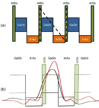
efficiencies of XBn detectors [17] as bulk structures and on type-II superlattices [18] have reached up to 70%. Recently, we have proposed an alternative design of InAs/AlSb/GaSb based T2SL pin fotodiode where InAs/GaSb SL layers are confined by AlSb layers [19]. Band structures have also been investigated for performance characteristics as well as heavy-hole light-hole (hh-lh) splitting, band gap and bonding properties [20]. All the layers of this p-i-n design have the same growth conditions as the standard T2SL p-i-n diodes such as layer thicknesses and layer sequences to avoid practical growth diffuculties seen in heterojunction designs. The structure is called the N-structure for resembling the letter N- of the band alignment of the AlSb/GaSb/InAs/AlSb layers as shown in Figure 1(a). Insertion of AlSb layers act as blocking barriers which play an important role for enhancing carrier overlap at GaSb/InAs interfaces by shifting the hole- wave functions towards GaSb/InAs interfaces. With this design 25% higher overlap is obtained at GaSb/InAs interfaces compared to standard InAs/GaSb T2SL pin diodes (Figure 1 (b)). In our experiments, detectivity of N-structure design is obtained to be ~1014 Jones at 77K and at zero bias. Electrical data show that RA and dark current density are measured as 3.7×10⁵Ωcm2 and 5.3×10⁻⁷A/cm2 under operating bias of -0.3V and 77K.
(a)
AISb AISb AISb AISb
Figure 1. (a) Conduction and valance band profiles for the proposed InAs/AlSb/GaSb based T2SL “N” structure. (b) Overlap integral for InAs/AlSb/GaSb based N-structure with AlSb barrier (red line) and Standard InAs/GaSb T2SL without AlSb barrier (black line) under 0.001meV bias. Negative bias is applied to the right side of the structure.
In this letter, we report on the electrical and optical properties of the new short period InAs/AlSb/GaSb based type-II N structure design with different constituent layer thicknesses. The optical results on responsivity and quantum efficiency measurements are impressive for photovoltaic mode applications.
2. EXPERIMENTAL
The superlattice photodiode was grown by commercially (IQE Inc. USA) with molecular beam epitaxy on a GaSb substrate. First a 100 nm GaSb buffer layer is deposited on unintentionally p-type doped (100) GaSb substrate followed by a 20nm lattice matched Al0,5Ga0,5As0,04Sb0,96 buffer layer. 300nm thick n-type InAs0.89Sb0.11:Te
(n=5×10¹⁷
cm-3) bottom contact is grown on the buffer layer. The p-i-n detector structure consists of 1/14.5/2/6.5 monolayers (MLs) of InSb/InAs/AlSb/GaSb SL layers as 20 periods of n-region with InAs:Te (5×1017 cm-3), 20 periods of i-intrinsic region and 30 periods of p-region with GaSb:Be (5×1017cm-3) respectively. The device was terminated by 45 nm GaSb:Be doped p-contact (8×1017 cm-3). The schematic view of layer configuration for the N-structure is given in Figure 2.
Proc. of SPIE Vol. 8704 870414-3
Top Contad GaSb:Be 8x1017cm3
p- InAs /AISb /GaSb SL 30 Per. i -InAs /AISb /GaSb SL 20 Per. n- InAs /AISb /GaSb SL 20 Per. Bottom Contact InAsSb:Te 5x1017cm3
Al Ga As
Sb buffer layer0,5 0,5 0,04 0,96
GaSb Substrate
Figure 2. Schematic view of InAs/AlSb/GaSb based SL N-Structure on GaSb substrate.
High resolution x-ray diffraction (HRXRD) spectrum of the grown wafer is shown in Figure 3. The periodicity of the superlattice as well as the mismatch of the zeroth order superlattice diffraction peak to the underlying GaSb substrate were determined using symmetric (004) X-Ray diffraction peak. Narrow FWHM of the peaks and higher order diffraction represents perfect crystalline quality and uniform superlattice periods at the grown epilayer.
2331608Ex20'
16-(-2) 1d-(-3) 10, -10° l,+,L
28.0 28.5 29.0 SL O GaSbGaSb /InAs Rev4 Short
( +2) ( +3) 30.0 30.5 31.0 31.5 Omegal2Theta (deg) N 0
Figure 3. High resolution x-ray diffraction curves of the superlattice along the 004 direction. Narrow FWHM of the peaks and highly ordered diffraction indicates uniform SL periods through the grown epilayer and excellent crystalline quality
A linear least squares fit of the peak spacing was used to determine the periodicity of the structure as 76.9Å. The mismatch between the SL and the GaSb substrate is determined as only 672 ppm, which is lower than the zero lattice mismatch limit (<1000 ppm). Single pixel photodetectors were fabricated with mesa sizes of 400×400 and 500×500 µm2
. To minimize surface damage, mesas have been fabricated by standard lithography and phosphoric acid based wet etch solution. The etch process was stopped when etch depth reached the bottom contact layer. A protective 300 nm thick SiO2 layer has been deposited using plasma enhanced chemical vapor deposition (PECVD) system at 250
C0 with %2SiH4/N2 and N2O gas flows of 180 sccm and 250 sccm, respectively. Ohmic contacts were made by
evaporating 5 nm Titanium (Ti) and 200 nm Gold (Au) on the bottom and top contact layers of the detectors. Sample was bonded to a chip carrier for further characterization. Electrical performance of the “N” design superlattice barrier structure have been investigated by using a HP4142OA source-measure unit. Samples were mounted on a nitrogen cooled closed cycle cold finger with a cold shield system. Dark current measurements were performed at 77K. The responsivity of the detector has been measured using calibrated blackbody source at 450 0C (Newport, Oriel 67000), lock-in amplifier (SRS, SR830 DSP) and mechanical chopper (SRS, SR540) system.
3. RESULT AND DISCUSSION
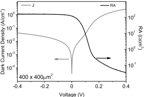
Figure 4 shows the voltage dependence of dark current density and RA at 77K. The dark current density is measured as 6x10⁻³ A/cm2 and corresponding RA is determined as 148 Ωcm2 under -50 mV bias voltage.
Proc. of SPIE Vol. 8704 870414-5
Figure 4. Dark current density and RA-voltage characteristics for SiO2 passivated sample at 77K.
RA product stays constant from 0 to -0.4V bias range indicating that the structure is for stable FPA operation. Under zero bias, dark current density was measured as low as 3.7x10⁻⁵ A/cm2 at 77K. Figure 5shows the spectral response of N-structure at 79K.
Figure 5. Spectral response of N-structure for SiO2 passivated and unpassivated samples at 79K.
-0.4
-0.2
0
0.2
0.4
10
-410
-310
-210
-110
0D
a
rk
C
u
rr
e
n
t
D
e
n
sit
y
(A
/c
m
2)
Voltage (V)
J400 x 400
m
210
-110
010
110
2 RAR
A
(
cm
2)
3
4
5
6
7
0.2
0.4
0.6
0.8
1.0
1.2
SiO2 passivated unpassivatedRes
p
o
n
siv
ity
(
A
/W)
Wavelenght (
m)
c= 6
m
400x400
79K
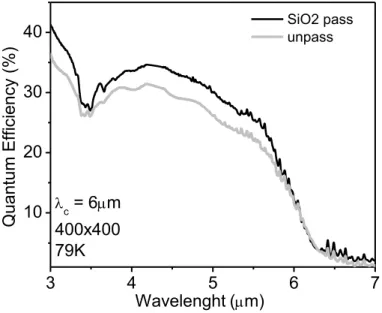
Responsivity spectra are obtained as high as 1.23 and 1.1 A/W at 5 μm with 50% cut-off wavelengths of 6 μm for both passivated and unpassivated samples, respectively. Responsivity spectra show that the confinement of the carriers at the GaSb interfaces are increased due to AlSb barriers under reverse bias, leading to strong overlap and type-II transitions. Quantum efficiency (QE) was calculated for single pass front illimunation conditions in the photovoltaic mode. Figure 6 shows the spectral dependence of QE for SiO2 passivated and unpassivated samples.
Figure 6. Quantum efficiency of N-Structure for SiO2 passivated and unpassivated samples at 79K.
The detector structure exhibits 100% cut-off wavelength of 7 μm and 50% cut-off at 6 μm at 79K. The QEs reach the peak values of 42% and 37% at 5 μm for passivated and unpassivated samples, respectively. Moreover, it shows that SiO2 passivation increases the responsivity as well as the quantum- efficiency values, which is attributed to the
effective suppression of surface leakage currents [21,22]. These values are impressive for a short period superlattice with only 146 nm thick i-region with a single-pass and no antireflection coating.
The QE revealing photovoltaic mode allows for the device operation at small reverse bias with a low dark current. In other words, photogenerated carriers contributed to photocurrent have long diffusion lengths that reach the electrodes withought the need for any additional electric field. Johnson-noise limited detectivity (D*) is determined from the quantum efficiency masurement and under zero bias, the peak D* is calculated as 5.5×10¹¹ Jones at 5 μm and 77K.
3
4
5
6
7
10
20
30
40
SiO2 pass unpassQ
uan
tum
E
ffi
ci
ency
(%
)
Wavelenght
(
m)
c= 6
m
400x400
79K
Proc. of SPIE Vol. 8704 870414-7
CONCLUSION
We have shown that high optical performance is possible for InAs/AlSb/GaSb based type-II SL N structure pin photodiode with very thin intrinsic layers. AlSb barriers in the structure push carriers towards InAs/GaSb interfaces that lead to strong electron and hole wavefunction overlap leading to high responsivity and quantum efficiency. The peak responsivity was measured as 1.23 A/W at 5 μm with 50% cut-off wavelengths (λc) of 6 μm. Corresponding QE
at 5 μm was about 30% for single pass into the 146nm thick i-region with front-side illimunation and no anti-reflection coatings. Under zero bias, the peak D* was calculated as 5.5×10¹¹ Jones at 5 μm and 77K.
ACKNOWLEDGMENTS
Y. Ergun acknowledges the support of TUBITAK and Anadolu University (Grants from Tubitak: 109T072 and BAP: 1104F073-1104F074 respectively). M. Hostut also acknowledges the support of Akdeniz University (BAP Grant: 2012.01.0110.002 ).
REFERENCES
[1] A. M. Hoang, G. Chen, A. Haddadi, S. Abdollahi Pour, and M. Razeghi, Appl. Phys. Lett. 100 211101 (2012) [2] R.Rehm, M. Walter, F. Fuchs, J. Schmitz, J. Fleiβner, Appl. Phys. Lett., 86, 173501 (2005)
[3] M. Martin, R. Rehm, J. Schmitz, J. Schmitz, J. Ziegler, W. Cabanski, and R. Breiter, Proc. of SPIE, 6542, 654206 (2007)
[4] S. Maimon and G. W. Wicks, Appl. Phys. Lett. 89, 151109 (2006)
[5] J. B. Rodriguez, E Plis, G. Bishop, Y. D. Sharma, H. Kim, L. R. Dawson, and S. Krishna, Appl. Phys. Lett., 91, 043514 (2007)
[6] E. Plis, B.J. Rodriguez, G. D. Bishop, Y. D. Sharma, A. Kroshakhlagh, L. R. Dawson, J. Bundas, R. Cook, D. Burrows, R. Dennis, K. Patnaude, A. Reisinger, M. Sundaram, S. Krishna, Proc. of SPIE Vol.6940, 69400E-1 (2008)
[7] E. Plis, S. S. Krishna, N. Gautam, S. Myers, IEEE Photonic Journal, 3, 234 (2011)
[8] B.-M. Nguyen, G. Chen, A. M. Hoang, S. A. Pour, S. Bogdanov, and M. Razeghi, Appl. Phys. Lett., 99, 033501 (2011)
[9] P. Klipstein, O. Klin, S. Grossman, N. Snapi, I. Lukomsky, D. Aronov, M. Yassen, A. Glozman, T. Fishman, E. Berkowicz, O. Magen, I. Shtrichman, E. Weiss, Optical Engineering, 50, 061002 (2011)
[10] E. H. Aifer, J. G. Tischler, J. H. Warner, I. Vulgaftman, W. W. Bewley, J. R. Meyer, J. C. Kim, L. J. Whitman, C. L. Canedy and E. M. Jackson, Appl. Phys. Lett. 89, 053519 (2006)
[11] C. L. Canedy, E. H. Aifer, J. H. Warner, I. Vurgaftman, E. M. Jackson, J. G. Tischler, S. P. Powell, K. Olver, J. R. Meyer, and W. E. Tennant, Infrared Phys. & Technol., 52, 326 (2009)
[12] B.-M. Nguyen, D. Hoffman, P.-Y. Delaunay, and M. Razeghi, Apply. Phys. Lett., 91, 163511 (2007)
[13] S. D. Gunapala, D. Z. Ting, C. J. Hill, J. Nguyen, A. Soibel, S. B. Rafol, S. A. Keo, J. M. Mumolo, M. C. Lee, J. K. Liu, and B. Yang, IEEE Photon. Tech. Lett., 22, 1856 (2010)
[14] E. Plis, A. Khoshakhlagh, S. Meyers, H. S. Kim, N. Gautam, Y. D. Sharma, S. Krishna, S. J. Lee and S. K. Noh, J. Vac. Sci. Technol. B. 28, C3G13 (2010)
[15] G. Ariyawansa, M. Grupen, J. M. Duran, J. E. Scheihing, T. R. Nelson, and M. T. Eismann, J. Appl. Phys., 111, 073107 (2012)
[16] Nutan Gautam, S. Myers, A. V. Barve, Brianna Klein, E. P. Smith, D. R. Rhiger, L. R. Dawson, and S. Krishna, Appl. Phys. Lett. 101, 021106 (2012).
[17] J. V. Li, C. J. Hill, J. Mumolo, S. Gunapala, S. Mou, and S. L. Chuang, Appl. Phys. Lett. 93 163505 (2008) [18] B. M. Niguen, D. Hoffman, E. K. Huang, P.Y. Delaunay, and M. Razeghi, Appl. Phys. Lett. 93, 123502 (2008). [19] O. Salihoglu, A. Muti, K. Kutluer, T. Tansel, R. Turan, Y. Ergun, and A. Aydinli, Appl. Phys. Lett. 101 073505
(2012).
[20] O. Salihoglu, M. Hostut, T. Tansel, K. Kutluer, A. Kilinc, M. Alyoruk, C. Sevik, R. Turan, Y. Ergun, and A. Aydinli, Infrared Phys. & Tech. Special issue for QSIP 2012 in press.
[21] T. Tansel K. Kutluer, Omer Salihoglu, Atila Aydinli, B. Aslan, B. Arikan, M. C. Kinic, Y. Ergun, U. Serincan and Rasit Turan IEEE Photon. Technol. Lett., 24, 9, (2012)
[22] Tunay Tansel, Kutlu Kutluer, Abdullah Muti, Omer Salihoglu, Atila Aydinli, and Rasit Turan App. Phys. Express 6, 032202 (2013)
Proc. of SPIE Vol. 8704 870414-9