Scattering analysis of ultrathin barrier (< 7 nm) GaN‑based
heterostructures
Polat Narin1 · Engin Arslan2,5 · Mehmet Ozturk1 · Mustafa Ozturk2 · Sefer Bora Lisesivdin1 · Ekmel Ozbay2,3,4
Received: 16 November 2018 / Accepted: 27 March 2019 / Published online: 30 March 2019 © Springer-Verlag GmbH Germany, part of Springer Nature 2019
Abstract
In this study, two-dimensional electron gas (2DEG) mobility analysis of AlN/GaN and InAlN/GaN structures with ultrathin barrier layers by metal organic chemical vapor deposition (MOCVD) has been performed with Hall effect measurements which is carried out under temperature from 15 to 350 K and a single magnetic field of 0.5 T. As a result of the scattering analysis made with Matthiessen’s rule, it is shown that while the interface roughness scattering mechanism is dominated on the 2DEG mobility at low temperatures, the 2DEG mobility has been dominated by the polar optical phonon-scattering mechanism at high temperatures. Also, the acoustic phonon-scattering mechanism is effective on the 2DEG mobility at middle temperature. Furthermore, the interface and the quantum well parameters such as deformation potential, quantum well width, and correlation length of the interface are determined for each. As well as experimental measurements, the conduction band energy diagrams of the studied samples have been calculated using one-dimensional (1D) self-consistent Schrödinger–Poisson equations. A 2D quasitriangular quantum well formation has been shown for each studied samples. 2DEG probability density of samples has been investigated.
1 Introduction
In recent years, GaN-based heterostructures with ultrathin barrier have been studied by several groups [1, 2]. The het-erostructures with an ultrathin barrier as different from con-ventional AlGaN/GaN and InAlN/GaN heterostructures have barrier thickness up to ~ 7 nm [3]. Usually, AlN or InAlN have been used as a barrier layer because of their high spon-taneous polarization [4, 5]. Therefore, these heterostructures have high electron mobilities and carrier densities. At the room temperature, the sheet carrier density and the elec-tron mobility are about 1013 cm−2 and 1200–1500 cm2/V s,
respectively [6]. For an AlN/GaN heterostructure, the sheet carrier density can be controlled from 5 × 1012 cm−2 to
~ 5.5 × 1013 cm−2 [3].
Contrary to AlGaN or InAlN barrier, using AlN bar-rier layer is very important because of the nearby 2DEG population is not be affected by alloy disorder scattering [7, 8]. Usually, an AlN interlayer with about 1 nm is grown between the barrier layer and the channel layer to eliminate the alloy disorder scattering when AlGaN or InAlN barrier layers are used in a heterostructure [9]. A lattice-matched InAlN growth on GaN crystal as with about 17–18% indium mole fraction will help to prevent any possible strain relax-ation in the structure [10, 11]. Theoretically, AlN can be grown on GaN pseudomorphically up to ~ 6.5 nm with a high strain which is caused by lattice-mismatch between AlN and GaN layers [12, 13]. As AlN barrier thickness is closed to a critical thickness value, it is expected to induce a maximum strain in the heterostructure. And after the passing the critical thickness value, the strain relaxation is expected to be occurred. Previously, some groups have studied on the strain relaxation in an AlN/GaN heterostructures [14–17]. Thus, previous studies are shown that the optimal thickness of AlN barrier is between 2.5 and 4.5 nm for the high tem-peratures and the high-power applications [18, 19].
* Polat Narin
1 Department of Physics, Faculty of Science, Gazi University,
Teknikokullar, 06500 Ankara, Turkey
2 Nanotechnology Research Center, Bilkent University,
Bilkent, 06800 Ankara, Turkey
3 Department of Physics, Bilkent University, Bilkent,
06800 Ankara, Turkey
4 Department of Electrical and Electronics Engineering,
Bilkent University, Bilkent, 06800 Ankara, Turkey
5 Department of Electrical and Electronics Engineering,
The transport properties of the 2DEG and the crystal quality are important in terms of the desired output charac-teristic of the device used [20]. Hence, these problems that may be occurred during the growth process in the crystal growth can be seriously affected the 2DEG transport prop-erties. The interface roughness scattering causing disorders in the heterointerface is one of the most important limiting the 2DEG mobility. In particular, this scattering is limiting the 2DEG mobility at low temperatures while the optical phonon-scattering dominates the 2DEG mobility at high temperatures. To determine each scattering mechanism limiting the 2DEG mobility, it is required to make in detail investigation.
In this study, the temperature-dependent Hall measure-ments of three different samples with ultrathin barrier grown by MOCVD have been carried out. The scattering analysis of the 2DEG of each sample has been performed using the Hall data. For each sample, the dominant scattering mecha-nisms limiting the 2DEG mobility have been determined both at low and at high temperatures and the parameters related to the quantum well have been calculated. In addi-tion, conduction band energy diagrams of the samples have been calculated using self-consistent Schrödinger–Poisson equations. For each studied structures, the electron prob-ability density in 2D quantum well has been determined.
2 Experimental methods
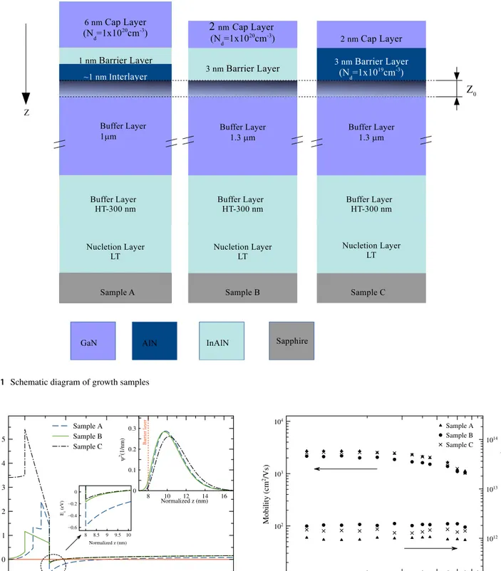
The Hall effect measurements were taken out at tempera-tures ranging from 15 to 350 K under 0.5 T magnetic field. AlN/GaN and InAlN/GaN heterostructures with ultrathin barrier were identically grown by low-pressure MOCVD method on c-face (0001) on a sapphire substrate. Primarily, the substrate surface was annealed for 10 min in H2
ambi-ent at 1050 °C with a view to providing the substrate sur-face clean. Then, 15 nm AlN nucleation layer was grown at low temperature (LT) of 770 °C to increase the lattice-match between GaN and sapphire. In the next step, about ~ 1.3 μm undoped GaN layer was grown at 1100 °C. Bar-rier layers of samples A, B and C were grown on undoped 1 nm In0.17Al0.83N at 890 °C, undoped 3 nm In0.17Al0.83N
at 830 °C, 1 × 1019 cm−3 Si-doped 3 nm AlN at 1100 °C,
respectively. For all the samples, the cap layers were grown at 830 °C. The cap layer thickness of samples A, B, and C structures are 1 × 1020 cm−3 Si-doped 6 nm GaN, 1 x 10²⁰
cm−3 Si-doped 2 nm GaN and undoped 2 nm GaN,
respec-tively. To eliminate the alloy disorder scattering resulting from barrier layer for sample A, about 1 nm AlN interlayer was grown between the In0.17Al0.83N barrier and GaN buffer
layers. Figure 1 shows the layer diagram of the studied sam-ples. In Fig. 1, Z0 is schematically represented as the location
of 2DEG in quantum well between ultrathin barrier and buffer layers.
3 Results and discussion
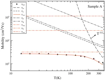
2DEG transport properties of the GaN-based heterostruc-tures with ultrathin InAlN and AlN barrier are investigated in this study. Moreover, the aim of the study is to compare the effect of different barrier layers, as well. First of all, the conduction band energy diagrams of each sample have been calculated by means of TiberCAD software [21]. The numerical calculation details can be found in our previous studies [22]. Figure 2 shows the energy band calculations and the electron probability densities. It is shown that inves-tigated samples have a quasitriangular 2DEG quantum wells between ultrathin barrier and GaN buffer layers. Sample B and sample C have exhibited similar 2DEG quantum wells, and sample A has a wider 2DEG quantum well.
Also, the electron probability densities (ψ2) of
hetero-structures are shown in insert of Fig. 1. The electron dis-tribution of sample B is closer than other investigated het-erostructures. Therefore, sample B is may be more affected from interface roughness scattering.
Figure 3 shows the temperature-dependent sheet carrier densities and the electron mobilities of studied samples which are carried out as the Hall measurements. As shown the sheet carrier density is constant versus the increasing temperature. Although the electron mobilities of the stud-ied samples are constant at low temperature, they decreased proportionally with ~ T−3/2 due to the phonon scattering at
high temperature. It is known that these behaviors accord-ing to the temperature of the sheet carrier density and the electron mobility are typically evidence of the 2DEG at heterointerface.
Sample A has a lower sheet carrier density due to a thin-ner barrier layer thickness than other studied samples. Previ-ously, Jeganathan et al. mentioned that heterostructures with the tensile-strained AlN ultrathin barrier have a low sheet carrier density because of the surface depletion of accumu-lated charge carriers at the heterointerface [16]. Also, the increasing AlN barrier layer thickness will increase the sheet carrier density of 2DEG; however, 2DEG mobility will be decreased and the strain relaxation could occur in the struc-ture. Sample A has the electron mobility higher than other studied samples owing to AlN interlayer which is about 1 nm between the InAlN barrier layer and the GaN channel layer. Since samples B and C have a high sheet carrier density compared with sample A, as expected their electron mobil-ity is lower. The sheet carrier densmobil-ity and electron mobilmobil-ity values of samples A, B, and C are listed in Table 1.
The sheet carrier density and 2DEG mobility of hetero-structures for the different thickness of the ultrathin barrier
layer are reported in several studies Refs. [1, 3, 19]. In these studies, the 2DEG mobility values between 330 and 1450 cm2/V s are found for different AlN and InAlN
bar-rier layer thicknesses. At room temperature, all structures
exhibited lower 2DEG mobilities compared to our samples except the structure with 2.4-nm AlN barrier layer. The low-temperature 2DEG mobilities of the structures are higher than our results and the low-temperature 2DEG mobilities
Fig. 1 Schematic diagram of growth samples
5 10 15 20 25 30 1 0 1 2 3 4 5 Normalized z (nm) Ec (eV) Sample A Sample B Sample C 8 10 12 14 16 0 0.1 0.2 0.3 Normalized z (nm) 2(1/nm) Barrier layer 8 8.5 9 9.5 10 0.6 0.4 0.2 0 Normalized z (nm) Ec (eV)
Fig. 2 The conduction band energy diagrams for studied samples
100 200 300 400 500 10 102 103 104 T(K) Mobility (c m 2/Vs) Sample A Sample B Sample C 1012 1013 1014
Sheet Carrier Densit
y (c
m
-2)
Fig. 3 Electron mobility and sheet carrier density of samples A, B,
are related to the interface roughness of the heterointerface of the related 2DEG populates. This is well known that inter-face roughness is one of the most important scattering mech-anisms on 2DEG at low temperature [23]. The lower 2DEG mobility can be explained with the difference in growth methods of the structures because it is known that GaN-based heterostructures grown using MBE have a smoother interface than heterostructures grown using MOCVD method [24]. The scattering analyses of the 2DEG mobility have been carried out depending on the Matthiessen’s rule which is the sum of the individual scattering mechanisms. Here, μHall and μtot are Hall and the total of calculated
mobil-ities, and μpo, μpe, μdp, μimp, μifr, μac, μrem, μall are mobilities
corresponding to the polar optical phonon, the piezoelectric, the deformation potential, the impurity, the interface rough-ness, the acoustic phonon, the remote impurity, and the alloy disorder scattering mechanisms, respectively. In the results of the calculations, the fitting parameters such as deforma-tion potential constant (Ξ), quantum well width (Z0), and
correlation length (Λ) are given by Table 2.
In the calculations, the lateral size (Δ) and the background impurity (nimp) were taken 2.58 × 10⁻¹⁰ m (one monolayer)
and 1023 m−3 [25], respectively. For each sample, the
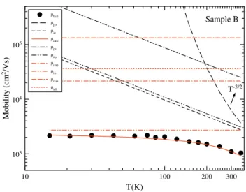
analy-sis of the scattering mechanisms has been made using the required constants and formulas given in Refs. [26–28]. It is shown that the 2DEG mobility is dominated by the interface roughness scattering mechanism at the low temperature in the studied samples. It is known that the narrower quantum wells are more affected by the interface roughness scatter-ing [29]. As can be shown in Tables 1 and 2, the 2DEG
mobility is lower in the narrow quantum wells. On the other hand, this relation between the width of quantum well and 2DEG mobility can be shown in Fig. 2 because sample A has a wider quantum well and has a higher 2DEG mobility at low temperature.
Figure 4 shows the calculated and the Hall mobility of sample A. While the electron mobility is confined by the interface roughness scattering at low temperatures, it is strongly limited by the polar optical phonon scattering at high temperatures. Also, it is shown that the acoustic pho-non-scattering mechanism is relatively dominated by the electron mobility in the middle temperatures as well.
The 2DEG scattering analysis of sample B is shown in Fig. 5. Although the electron mobility is dominated by the interface roughness scattering in almost all temperatures, as expected the acoustic phonon-scattering mechanisms are dominated at the middle temperature [30–33]. As shown from Fig. 2, the electron probability density of sample B is the closest to barrier layer compared with other studied samples. It is shown that sample B has been affected by
Table 1 Sheet carrier density and electron mobility values of samples A, B, and C
Sample Sheet carrier density (cm−2) Mobility (cm2/V s) Growth method Barrier
layer thick-ness 15 K 300 K 15 K 300 K A 1.03 × 10¹² 9.6 × 10¹¹ 2721 1193 MOCVD 1 B 1.77 × 10¹² 1.97 × 10¹² 2159 1101 MOCVD 3 C 1.49 × 10¹² 1.34 × 10¹² 2510 1246 MOCVD 3 [31] – 2 × 10¹³ – 320 MOCVD 11 [1] – 1.9 × 10¹³ – 1180 MBE 1 [3] 2.6 × 10¹³ (77 K) 2.9 × 10¹³ 5032 (77 K) 1213 MBE 3.5 [19] 1.5 × 10¹³ (77 K) 1.55 × 10¹³ 4950 (77 K) 1450 MBE 2.4 [19] 2.5 × 10¹³ (77 K) 2.6 × 10¹³ 2300 (77 K) 920 MBE 3.7 [19] 3.6 × 10¹³ (77 K) 5.6 × 10¹³ 660 (77 K) 330 MBE 4.9
Table 2 Quantum well parameters of studied samples
Sample Z0 (nm) Ξ (eV) Λ (nm) A 2.0 40 4.77 B 1.0 50 9.22 C 1.6 38 4.77 100 200 300 10 103 104 105 T(K) Mobility (c m 2/Vs) hall po ac calc. pe dp imp ifr rem Sample A T-3/2
interface roughness scattering mechanism at low tempera-ture and this result is confirmed by 2DEG probability den-sity results. Compared with the other samples, 2DEG mobil-ity is more affected by the acoustic phonon scattering in sample B. As expected, 2DEG mobility is dominated by the polar optical phonon-scattering mechanism, as well as these scattering mechanisms, at high temperatures. Moreover, it is important that the four scattering mechanisms are dominated by almost equal rate on the 2DEG mobility at the tempera-ture of 350 K. Therefore, there is no sharp decrease in the electron mobility compared with sample C and sample A at high temperature. Also, in this structure, the alloy disorder scattering mechanism has been considered in terms of the correct scattering analysis because the electrons in the 2D quasitriangular quantum well may be scattered due to the alloy barrier layer.
The scattering analysis of 2DEG which is populated in sample C is shown in Fig. 6. There are two important scat-tering mechanisms that are limiting the electron mobility. These are the interface roughness at low temperatures and the polar optic phonon-scattering mechanisms at high tem-peratures. It can be seen that the acoustic scattering is rela-tively effective on electron mobility at around 200 K. The remote impurity scattering in sample C is regarded because of Si-doped barrier layers. But it can be clearly seen that there is no effect of the remote impurity scattering on the 2DEG mobility.
4 Conclusion
In this study, first, the Hall effect measurements of AlN/ GaN and In0.17Al0.83N/GaN with ultrathin barrier grown by
MOCVD have been carried out in the temperature range of 15–350 K and at a constant magnetic field of 0.5 T. As
a result of the measurements, the sample with the highest sheet carrier density is sample B due to usage of the mod-ulation-doped cap layer, although sample A has the high-est electron mobility among the studied samples owing to effect of about 1 nm AlN interlayer. As a result of the 2DEG scattering using Hall mobility data, it is determined that the interface roughness is the dominant scattering mecha-nism at low temperatures while polar optical phonon is the dominant scattering mechanism for the samples at high temperatures. Moreover, the deformation potential and the acoustic phonon-scattering mechanisms relatively limited the 2DEG mobility at the middle temperatures. Besides the experimental measurements, the conduction energy band has been calculated for each sample. According to numerical calculations, quasitriangular quantum well formations and 2DEG probability densities of the studied structures have been investigated. 2DEG formation in a 2D quasitriangu-lar quantum well is shown in each studied samples. 2DEG probability density of sample B is closer than other samples and experimental results confirmed that sample B is more affected from interface roughness scattering mechanism. The fitting parameters such as the quantum well width, the correlation length and the deformation potential values for each sample have been calculated. Finally, when the AlN/ GaN is compared with ultrathin barrier heterostructures and conventional InAlN/GaN and AlGaN/GaN heterostructures, it has exhibited similar sheet carrier density and the Hall mobility, though it had an ultrathin barrier layer. It could be shown that using the AlN barrier layer has a positive effect on the transport properties of the 2DEG.
Acknowledgements One of the authors (E.O.) also acknowledges partial support from the Turkish Academy of Sciences. This research was supported in part by the Distinguished Young Scientist Award of Turkish Academy of Sciences (TUBA-GEBIP 2016).
100 200 300 10 103 104 105 T(K) Mobility (c m 2/Vs) hall po ac calc. pe dp imp ifr rem all Sample B T-3/2
Fig. 5 Scattering analysis of sample B depending on the temperature
100 200 300 10 103 104 105 T (K) Mobility (c m 2/Vs) hall po ac calc. pe dp imp ifr rem Sample C T-3/2
References
1. C. Ostermaier, G. Pozzovivo, J.F. Carlin, B. Basnar, W. Schrenk, Y. Douvry, C. Gaquire, J.C. DeJaeger, K. Cico, K. Fröhlich, M. Gonschorek, N. Grandjean, G. Strasser, D. Pogany, J. Kuzmik, Ultrathin InAlN/AlN barrier HEMT with high performance in normally off operation. IEEE Electron. Device Lett. 30, 1030– 1032 (2009)
2. F. Medjdoub, M. Zegaoui, N. Rolland, P.A. Rolland, Demonstra-tion of low leakage current and high polarizaDemonstra-tion in ultrathin AlN/GaN high electron mobility transistors grown on silicon substrate. Appl. Phys. Lett. 98(22), 223502 (2011)
3. Y. Cao, D. Jena, High-mobility window for two-dimensional electron gases at ultrathin AlN∕GaN heterojunctions. Appl. Phys. Lett. 90(18), 182112 (2007)
4. L. Shen, S. Heikman, B. Moran, R. Coffie, N.Q. Zhang, D. But-tari, I.P. Smorchkova, S. Keller, S.P. DenBaars, U.K. Mishra, AlGaN/AlN/GaN high-power microwave HEMT. IEEE Elec-tron. Device Lett. 22, 457–459 (2001)
5. O. Ambacher, J. Smart, J.R. Shealy, N.G. Weimann, K. Chu, M. Murphy, W.J. Schaff, L.F. Eastman, R. Dimitrov, L. Wittmer, M. Stutzmann, W. Rieger, J. Hilsenbeck, Two-dimensional electron gases induced by spontaneous and piezoelectric polarization charges in N-and Ga-face AlGaN/GaN heterostructures. J. Appl. Phys. 85, 3222–3233 (1999)
6. D.F. Storm, D.A. Deen, D.S. Katzer, D.J. Meyer, S.C. Binari, T. Gougousi, T. Paskova, E.A. Preble, K.R. Evans, D.J. Smith, Ultrathin-barrier AlN/GaN heterostructures grown by rf plasma-assisted molecular beam epitaxy on freestanding GaN substrates. J. Cryst. Growth 380, 14–17 (2013)
7. A. Teke, S. Gökden, R. Tülek, J.H. Leach, Q. Fan, J. Xie, Ü. Özgür, H. Morkoç, S.B. Lisesivdin, E. Özbay, The effect of AlN interlayer thicknesses on scattering processes in lattice-matched AlInN/GaN two-dimensional electron gas heterostructures. New J. Phys. 11, 063031 (2009)
8. M.N. Gurusinghe, S.K. Davidsson, T.G. Andersson, Two-dimensional electron mobility limitation mechanisms in AlxGa1 − xN∕GaN heterostructures. Phys. Rev. B 72, 045316 (2005)
9. E. Arslan, S. Bütün, S.B. Lisesivdin, M. Kasap, S. Ozcelik, E. Ozbay, The persistent photoconductivity effect in AlGaN/GaN heterostructures grown on sapphire and SiC substrates. J. Appl. Phys. 103, 103701 (2008)
10. P. Tasli, B. Sarikavak, G. Atmaca, K. Elibol, A.F. Kuloglu, S.B. Lisesivdin, Numerical simulation of novel ultrathin bar-rier n-GaN/InAlN/AlN/GaN HEMT structures: effect of indium-mole fraction, doping and layer thicknesses. Phys. B 405, 4020– 4026 (2010)
11. M. Gonschorek, J.F. Carlin, E. Feltin, M.A. Py, N. Grandjean, High electron mobility lattice-matched AlInN∕GaN field-effect transistor heterostructures. Appl. Phys. Lett. 89, 062106 (2006) 12. H.G. Xing, D. Deen, Y. Cao, T. Zimmermann, P. Fay, D. Jena,
MBE-grown ultra-shallow AlN/GaN HFET technology. ECS Trans. 11, 233–237 (2007)
13. G. Martin, A. Botchkarev, A. Rockett, H. Morkoc, Valence-band discontinuities of wurtzite GaN, AlN, and InN heterojunctions measured by X-ray photoemission spectroscopy. Appl. Phys. Lett. 68, 2541–2543 (1996)
14. A. Bourret, C. Adelmann, B. Daudin, J.L. Rouvière, G. Feuillet, G. Mula, Strain relaxation in (0001) AlN/GaN heterostructures. Phys. Rev. B 63, 245307 (2001)
15. A.M. Sanchez, F.J. Pacheco, S.I. Molina, J. Stemmer, J. Ader-hold, J. Graul, Critical thickness of high-temperature AIN interlayers in GaN on sapphire (0001). J. Electron. Mater. 30, L17–L20 (2001)
16. K. Jeganathan, T. Ide, M. Shimizu, H. Okumura, Strain relaxa-tion correlated with the transport properties of AlN/GaN het-erostructure grown by plasma-assisted molecular-beam epitaxy. J. Appl. Phys. 93, 2047–2050 (2003)
17. T. Koyama, M. Sugawara, Y. Uchinuma, J.F. Kaeding, R. Sharma, T. Onuma, S. Nakamura, S.F. Chichibu, Strain relaxa-tion in NH3 source molecular beam epitaxy of AlN epilayers on GaN epitaxial templates. Phys. Status Solidi (a) 203, 1603–1606 (2006)
18. Y. Cao, K. Wang, A. Orlov, H. Xing, D. Jena, Very low sheet resistance and Shubnikov–de-Haas oscillations in two-dimen-sional electron gases at ultrathin binary AlN∕ GaN heterojunc-tions. Appl. Phys. Lett. 92, 152112 (2008)
19. I.P. Smorchkova, S. Keller, S. Heikman, C.R. Elsass, B. Heying, P. Fini, J.S. Speck, U.K. Mishra, Two-dimensional electron-gas AlN/GaN heterostructures with extremely thin AlN barriers. Appl. Phys. Lett. 77, 3998–4000 (2000)
20. G. Atmaca, S. Ardali, E. Tiras, T. Malin, V.G. Mansurov, K.S. Zhuravlev, S.B. Lisesivdin, Scattering analysis of 2DEG mobil-ity in undoped and doped AlGaN/AlN/GaN heterostructures with an in situ Si3N4 passivation layer. Solid State Electron.
118, 12–17 (2016)
21. M. Auf der Maur, M. Povolotskyi, F. Sacconi, A. Pecchia, G. Romano, G. Penazzi, A. Di Carlo, Opt. Quantum Electron.
40(14), 1077–1083 (2008)
22. G. Atmaca, P. Narin, B. Sarikavak-Lisesivdin, S.B. Lisesivdin, Two dimensional electron gas in a hybrid GaN/InGaN/ZnO heterostructure with ultrathin InGaN channel layer. Phys. E 79, 67–71 (2016)
23. U. Penner, H. Rücker, I.N. Yassievich, Theory of interface roughness scattering in quantum wells. Semicond. Sci. Technol.
13, 709–713 (1998)
24. Y. Zhang, I.P. Smorchkova, C.R. Elsass, S. Keller, J.P. Ibbetson, S. Denbaars, U.K. Mishra, J. Singh, Charge control and mobility in AlGaN/GaN transistors: experimental and theoretical studies. J. Appl. Phys. 87, 7981–7987 (2000)
25. G.Y. Zhang, Y.Z. Tong, Z.J. Yang, S.X. Jin, J. Li, Z.Z. Gan, Relationship of background carrier concentration and defects in GaN grown by metalorganic vapor phase epitaxy. Appl. Phys. Lett. 71, 3376–3378 (1997)
26. D. Zanato, S. Gokden, N. Balkan, B.K. Ridley, W.J. Schaff, The effect of interface-roughness and dislocation scattering on low temperature mobility of 2D electron gas in GaN/AlGaN. Semicond. Sci. Technol. 19, 427–432 (2004)
27. S. Gökden, Mobility of two-dimensional electrons in an AlGaN/ GaN modulation-doped heterostructure. Phys. Status Solidi (a)
200, 369–377 (2003)
28. S.B. Lisesivdin, S. Acar, M. Kasap, S. Ozcelik, S. Gokden, E. Ozbay, Scattering analysis of 2DEG carrier extracted by QMSA in undoped Al0.25Ga0.75N/GaN Heterostructures. Semicond. Sci.
Technol. 22, 543–548 (2007)
29. J.M. Li, J.J. Wu, X.X. Han, Y.W. Lu, X.L. Liu, Q.S. Zhu, Z.G. Wang, A model for scattering due to interface roughness in finite quantum wells. Semicond. Sci. Technol. 20, 1207–1212 (2005)
30. S. Gökden, A. Ilgaz, N. Balkan, S. Mazzucato, The effect of scattering mechanisms on the low field mobility in GaN/AlGaN heterostructures. Phys. E 25, 86–92 (2004)
31. R. Gaska, J.W. Yang, A. Osinsky, Q. Chen, M.A. Khan, A.O. Orlov, G.L. Snider, M.S. Shur, Electron transport in AlGaN– GaN heterostructures grown on 6H–SiC substrates Appl. Phys. Lett. 72, 707–709 (1998)
32. D. Huang, F. Yun, M.A. Reshchikov, D. Wang, H. Morkoc, D.L. Rode, L.A. Farina, Ç. Kurdak, K.T. Tsen, S.S. Park, K.Y. Lee, Hall mobility and carrier concentration in free-standing high
quality GaN templates grown by hydride vapor phase epitaxy. Solid State Electron. 45(5), 711–715 (2001)
33. D. Huang, F. Yun, M.A. Reshchikov, D. Wang, H. Morkoc, D.L. Rode, L.A. Farina, Ç. Kurdak, K.T. Tsen, S.S. Park, K.Y. Lee, Low interface state density AlN/GaN MISFETs. Electron. Lett.
35, 2145–2146 (1999)
Publisher’s Note Springer Nature remains neutral with regard to jurisdictional claims in published maps and institutional affiliations.