Large-area semi-transparent light-sensitive nanocrystal
skins
Shahab Akhavan1, Burak Guzelturk1, Vijay Kumar Sharma1, and Hilmi Volkan Demir1,2,*
1UNAM–Institute of Materials Science and Nanotechnology, Department of Electrical and Electronics Engineering, Department of Physics, Bilkent University, Ankar, 06800, Turkey
2School of Electrical and Electronic Engineering, School of Physical and Mathematical Sciences, Nanyang Technological University, Singapore, 639798, Singapore
Abstract
Large area and semi-transparent highly light sensitive nanocrystal skin is demonstrated via spray-coating nanocrystals on top of polyelectrolyte-polymers based on photogenerated potential buildup where no external bias is applied.
Nanocrystals (NCs) synthesized using wet chemistry are considered as primary components of future optoelectronic devices [1,2]. Bandgap tunability in which optical absorption and emission can be adjusted through the quantum size effect, together with the ability to deposit easily via spray coating, dip-coat and spin- coat at reduced costs over large area where lattice mismatch does not arise, make them promising materials for
integrating them into the optoelectronic devices. In this work, we demonstrate large area (48 cm2),
semi-transparent, light sensitive nanocrystal skins (LS-NS) composed of a single monolayer CdTe NC, which is highly sensitive to UV and visible light (Fig. 1a). Moreover, by selecting appropriate bandgap of NCs, operation of the device can be further extended to infrared, e.g. in the case of CdHgTe NCs. High sensitivity in the absence of external bias is due to the close interaction of NCs with the top contact while the other part is isolated using high dielectric spacing layer. Furthermore, since NCs are sealed by the metal contact, the resulting device becomes highly stable in ambient condition. Hence, using monolayer of NCs, while providing sufficient
absorption results in semi-transparency, reduce noise generation and dark current.
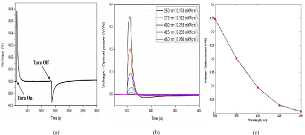
After electron and hole pair generation, charges are not allowed to pass through the device and due to the device architecture and work function of NCs and top metal Al, holes are accumulated at this contact. Metal contact acts as a hole acceptor, while electrons are trapped inside NCs. Fig. 2a illustrates the mechanism of the device under light illumination at 350 nm (0.175 mW) for varying period of time. As it can be seen, photocharge buildup results in generating voltage up to the peak point after which the voltage buildup diminishes over time due to the change in the effective dielectric constant of the monolayer CdTe NC and absorption saturation. Decreases in the voltage builup continue until the steady state is reached where trapping leads to almost equal amount of storage charge. By just switching off the light, decrease in the potential buildup observed due to the absence of charge storage potential and presence of the trapped charge effect. Consequently, this behavior shows the ability to measure the amount of charge trapped inside the NCs and time it takes to sweep out these charges. We observed that a higher voltage buildup can be obtained at a shorter wavelength due to the higher absorption of CdTe NCs where more states are available for electron and hole pair generation. Obtained result is in agreement with the CdTe absorption spectrum (Fig. 2b and 2c). Here, the device exhibits a larger negative voltage for a shorter wavelength of light and takes more time to relax these charges in the absence of light due to the increased number of trapped charges owing to the increased absorption. Furthermore, we show that through shining light on the device, an exponential decay is replaced with a decay that shows non-linear behavior in this light sensitive device. This behavior is in strong agreement with the diminishing voltage buildup after reaching the peak point. As a proof-of-concept demonstration, we also studied ligand removal to minimize transit time and maximize mobility, which strongly enhance the sensitivity and accelerate the photocurrent decay. We observed a substantial enhancement of 79% in the light sensitivity and a 3-fold shortened photocurrent decay time from 300
ms to <100 ms. Furthermore, the minimum noise equivalent intensity decreased from 1.94 W/cm2 when the
ligands were present to 0.443 W/cm2 when the ligands were removed, indicating a faster charge transfer with
the ligand removal.
In conclusion, we demonstrated large area (48 cm2), solution processed light sensitive nanocrystals skin via
spraying NCs on the polyelectrolyte polymers that avoid the need for any external bias. In this device design, NCs are placed exactly below the top metal contact, resulting in close interaction with the electrode, fast charge transit time, and sealing (which enhance the device stability under ambient condition). Furthermore, LS-NS is composed of only a single monolayer of CdTe NC which results in using a small amount of material, making the device semi transparent, allowing for easier surface functionalization and reduction in generation recombination noise and dark current.
479
WH2 (Contributed Oral) 8:45 AM – 9:00 AM
(a) (b)
Fig. 1. (a) Large area LS-NS, 8 cm 6 cm in size, (b) a scheme of LS-NS composed of a monolayer of TGA capped CdTe NCs on the top of polyelectrolyte polymers (PDDA and PSS): (1) direction of charge accumulation (2) trapped effect, and (3) exponential decay
(a) (b) (c)
Fig. 2. (a) Changes in the voltage buildup via switching the light on and off at 350 nm (0.153 mW) (b) sensitivity of LS-NS operating at different wavelengths with different intensities (c) maximum sensitivity of the LS-NS as a function of operating wavelength.
References
1. H. V. Demir, S. Nizamoglu, E. Mutlugun, T. Özel, S. Sapra, N. Gaponik, A. Eychmüller, "Tuning shades of white light with multi-color quantum-dot-quantum-well emitters based on onion-like CdSe- ZnS heteronanocrystals," Nanotechnology 19, 335203 (2008).
2. E. Mutlugun, I. M. Soganci, and H. V. Demir, “Nanocrystal hybridized scintillators for enhanced detection and imaging on Si platforms in UV,” Opt. Express 15(3), 1128-1134 (2007).
480 View publication stats