SIZE AND COMPOSITION MODULATED
SUPERLATTICES OF SILICON BASED
NANOWIRES
a thesis
submitted to the program of material science and
nanotechnology
and the institute of engineering and science
of bilkent university
in partial fulfillment of the requirements
for the degree of
master of science
By
Seymur Cahangirov
July, 2008
I certify that I have read this thesis and that in my opinion it is fully adequate, in scope and in quality, as a thesis for the degree of Master of Science.
Prof. Dr. Salim C¸ ıracı (Advisor)
I certify that I have read this thesis and that in my opinion it is fully adequate, in scope and in quality, as a thesis for the degree of Master of Science.
Prof. Dr. Engin Akkaya
I certify that I have read this thesis and that in my opinion it is fully adequate, in scope and in quality, as a thesis for the degree of Master of Science.
Assist. Prof. Ramazan Tu˘grul Senger
Approved for the Institute of Engineering and Science:
Prof. Dr. Mehmet B. Baray
Director of the Institute Engineering and Science
ABSTRACT
SIZE AND COMPOSITION MODULATED
SUPERLATTICES OF SILICON BASED NANOWIRES
Seymur Cahangirov
M.S. in Material Science and Nanotechnology Supervisor: Prof. Dr. Salim C¸ ıracı
July, 2008
Mechanical properties, atomic and energy band structures of bare and hydrogen passivated SinGen nanowire superlattices have been investigated by using
first-principles pseudopotential plane wave method. Undoped, tetrahedral Si and Ge nanowire segments join pseudomorphically and can form superlattice with atom-ically sharp interface. Upon heterostructure formation, superlattice electronic states form subbands in momentum space. Band lineups of Si and Ge zones re-sult in multiple quantum wells, where specific states at the band edges and in band continua are confined. The electronic structure of the nanowire superlat-tice depends on the length and cross section geometry of constituent Si and Ge segments. Also we showed that hydrogen saturated silicon nanowires of differ-ent diameters having differdiffer-ent band gaps can form stable junctions. Superlattices formed by the periodically repeated junctions of silicon nanowire segments having different lengths and diameters exhibit electronic states which can be confined in regions having either narrow or wide parts of superlattice. A point defect, such as a missing atom or substitutional impurities with localized states near band edges can make modulation doping possible. Since bare Si and Ge nanowires are metallic and the band gaps of hydrogenated ones varies with the diameter, these superlattices offer numerous options for multiple quantum well devices with their leads made from the constituent metallic nanowires. Finally, we have con-sidered the junction between bare and hydrogenated nanowires to realise metal-semiconductor heterostructure. We have treated this heterostructure within the supercell geometry and deduced the formation of Schottky barrier. We have shown that Si and Ge nanowires can bring about a novel concept in nanocircuit, where interconnects, devices etc are produced on a single rode.
Keywords: ab initio, density functional theory, nanowire, superlattice.
¨
OZET
B ¨
UY ¨
UKL ¨
UK VE S¸EK˙IL MOD ¨
ULASYONLU S˙IL˙ISYUM
TABANLI NANOTEL S ¨
UPER ¨
ORG ¨
ULER
Seymur Cahangirov
Malzeme Bilimi ve Nanoteknoloji , Y¨uksek Lisans Tez Y¨oneticisi: Prof. Dr. Salim C¸ ıracı
Temmuz, 2008
Hidrojenle doyurulmu¸s SinGen nanotel s¨uper¨org¨ulerin mekanik ¨ozellikleri,
atomik ve enerji band yapısı temel prensiplerle, pseudo potansiyel ve d¨uzlemsel dalga y¨ontemiyle incelendi. Katkısız, tetrahedral Si ve Ge nanoteller ya-pay olarak birle¸sebilmekte ve atomik seviyede keskin aray¨uzl¨u s¨uper¨org¨u olu¸sturabilmektedir. Heteroyapı olu¸sumuyla birlikte, s¨uper¨org¨uye ait elektronik durumlar momentum uzayında bant olu¸sturmaktadır. Si ve Ge b¨olgesindeki bant-ların sıralanması sonucu ¸coklu kuantum kuyuları olu¸smakta ve bazı durumlar bu kuyularda yo˘gunla¸smaktadır. Ayrıca, farklı ¸caplara sahip hidrojenle doyu-rulmu¸s silisyum nanotellerin ba˘glanarak kararlı yapı olu¸sturdu˘gu g¨ozlemlenmi¸stir. Farklı ¸cap ve uzunluktaki silisyum nanotellerin periyodik olarak birle¸smesi sonucu olu¸san s¨uper¨org¨uler ilgin¸c elektronik ¨ozellikler g¨ostermektedir. Bazı elektronik durumlar kalın ya da ince kısımda yo˘gunla¸sabilmektedir. Eksik bir atom ya da yerine ba¸ska atomun ge¸cmesi sonucu olu¸san noktasal bozukluklar bant kenarında yerel durumlara neden olmakta ve bu da mod¨ulasyon katkılamayı m¨umk¨un kılmaktadır. C¸ ıplak Si ve Ge nanotellerin metalik ¨ozellik ta¸sıması ve hidro-jenle doyurulanların yasak enerji aralı˘gının i¸cerik ve yarı¸capa g¨ore de˘gi¸smesi bu yapıların ¸coklu kuantum kuyusu aygıtı olarak kullanılabilece˘gini ve ba˘glantıların metalik nanotellerle yapılabilece˘gini g¨ostermektedir. Son olarak, ¸cıplak ve hidro-jenle doyurulmu¸s silisyum nanotellerin birle¸smesiyle olu¸san metal-yarıiletken het-eroyapılar incelendi. Bu hethet-eroyapılar s¨uperh¨ucre geometrisiyle ele alındı ve Schottky bariyeri olu¸sumu sonucuna varıldı. Nanoelektronikte yeni bir konsept olarak, Si ve Ge nanotellerin kullanımıyla tek tel ¨uzerinde ba˘glantılar, devreler ve s. yapımının m¨umk¨un oldu˘gu g¨osterildi.
Anahtar s¨ozc¨ukler : ab initio, yo˘gunluk fonksiyonu teorisi, nanotel, s¨uper¨org¨u.
Acknowledgement
I would like to express my deepest gratitude to my supervisor Prof. Dr. Salim C¸ ıracı for his priceless guidance. He is the only person I know, who mixes ad-ministration and politeness in perfect ratios.
I would like to thank Dr. Engin Durgun for sharing his life and research experience as a friend and scientist.
I would like to thank Dr. Haldun Sevin¸cli, who always had answers to my science questions.
I would like to thank my friends and research partners Mehmet Topsakal, Can Ataca, Erman Bekaro˘glu and Hasan S¸ahin for wonderful time I had with them during research. Also I would like to thank all my friends in the Institute of Material Science and Nanotechnology and Department of Physics.
I would like to thank people of Azerbaijan where I have grown up and hos-pitable people of Turkey where I had my undergraduate and graduate education. Special thanks go to my parents, my brother and my sister and all other relatives support of whom I always felt behind me.
Finally I would like to thank and dedicate this thesis to my wife Naide for sharing her life with me.
Contents
1 Introduction 1
1.1 Motivation . . . 3
1.2 Organization of the Thesis . . . 4
2 Silicon and Germanium Nanowires 5 2.1 Structure . . . 7
2.2 Electronic Properties . . . 7
2.3 Synthesis of Nanowire Superlattices . . . 8
3 Theoretical Background 9 3.1 Density Functional Theory . . . 9
3.1.1 Hohenberg-Kohn Formulation . . . 9
3.1.2 Kohn-Sham Equations . . . 10
3.2 Exchange and Correlation . . . 12
3.2.1 Local Density Approximation (LDA) . . . 12
3.2.2 Generalized Gradient Approximation (GGA) . . . 12 vi
CONTENTS vii
3.3 Pseudopotential Approximation . . . 13
4 SinGen Nanowire Superlattices 14
4.1 Introduction . . . 14 4.2 Method of calculations . . . 16 4.3 Bare and Hydrogenated Nanowires and Nanowire Superlattices . . 18 4.4 Mechanical properties . . . 21 4.5 Electronic Properties . . . 25 4.6 Confined states . . . 29
5 Size Modulated Si NWSL 32
5.1 Calculations and Results . . . 32
6 Metal-Semiconductor Heterostructure 40
List of Figures
2.1 Ideal, bare and hydrogenated silicon nanowires are presented. Nanowires having 68 (25 and 57) atoms in a unit cell are cut along [111] ([100]) direction. . . 6 2.2 STM images of silicon nanowires grown along [112] and [110]
di-rections, as given in the Ref. [11] . . . 8
3.1 Illustration of all-electron (dashed lines) and pseudoelectron (solid lines) potentials and their corresponding wave functions. . . 13
4.1 Optimized atomic structure of bare and hydrogenated SinGen
nanowire superlattices for n=75 and 114. a) Top view; b) Side view. Small-gray, large-light and large-dark balls correspond to the hydrogen, silicon and germanium atoms respectively. . . 17 4.2 Interatomic distance distribution of optimized bare and
hydro-genated Si2n, Ge2nand SinGenfor n=75 up to fourth nearest
neigh-bor. The similar distribution for Si114Ge114 and H-Si114Ge114 are
also shown. The Si-H (Ge-H) bond lengths being in the range of (∼ 1.5 ˚A) are not shown. . . 20
LIST OF FIGURES ix
4.3 Energy band structures of optimized bare and hydrogenated Si2n,
Ge2n nanowires and SinGen nanowire superlattices for n=75. Zero
of energy is taken at the Fermi level. Band gaps are shown by shaded zones. Dashed and dotted lines (minibands) are obtained by folding of Si50 (also H-Si50) and Ge50 (also H-Ge50) bands. . . . 23
4.4 Energy band structures of optimized bare and hydrogenated Si2n,
Ge2nnanowires and SinGennanowire superlattices for n=114. Zero
of energy is taken at the Fermi level. Dashed and dotted lines are obtained by folding of Si57 (also H-Si57) and Ge57 (also H-Ge57)
bands. . . 24 4.5 Energy band structure of bare and hydrogenated SinGen nanowire
superlattices for n=25, 50 and 57. . . . 26 4.6 Schematic description of energy band diagram in the unit cell (on
the right and upper side), band structure in momentum space (on the left side) and isosurface charge density of states of H-Si75Ge75
NWSL at the band edges. . . 27 4.7 Schematic description of energy band diagram in the unit cell (on
the right and upper side),band structure in the momentum space (on the left side) isosurface charge density of states of H-Si114Ge114
NWSL at the band edges. . . 28
5.1 Energy band structure and charge density isosurfaces of the su-perlattice, Si138H42, formed from periodically repeated junctions
consisting of one unit cell of SiNW with D1 ∼ 11 ˚A and two unit
cell of SiNW with D2 ∼ 7 ˚A formed along [111] direction.
Iso-surfaces of charge density of valence and conduction band states confined at different regions in real space. Large and small balls indicate Si and H atoms. Zero of energy is set at the Fermi level shown by dash-dotted line. . . 34
LIST OF FIGURES x
5.2 (a) Same as Fig. 5.1 for Si157H64formed from periodically repeated
junctions consisting of two unit cell of SiNW with D1 ∼ 14 ˚A and
three unit cell of SiNW with D2 ∼ 7 ˚A formed along [100] direction.
The charge density isosurfaces of the defect state (due to one Si and one H atom attached to it is missing from Si157H64) and the
state below corresponding to the structure Si156H63 is shown in
the dashed box. (b) The distribution of interatomic distances of relaxed superlattice. The arrows indicate the ideal bulk 1st, 2nd and 3rd nearest neighbor distances. . . 36 5.3 Band structure, local density of states (LDOS), charge density
isosurfaces of Al and P (substitutional) doped Si157H64 (namely
Si156P(Al)H64). Here, p and s indicate 3s and 3p projected LDOS
at the impurity atom. Dash-dotted lines indicate the Fermi energy 37
6.1 Band structure and total density of states plots for bare, hydro-gen saturated and superlattice structure. Schematic diagram of band alignment in conventional metal-semiconductor junctions and charge density isosurface plots corresponding to metallic (M), semi-conducting (S) and Schottky barrier (SB) states. . . 41
List of Tables
4.1 Equilibrium values of lattice parameter c are given in units of ˚A. Force constant κ (as defined in the text), in units of eV/˚A, is calculated by using both VASP result and Hook’s law. Percentage difference in between force constant values calculated from VASP result and Hook’s law is given within parenthesis in order to check whether classical Hook’s law is still valid in nanoscale. Also force constant κ0 (as defined in the text) is presented in units of eV. . . 22
Chapter 1
Introduction
Superlattices are heterostructures formed by periodically varying layers of two or more substances. Building blocks of superlattices can be either metals or semi-conductors. Planar semiconductor superlattices were first grown in 1970’s and metallic ones in 1980. In planar semiconductor superlattices, band gap varies periodically in direct space along direction perpendicular to the layers. Because of this geometry, minibands are formed in momentum space perpendicular to the layers. This results in unusual electronic functions for novel devices. Field ef-fect transistors (FETs), photodetectors, light emmiting diodes (LEDs), quantum cascade lasers are few examples of these novel applications.
Nowadays, with the help of new growth techniques one-dimensional (1D) nanowire superlattices are synthesized. These nanowire superlattices have po-tential to combine functions of nanowires and superlattices. The crucial question here is whether superlattice geometry conserves conventional properties when lay-ers with large areas are diminished to nanosize. This will result in LEDs, FETs and other superlattice devices which are not only compatible with well known semiconductor technology but also increase information capacity in enormous range.[1]
One of the most promising applications of nanowires are termoelectric devices.[2] As indicated by Maria Telkes [3], in her 1947 paper, bulk silicon is
CHAPTER 1. INTRODUCTION 2
not efficient as a termoelectric device. This is because silicon is a good heat con-ductor and it can’t prevent heat diffusion, i.e. temperature gradient along the device could not be maintained. However when cross-section is reduced to nano-size thermal conductivity is reduced by 100 times relative to its bulk counterpart. This effect takes place because heat carrying phonons, electrons and holes are faced with obstacles like nanowire edges. Nanowire geometry not only reduces thermal conductivity but also helps to adjust other parameters affecting thermo-electric efficiency like Seebeck coefficient and thermo-electrical resistivity. Recently two independent experimental works [4, 5] indicate that silicon nanowires with cross-section radius of 20-50 nm can be managed to give thermoelectric efficiencies comparable with commercial bismuth-telluride semiconducting thermodevices.[2] Fluorescence in nanowires is also an interesting research area.[6] According to work by Protasenko et al. [7] fluorescence of CdSe nanowires can be controlled by electric field which opens a room for possibility of mobile charge carriers. This finding can open a broad application area in nanoelectronics.
It is also possible to combine semiconducting nanowires with metallic carbon nanotubes in order to get a miniaturized version of conventional Schottky diodes. Hu and Ouyang et al .[8] have synthesized silicon nanowire, carbon nanotube junctions in a catalytic growth procedure. It is shown that these junctions behave as a Schottky diode and what is more interesting is that they have similar zero-bias junction barrier height as macroscopic metal/p-Si junctions, inspite of their nanosize.
Heterojunctions of compositionally modulated n- and p-type nanowires are also realised in several experimental studies. Gudiksen et al .[9] have synthesized compositionally modulated GaAs and GaP nanowires together with modulation doped n-Si/p-Si and n-In/p-In nanowires. Here GaAs gives strong luminescence but GaP does not. Authors claim that this property can be used for the design of an optical nano-barcode. Also they report light emmition, from modulation doped nanowires, as forward bias is applied. This is a realisation of nanoscale LED.
CHAPTER 1. INTRODUCTION 3
reported a realised nanowire field-effect transistor (NWFET) composed of a Si core and Ge shell geometry. They state that performance of Ge/Si NWFETs are of same order of magnitude with similar length carbon nanotube FETs. The importance of this result lies in difficulties of producing uniform semiconducting carbon nanotubes.
In summary, following subjects related to nanowires have been investigated experimentally and/or theoretically;
• Nanosized Thermoelectric Devices
• Polarized Nanoscale Light Emmiting Diodes (NLEDs)
• Nanosized Field Effect Transistors (NFETs)
• Optical Nano-Barcodes
• 1D Electron Waveguides
• Single Electron Devices (Quantum Computation)
• Multiple Quantum Well Devices
• Nano-Interconnects
• Nanosensors
1.1
Motivation
Because of interesting electronic structure they possess, conventional planar su-perlattices drew attention of both scientists and device engineers for past 30 years. During this period of time a new interdisciplinary field - nanotechnology emerged. Nanotechnology not only aims to reduce well known technology to nanoscale but also tries to explore the new application areas, taking advantages of the quan-tum world. While the two-dimensional heterostructures of semiconductors have a subject of active study leading to the discovery of interesting quantizations of
CHAPTER 1. INTRODUCTION 4
electrons in lower dimensionality and fabrication of exotic devices and quantum structures, analogous behaviors are expected to occur in nanowire heterostruc-tures. In this thesis we show that one can preserve superlattice effects in size and compositionally modulated nanowires having diameters of only few nanometers range. We believe that this work will have a considerable impact in both science and device engineering community.
1.2
Organization of the Thesis
The thesis is organized as follows: Chapter 2 summarizes the basic properties and synthesis procedure of silicon and germanium nanowires and superlattices. Chapter 3 gives a brief theoretical background needed for our work. Chapter 4 includes results related to structural, electronic properties of compositionally modulated Si/Ge nanowire superlattices and electron confinement effects in these structures. Chapter 5 consists of results related to size modulated Si nanowire superlattices. Chapter 6 is about bare and hydrogenated silicon nanowire super-lattice heterostructures. Finally, Chapter 7 summarizes and gives some conclusive remarks for this thesis.
Chapter 2
Silicon and Germanium
Nanowires
Nanowires are materials having dimensions of order of nanometer along some plane of their bulk counterparts and grown perpendicular to that plane. Silicon nanowires were grown along [100], [110], [111] and [112] directions in several experimental works.[4, 5, 11] Bare nanowires have very reactive dangling bonds along their surface. These dangling bonds can be passivated by hydrogen, to prevent oxidation. Size of nanowires are defined by either number of atoms in the unitcell along the growth direction or by cross-sectional diameter. Generally this diameter is defined as highest distance between two atoms in the same layer. Although this definition is somewhat ambiguous, it gives an approximate picture for the reader. Core of the nanowires generally conserve bulk structure while surface is recostructed to minimize the total energy by reducing the number of dangling bonds. Nanowire superlattices are formed by joining two different types of nanowires and repeating this periodically. It is important to have a sharp interface between two adjacent parts of nanowire superlattices, i.e., they should be joined pseudomorphically. For Si and Ge nanowires it is possible because they have same bulk crystal structure and similar lattice constants. Wu et al. have synthesized Si/SiGe nanowire superlattice structure by using a hybrid technique which combines pulsed laser ablation and chemical vapor deposition.[12]
CHAPTER 2. SILICON AND GERMANIUM NANOWIRES 6
IDEAL
BARE
HSAT
68
25
57
Figure 2.1: Ideal, bare and hydrogenated silicon nanowires are presented. Nanowires having 68 (25 and 57) atoms in a unit cell are cut along [111] ([100]) direction.
CHAPTER 2. SILICON AND GERMANIUM NANOWIRES 7
2.1
Structure
In ab initio calculations nanowires are generally cut from ideal bulk structure and then fully relaxed until they find a local minima. Then dangling bonds are saturated by hydrogen and structure is again relaxed. However some authors prefer hydrogenation of ideal structures at the beginning. Sometimes these two approaches give different results, but in our respect it is more suitable to choose first method. Fig. 2.1 shows cross-sectional view of silicon nanowires having 25, 57 and 68 atoms per unit cell. As seen here core of nanowires remains similar to ideal case while reconstructions occure at the surface. Surprisingly, sharp edges occure especially at the surface of Si25 nanowires. Normally we would expect
round shapes to be prefered but this sharp structure allows dimerization along the surface and lowers the total energy.[13] Generally, cross-section of nanowires be-come smoother after hydrogenation. Structure of germanium nanowires are very similar to silicon nanowires, except longer bond distances. Since both nanowires have similar structure and lattice constant they can form atomically sharp inter-faces. More detailed treatment of structural and mechanical properties of Si/Ge nanowire superlattices are left to Chapter 4.
2.2
Electronic Properties
Since core of the nanowires preserve bulk geometry, these atoms result in bulk-like electronic properties. However, surface states change the overall electronic behaviour fundamentally. Generally these states have higher dispersion and play important role in making bare nanowires metallic. Saturation of dangling bonds on the surface of silicon and germanium nanowire prevents these surface states and as a result we get a semiconducting nanowire. While bulk silicon and ger-manium have indirect band gaps, nanowires of silicon and gerger-manium generally
CHAPTER 2. SILICON AND GERMANIUM NANOWIRES 8
Figure 2.2: STM images of silicon nanowires grown along [112] and [110] direc-tions, as given in the Ref. [11]
have direct band gaps what makes them potential candidates for optical devices.
2.3
Synthesis of Nanowire Superlattices
There are several ways to synthesize nanowires and nanowire superlattices. One way is to use, vapour-liquid-solid process with a metal catalyst, generally gold nanoparticles. In this method nanoparticles control the diameter of nanowires. This method gives good results for compositionally modulated nanowire super-lattices. GaAs/GaP and InAs/InP nanowire superlattices were synthesized by this method with a diameter as small as 20 nm.[9, 14] Another way is to use su-perlattice nanowire pattern transfer method. Using this method one can adjust dimensions, impurity doping levels and crystallographic nature of silicon based nanowires.[4] Hybrid methods like one used in Ref. [12] also give good results for nanowire superlattices. Silicon nanowires fabricated by oxide-assisted growth method [11, 15, 16] are shown in Fig.2.2. These nanowires can have diameters as small as 1 nm.
Chapter 3
Theoretical Background
3.1
Density Functional Theory
The initial work on Density Functional Theory (DFT) was reported in two pub-lications: first by Hohenberg-Kohn in 1964 [17], and the next by Kohn-Sham in 1965.[18] This was almost 40 years after Schrodinger (1926) had published his pioneering paper marking the beginning of wave mechanics. Shortly after Schrodinger‘s equation for electronic wave function, Dirac declared that chem-istry had come to an end since all its content was entirely contained in that powerful equation. Unfortunately in almost all cases except for the simple sys-tems like He or H, this equation was too complex to allow a solution. DFT is an alternative approach to the theory of electronic structure, in which the elec-tron density distribution ρ(r) rather than many-elecelec-tron wave function plays a central role. In the spirit of Thomas-Fermi theory [19, 20], it is suggested that a knowledge of the ground state density of ρ(r) for any electronic system uniquely determines the system.
3.1.1
Hohenberg-Kohn Formulation
The Hohenberg-Kohn [17] formulation of DFT can be explained by two theorems: 9
CHAPTER 3. THEORETICAL BACKGROUND 10
Theorem 1: The external potential is univocally determined by the electronic density, except for a trivial additive constant.
Since ρ(r) determines V(r), then it also determines the ground state wave function and gives us the full Hamiltonian for the electronic system. Hence ρ(r) determines implicitly all properties derivable from H through the solution of the time-dependent Schrodinger equation.
Theorem 2: (Variational Principle) The minimal principle can be formulated in terms trial charge densities, instead of trial wavefunctions.
The ground state energy E could be obtained by solving the Schrodinger equation directly or from the Rayleigh-Ritz minimal principle:
E = minhΨ|H|e Ψie
hΨ|e Ψie (3.1) Using ρ(r) instead ofe Ψ(r) was first presented in Hohenberg and Kohn. For ae non-degenerate ground state, the minimum is attained when ρ(r) is the grounde
state density. And energy is given by the equation:
EV[ρ] = F [e ρ] +e Z e ρ(r)V (r)dr (3.2) with F [ρ] = hΨ[e ρ]|e T +b U|Ψ[b ρ]ie (3.3) and F [ρ] requires no explicit knowledge of V(r).e
These two theorems form the basis of the DFT. The main remaining error is due to inadequate representation of kinetic energy and it will be cured by representing Kohn-Sham equations.
3.1.2
Kohn-Sham Equations
There is a problem with the expression of the kinetic energy in terms of the electronic density. The only expression used until now is the one proposed by
CHAPTER 3. THEORETICAL BACKGROUND 11
Thomas-Fermi, which is local in the density so it does not reflect the short-ranged, non-local character of kinetic energy operator. In 1965, W. Kohn and L. Sham [18] proposed the idea of replacing the kinetic energy of the interacting electrons with that of an equivalent non-interacting system. With this assumption density can be written as
ρ(r) = 2 X s=1 Ns X i=1 |ϕi,s(r)|2 (3.4) T [ρ] = 2 X s=1 Ns X i=1 hϕi,s| − ∇2 2 |ϕi,si (3.5) where ϕi,s‘s are the single particle orbitals which are also the lowest order
eigen-functions of Hamiltonian non-interacting system
{−∇
2
2 + v(r)}ϕi,s(r) = ²i,sϕi,s(r) (3.6) Using new form T [ρ] density functional takes the form
F [ρ] = T [ρ] + 1 2 Z Z ρ(r)ρ(r0) |r − r0| drdr 0+ E XC[ρ] (3.7)
where this equation defines the exchange and correlation energy as a functional of the density. Using this functional in 3.2, we finally obtain the total energy functional which is known as Kohn-Sham functional [18]
EKS[ρ] = T [ρ] + Z ρ(r)v(r)dr +1 2 Z Z ρ(r)ρ(r0) |r − r0| drdr 0+ E XC[ρ] (3.8)
in this way we have expressed the density functional in terms KS orbitals which minimize the kinetic energy under the fixed density constraint. In princi-ple these orbitals are a mathematical object constructed in order to render the problem more tractable, and do not have a sense by themselves. The solution of KS equations has to be obtained by an iterative procedure, in the same way of Hartree [21] and Hartree-Fock [22, 23] equations.
CHAPTER 3. THEORETICAL BACKGROUND 12
3.2
Exchange and Correlation
3.2.1
Local Density Approximation (LDA)
The local density approximation [24] has been the most widely used approxima-tion to handle exchange correlaapproxima-tion energy. Its philosophy was already present in Thomas-Fermi theory but it was first presented by Kohn-Sham. The main idea of LDA is to consider the general inhomogeneous electronic systems as lo-cally homogeneous and then use the exchange correlation corresponding to the homogeneous electron gas.
LDA favors more homogeneous systems. It over-binds molecules and solids but the chemical trends are usually correct.
3.2.2
Generalized Gradient Approximation (GGA)
Once the extent of the approximations involved in the LDA has been understood, one can start constructing better approximations. The most popular approach is to introduce semi-locally the inhomogeneties of the density, by expanding EXC[ρ]
as a series in terms of the density and its gradients. This approximation is known as GGA [25] and its basic idea is to express the exchange-correlation energy in the following form:
EXC[ρ] =
Z
ρ(r)²XC[ρ(r)]dr +
Z
FXC[ρ(r, ∇ρ(r))]dr (3.9)
where the function FXC is asked to satisfy the formal conditions.
GGA approximation improves binding energies, atomic energies, bond lengths and bond angles when compared the ones obtained by LDA.
CHAPTER 3. THEORETICAL BACKGROUND 13
Figure 3.1: Illustration of all-electron (dashed lines) and pseudoelectron (solid lines) potentials and their corresponding wave functions.
3.3
Pseudopotential Approximation
It is well-known that most physical properties of solids are dependent on the valence electrons to a much greater extent than on the core electrons. The pseu-doptential approximation utilizes this idea by replacing the core electrons and the strong ionic potential by a weaker pseudopotential that acts on a set of pseudo wave functions rather than the true valence wave functions. An ionic potential, its pseudopotential and corresponding wave functions are illustrated in Fig. 3.1.
Chapter 4
Si
n
Ge
n
Nanowire Superlattices
4.1
Introduction
Planar superlattices have been fabricated either through periodic junction of al-ternating semiconductor layers with different band gaps or through repeating compositional modulation. Electrons in parallel layers show two-dimensional (2D) free electron-like behavior and have quantization different from those 3D bulk semiconductors. Minibands in the momentum space in the direction per-pendicular to the layers and periodically varying band gap in the direct space have attributed unusual electronic functions for novel devices. These devices are field effect transistors, photodetectors, light emitting diodes (LEDs) and quantum cascade lasers etc.
Recently, new growth techniques have enabled also the synthesis of one-dimensional (1D) nanowire superlattices (NWSLs). NWSLs from group III-V and group IV elements have been synthesized successfully. InAs/InP superlattices [14] with atomically perfect interfaces and with periods of several nanometers could be realized using techniques, such as molecular beam epitaxy and nanocluster catalyst. Furthermore, compositionally modulated superlattices of GaAs/GaP have been synthesized by laser-assisted catalytic growth technique [9] again with atomically perfect interfaces and with the component layers ranging from 2 to 21.
CHAPTER 4. SINGEN NANOWIRE SUPERLATTICES 15
It is proposed that these NWSL’s can offer potential applications in nanoelectron-ics such as optical nanobar codes, 1D waveguides and polarized nanoscale LEDs. Longitudinal Si/Si-Ge NWSL with nanowire diameter ranging from 50 to 300 nm have been also synthesized using laser ablation growth technique.[12] Structural parameters such as nanowire diameter, Ge concentration and the modulation period in the Si/Si-Ge superlattices can be controlled easily by adjusting the re-action conditions. Technological applications such as LEDs and thermoelectric devices have been suggested. In addition to the longitudinal (axial) nanowire su-perlattices, coaxial core-shell and core-multishell nanowire heterostructures have attracted interest recently. Crystalline Si/Ge and Ge/Si core-shell structures have been experimentally synthesized by Lauhon et al.[26] Most of works involved in 1D superlattices especially concern the experimental synthesis and characteriza-tion of coaxial nanowire heterostructures.
Theoretically, only a few works investigated core-shell and longitudinal NWSL’s.[27, 28, 29, 30] Kagimura et al. [28] reported an ab initio study of the electronic properties of Si and Ge nanowires, Si/Ge heterostructures with one sur-face dangling bond state per unit cell. They concluded that sursur-face dangling bond level observed in the band gap of nanowires and nanowire heterostructures can be used as reference level to estimate band lineups in these systems. Using one-band effective mass theory, a criterion has been developed for the occurrence of longi-tudinal barrier height.[29] It has been argued that radial confinement reduces the actual barrier height in modulated nanowire superlattices. Zypman [30] used the Hubbard model to get the energy spectrum of one-dimensional systems and ap-plied their results to various model systems like nanowire tunnelling diodes and Si/Ge superlattice nanowires to interpret the scanning tunnelling spectroscopy measurements. Earlier formation of multiple quantum well structure and result-ing confined states on hydrogenated or radially deformed carbon nanotubes have been also reported.[31]
In this thesis, we have investigated mechanical properties, atomic and elec-tronic structures of bare and hydrogenated SinGen nanowire superlattices using
first-principles plane wave method. NWSL’s are constructed from alternating Si and Ge nanowire segments (zones), both have same orientation and similar atomic
CHAPTER 4. SINGEN NANOWIRE SUPERLATTICES 16
structure. These segments are joined pseudomorphically and formed a sharp in-terface. We found that even a small diameter hydrogenated SinGenNWSL’s form
multiple quantum well structures where conduction and valence band electrons are confined. Our study indicates that the band lineup and resulting electronic structure depend on the length and cross section geometry of the constituent Sin
and Gen nanowires.
4.2
Method of calculations
We have performed first-principles plane wave calculations [32, 33] within DFT [34] using ultra-soft pseudopotentials.[33, 35] The exchange correlation po-tential has been approximated by generalized gradient approximation GGA us-ing PW91 functional.[36] For partial occupancies we use the Methfessel-Paxton smearing method.[37] The adopted smearing width is 0.1 eV for the atomic re-laxation and 0.02 for the accurate band structure analysis and density of state calculations. All structures have been treated within a supercell geometry using the periodic boundary conditions. The lattice parameters of the tetragonal su-percell are asc, bsc and csc. We took asc = bsc=27 ˚A for NWSL having the largest
diameter (∼ 1.8 nm), but asc = bsc=22 ˚A for one having the smallest diameter
(∼ 1.2 nm) considered in this paper. These values allowed minimum distance ranging from ∼ 11 ˚A to 14 ˚A between two atoms in different adjacent cells, so that their coupling is hindered significantly. We took csc equal to the lattice
con-stant c of the nanowires and NWSLs under consideration. In the self-consistent potential and total energy calculations the Brillouin zone (BZ) is sampled in the k-space within Monkhorst-Pack scheme [38] by (1x1x9) mesh points for single unit cell and for example (1x1x5) mesh points for double cells. A plane-wave ba-sis set with kinetic energy up to 250 eV has been used. All atomic positions and lattice constant csc = c are optimized by using the conjugate gradient method
where total energy and atomic forces are minimized. The criterion of convergence for energy is chosen as 10−5 eV between two ionic steps, and the maximum force
CHAPTER 4. SINGEN NANOWIRE SUPERLATTICES 17
Si Ge
75 75
H-Si Ge
75 75Si Ge
114 114H-Si Ge
114 114(a)
(b)
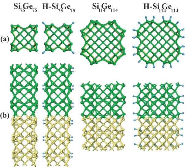
Figure 4.1: Optimized atomic structure of bare and hydrogenated SinGen
nanowire superlattices for n=75 and 114. a) Top view; b) Side view. Small-gray, large-light and large-dark balls correspond to the hydrogen, silicon and germanium atoms respectively.
CHAPTER 4. SINGEN NANOWIRE SUPERLATTICES 18
4.3
Bare and Hydrogenated Nanowires and
Nanowire Superlattices
In this study we considered bare and hydrogen passivated longitudinal SinGen
nanowire superlattices and also bare and hydrogen passivated Si and Ge nanowires as constituent structures. Bare Si and Ge nanowires are oriented along [001] direction of the parent diamond crystal and have normally N atoms in their primitive unit cell with lattice constant c along the nanowire (or z-) axis. We took N=25 and N=57 as two special prototypes. We designate them as SiNW(n) [GeNW(n)] or shortly Sin (Gen) with n=sN, s being an integer number. Sin and
SiN (Gen and GeN) indicates the same nanowire, except that the unit cell of the
former one includes s primitive cell in direct space with 1/s times reduced BZ in the momentum space. In our simulations bare Sin (Gen) nanowires are first cut
from the bulk crystal with ideal structural parameters. Subsequently ideal bare nanowires are relaxed to optimize their structure and lattice constant. Si (Ge) atoms near the core of relaxed nanowire has tetrahedral coordination. To obtain H-passivated Sin or Gen nanowires (designated as H-SiNW(n) or H-GeNW(n),
shortly as H-Sin or H-Gen) the dangling bonds at the surface are saturated by H
atoms and whole structure is re-optimized. Our study indicates that the atomic and electronic structure of H-Sin and H-Gen may depend on whether hydrogen
passivation and subsequent optimization are achieved on ideal or optimized bare Sin and Gen nanowires. The present sequence of structure optimization mimics
the actual growth of hydrogen passivated nanowires.
A SinGen has n=sN Si atoms at one side and n=sN Ge atoms at the other
side of NWSL unit cell. These atoms have tetrahedral coordination as if they are part of a SiGe heterostructure and hence at the interface Si atoms are bonded to Ge atoms pseudomorphically and make atomically flat interface. We note that pseudomorphic growth can sustain for small diameters; but misfit dislocations may be generated at the interface of large diameter (or large N) SinGen
super-lattice. Atomic positions and lattice constant are relaxed to obtain optimized structure. H-SinGen follow the same sequence of construction as H-Sin or H-Gen.
CHAPTER 4. SINGEN NANOWIRE SUPERLATTICES 19
and 75 are found to have c=10.9 ˚A, 21.8 ˚A and 32.7 ˚A, respectively. Upon hydrogenation these lattice constants change to c=11.2 ˚A, 22.3 ˚A and 33.5 ˚A, respectively. Lattice constants of bare and hydrogenated SinGen, n=57 and 114
are almost identical and are c=11.1 ˚A and 22.2 ˚A, respectively. Fig.4.1 shows the atomic structure of bare and hydrogen passivated SinGen for n=75 and 114.
These NWSLs are reminiscent of SinGen (001) planar superlattice which were
fabricated by molecular beam epitaxy by growing first n Si (001) plane and then
n Ge (001) plane, and eventually by repeating this SinGen(001) unit periodically.
While the SinGen (001) superlattice has 2D periodicity in (001) layers, NWSLs
under study here have finite cross section and hence 2D periodicity is absent. Electrons are bound to NWSL in radial (lateral) direction, but propagate as 1D Bloch states along the superlattice axis (in longitudinal direction).
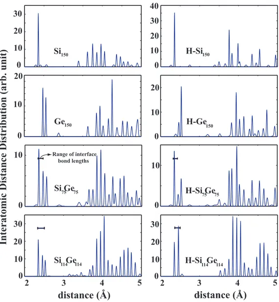
Interatomic distance distribution of Si75Ge75and H-Si75Ge75NWSLs are
com-pared with parent Si and Ge nanowires in Fig.4.2. In the same figure we also show the interatomic distance distribution of bare and hydrogenated Si114Ge114
NWSL. At the surface, optimized atomic structures of Sin and Gen deviate
con-siderably from the ideal structure of Sin and Gen. For example, one can deduce
quadrangles of atoms at the surface. Normally, NWSLs consist of hexagonal and pentagonal rings, where one can distinguish bond lengths in different categories. The interatomic distance distribution of SinGenis reminiscent of the sum of those
of Si2nand Ge2nexcept some changes originated from the interface between Si and
Ge segments of supercell. While bulk optimized Si-Si and Ge-Ge bond lengths are d=2.36 ˚A, and 2.50 ˚A, respectively, the Si-Ge bond at the interface ranges between 2.35 ˚A and 2.52 ˚A for bare Si228Ge228 (between 2.37 ˚A and 2.49 ˚A for
H-Si228Ge228). Nevertheless, the distribution exhibit several peaks corresponding
to the deviations from the bulk geometry at the surface. As the cross section or
N increases the effect of the surface decreases and the distribution of interatomic
CHAPTER 4. SINGEN NANOWIRE SUPERLATTICES 20 10 20 30 0 0 10 20 0 10 Si Ge
Interatomic Distance Distribution (arb. unit)
10 20 30 40 10 20 0 10 0
distance (A)
H-Si Ge75 75 75 75 0distance (A)
Ge150 Si150 H-Si150 H-Ge150 o o 10 0 20 30 Si Ge 10 20 30 H-Si Ge114 114 114 114 0 2 3 4 5 2 3 4 5 Range of interface bond lengthsFigure 4.2: Interatomic distance distribution of optimized bare and hydrogenated Si2n, Ge2n and SinGen for n=75 up to fourth nearest neighbor. The similar
distribution for Si114Ge114 and H-Si114Ge114 are also shown. The Si-H (Ge-H)
CHAPTER 4. SINGEN NANOWIRE SUPERLATTICES 21
4.4
Mechanical properties
The stability and elasto-mechanical properties of SinGen and H-SinGen NWSLs
are crucial for their possible use in nanoelectronics. In the present study the maximum diameter of nanowire we treated is ∼ 1.8 nm. The diameter of hy-drogenated Si25Ge25 NWSL is even smaller (∼ 1.4 nm). For such small diameter
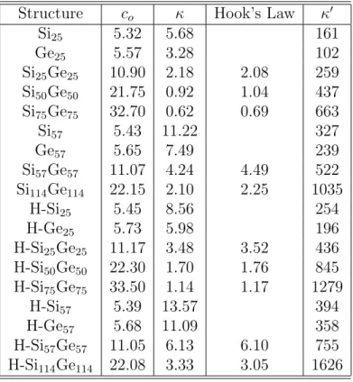
nanowires or NWSL’s, there are ambiguities in determining the area of cross sec-tion. Moreover, the surface to volume ratio is rather high and hence makes the cross section nonuniform. In view of these, the calculation of Young’s modulus may not be appropriate. Here we rather considered the force (spring) constants of nanowires and NWSLs under a strain in the harmonic region. To this end we calculated the second derivative of the total energy (per unit cell) with re-spect to the lattice constant c (i.e. κ=d2E
T/dc2) or to the strain, ²=∆c/c (i.e.
κ0=d2E
T/d²2). The values calculated for nanowires and NWSLs treated in our
paper are given in Table 4.1.
Like bulk crystals, Sin nanowires are stiffer than Gen nanowires. This implies
that the lattice mismatch between Si and Ge nanowires in NWSL is accommo-dated mainly by the Ge zone. For both nanowires and NWSL, κ increases with increasing cross section. For example κ of Si25 is almost the half of κ of Si57.
Note that κ(Si50) ' κ(Si25)/2. As for, κ of Si25Ge25 NWSL calculated from first
principles is 2.18 eV/˚A. This value can be estimated in terms of two springs con-nected in series, namely κ−1(Si
25Ge25) ' κ−1(Si25)+κ−1(Ge25) to be κ(Si25Ge25)
' 2.08 eV/˚A. We, therefore, conclude that as long as the geometry and size of the cross section remained to be similar, classical Hook’s law continues to be ap-proximately valid even for nanostructures. Upon hydrogenation both nanowires as well as NWSLs studied here become stiffer. The spring constant of Si57Ge57
is twice that of Si114Ge114, because the latter NWSL has twice the length of the
former. We also calculated the ratio of the strain of the Ge-zone to that of Si-zone of Si75Ge75 under tensile stress, i.e. ² (Ge)/² (Si) to be ∼ 2.5. These calculations
have been performed by minimizing the total energy under a preset uniaxial strain in the elastic range. The strain on Ge and Si-zone calculated are determined after full relaxation. The ratio found is reduced to ∼ 1.25 for Si114Ge114. In compliance
CHAPTER 4. SINGEN NANOWIRE SUPERLATTICES 22
Table 4.1: Equilibrium values of lattice parameter c are given in units of ˚A. Force constant κ (as defined in the text), in units of eV/˚A, is calculated by using both VASP result and Hook’s law. Percentage difference in between force constant values calculated from VASP result and Hook’s law is given within parenthesis in order to check whether classical Hook’s law is still valid in nanoscale. Also force constant κ0 (as defined in the text) is presented in units of eV.
Structure co κ Hook’s Law κ0
Si25 5.32 5.68 161 Ge25 5.57 3.28 102 Si25Ge25 10.90 2.18 2.08 259 Si50Ge50 21.75 0.92 1.04 437 Si75Ge75 32.70 0.62 0.69 663 Si57 5.43 11.22 327 Ge57 5.65 7.49 239 Si57Ge57 11.07 4.24 4.49 522 Si114Ge114 22.15 2.10 2.25 1035 H-Si25 5.45 8.56 254 H-Ge25 5.73 5.98 196 H-Si25Ge25 11.17 3.48 3.52 436 H-Si50Ge50 22.30 1.70 1.76 845 H-Si75Ge75 33.50 1.14 1.17 1279 H-Si57 5.39 13.57 394 H-Ge57 5.68 11.09 358 H-Si57Ge57 11.05 6.13 6.10 755 H-Si114Ge114 22.08 3.33 3.05 1626
with the κ values in Table 4.1, this result indicates that in a SinGen NWSL Ge
zone elongates more than Si-zone. Using empirical potential, Menon et al. [39] were able to calculate the Young’s modulus and bending stiffness of tetrahedral and cage-like Si nanowire of ∼ 4 nm diameter, and found values comparable with bulk values.
CHAPTER 4. SINGEN NANOWIRE SUPERLATTICES 23
Band Energy (eV)
Band Energy (eV)
Si
150Ge
150Si
75Ge
75H-Si
150H-Ge
150H-Si
75Ge
750 1 -1 0.5 0 -0.5 Γ kz Z Γ kz Z Γ kz Z
Figure 4.3: Energy band structures of optimized bare and hydrogenated Si2n,
Ge2n nanowires and SinGen nanowire superlattices for n=75. Zero of energy is
taken at the Fermi level. Band gaps are shown by shaded zones. Dashed and dotted lines (minibands) are obtained by folding of Si50 (also H-Si50) and Ge50
CHAPTER 4. SINGEN NANOWIRE SUPERLATTICES 24
Si
228Ge
228Si
114Ge
114H-Si
228H-Ge
228H-Si
114Ge
114Band Energy (eV)
Band Energy (eV)
0 1 -1 0.5 0 -0.5 Γ kz Z Γ kz Z Γ kz Z
Figure 4.4: Energy band structures of optimized bare and hydrogenated Si2n,
Ge2n nanowires and SinGen nanowire superlattices for n=114. Zero of energy is
taken at the Fermi level. Dashed and dotted lines are obtained by folding of Si57
CHAPTER 4. SINGEN NANOWIRE SUPERLATTICES 25
4.5
Electronic Properties
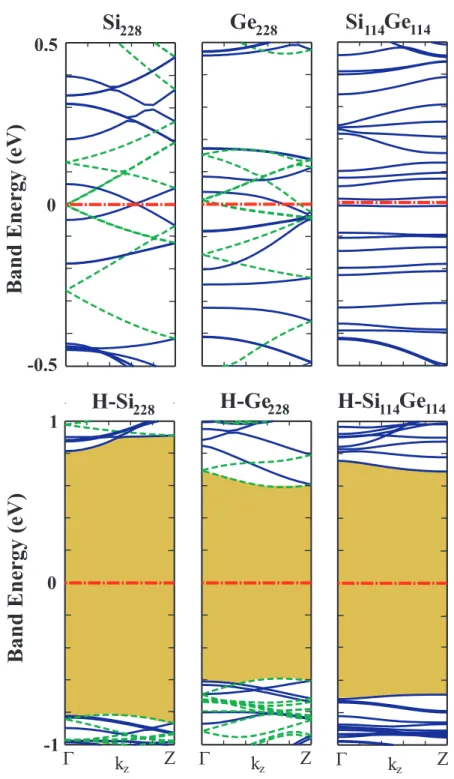
The band structures of optimized bare and hydrogenated SinGen are given in
Fig.4.3 and Fig.4.4 for n=75 and 114, respectively. In the same figures the band structures of bare and hydrogenated Si2n and Ge2n constituent nanowires are
presented for the sake of comparison. SiN (N=25 and 57) and hence any Si2n
(n=sN) nanowires are metallic due to the surface dangling bonds. Similarly GeN
(N=25 and 57) and hence any Ge2n are metallic. Upon passivation of dangling
bonds, these metallic nanowires become semiconductor. For example, H-Si150and
H-Ge150 nanowires have indirect band gaps, Eg=1.1 eV and 0.7 eV, respectively.
Normally, the band gap of a H-Sin is inversely proportional to its diameter, if the
corresponding ideal nanowire cut from the bulk crystal were directly passivated with H before the structural optimization. Also the band gap is affected by the cross section geometry for small N. For large N, the variation of Eg with N is
more uniform.
Like Si150 and Ge150, Si75Ge75 is metallic. The ideal equilibrium ballistic
conductance of Si150, Ge150nanowires and Si75Ge75NWSL is revealed to be 6e2/h,
10e2/h and 8e2/h, respectively. Since H-Si
150 and H-Ge150 are semiconductors,
H-Si75Ge75 NWSL is also semiconductor: Its band gap is 0.7 eV and close to the
band gap of H-Ge150. H-Si114Ge114 has a direct band gap of 1.4 eV. Again it is
smaller than the band gap of H-Si228, but closer to that of H-Ge228.
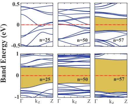
In Fig.4.5 we examine how the electronic energy bands of nanowire superlat-tices evolve with the lattice constant c or s. In the case of N=25, bare SinGen
nanowire superlattices are metallic for all n (n=25, 50 or s=1, 2 and 3). As s increases additional minibands occur and they become flatter. As for H-SinGen’s,
they are all semiconductor for n=25, 50 and 75. As n increases all bands including lowest conduction and highest valence band become flatter with the formation of minibands. In this respect, the band gap becomes more uniform as s increases. Similar behaviors are displayed also for H-SinGenwith n=57 and 114 (see Fig.4.4).
Unexpectedly, bare SinGen’s are semiconducting for n=57 and 114. The band gap
decreases from 0.27 eV to 0.02 eV as s increases from 1 to 2. Isosurface charge densities of these states near the band gap edges found that they are confined in
CHAPTER 4. SINGEN NANOWIRE SUPERLATTICES 26
0
-0.5
0.5
n=25 n=50 Γ kz Z Γ kz ZBand Energy (eV)
n=25 n=501
-1
0
Γ kz Z n=57 n=57Figure 4.5: Energy band structure of bare and hydrogenated SinGen nanowire
superlattices for n=25, 50 and 57.
one of the zones. It is concluded that opening of the band gap originates from the mismatch of surface dangling bond states in Si and Ge zones.
It should be noted that the band gap is underestimated by the GGA calcula-tions used in the present study. GW correccalcula-tions performed recently [40] for H-Sin
in different orientation is in the range of 0.5-0.6 eV for large diameters. In view of the fact that Ge bulk is predicted as metal by GGA calculation, GW correc-tion for H-Gen nanowires is expected to be in the same range as that for H-Sin.
Under this circumstances a scissor operation (namely increasing the band gap of corresponding SinGen by the same amount 0.5-0.6 eV) may yield the actual band
gap. In summary, the band gaps of H-SinGen predicted by GGA calculation are
CHAPTER 4. SINGEN NANOWIRE SUPERLATTICES 27
0
Band Energy (eV)
0.5
-0.5
Γ
k
zZ
QW
Si
Ge
H-Si
75Ge
75BAND GAP DIAGRAM
c
sc
Figure 4.6: Schematic description of energy band diagram in the unit cell (on the right and upper side), band structure in momentum space (on the left side) and isosurface charge density of states of H-Si75Ge75 NWSL at the band edges.
CHAPTER 4. SINGEN NANOWIRE SUPERLATTICES 28
H-Si
114Ge
114Γ
k
zBand Energy (eV)
0
1
-1
Z
Si
Ge
BAND GAP DIAGRAM
c
sc
QW
Figure 4.7: Schematic description of energy band diagram in the unit cell (on the right and upper side),band structure in the momentum space (on the left side) isosurface charge density of states of H-Si114Ge114 NWSL at the band edges.
CHAPTER 4. SINGEN NANOWIRE SUPERLATTICES 29
4.6
Confined states
The results discussed in the previous section reveals that Sin and Gen nanowires
making a Si/Ge heterojunction in the supercell have band gaps of different width. Upon a pseudomorphic junction the bands and hence band gaps corresponding to Si and Ge zones are aligned. Combination of two features, namely Si and Ge zones having different band gaps and band-lineup result in band discontinuities and hence band-offsets. The conduction and valence band edges of different zones (Si-zone or Ge-zone) in the nanowire superlattice will have different energies. Under these circumstances, the diagram of the conduction band edge along the axis of NWSL will display a multiple quantum well structure with the periodicity of csc like a Kronig-Penny model. Electrons in the well region of a zone should
decay in the adjacent zones having higher conduction band edge, since their energy will fall into the band gap of this barrier zone. As a result, the states of these confined (or localized) electrons are propagating in the well, but decaying in the barrier. Usually, confined electrons have low group velocity. They may become more localized if the barrier is high and the width of barrier is large. If the confinement (or localization) is complete, electrons in adjacent levels do not interact and the associated band En(kz) becomes flat. Accordingly, such a state
has RwellΨ∗
cΨc−→dr À
R
barrierΨ∗cΨc−→dr. This is known as Mott localization. Similar
arguments are valid for the hole states if the energies of valence band edges of both zones are different.
In the past, the reference energies in determining band-offsets of 2D superlat-tices have been actively studied both experimentally and theoretically. Energy diagram of conduction and valence band edges are then used as effective po-tential forming a multiple quantum well structure.[41] The states of conduction band electrons and holes of valence band were treated using Effective Mass The-ory (EMT). These states are free electron-like 2D bands in the planes and Bloch states forming minibands perpendicular to the planes. The conditions are, how-ever, different in NWSLs. First of all, EMT may not be applicable directly in the present case, in particular for NWSLs with small diameter. Secondly, the ref-erence energy level determined for planar superlattices may not be appropriate.
CHAPTER 4. SINGEN NANOWIRE SUPERLATTICES 30
Recently, Kagimura et al. [28] proposed surface dangling bond states as reference level for Si/Ge core-shell superlattices. Under estimation of band gaps by DFT GGA calculation may hinder the accurate determination of band-lineups. Voon and Willatzen [29] draw attention to the lateral confinement of states in NWSL’s. Using one-band EMT and by solving Ben Daniel-Duke [42] equation they found that the effective barrier is lowered due to the coupling between radial and longi-tudinal confinement. In particular, they predicted, that the effective barrier and hence confinement disappears below a critical radius of ∼ 5 nm. In the present study, the maximum radius of NWSL was ∼ 0.9 ˚A which is much lower than the critical radius set for GaAs/AlGaAs NWSLs.[29]
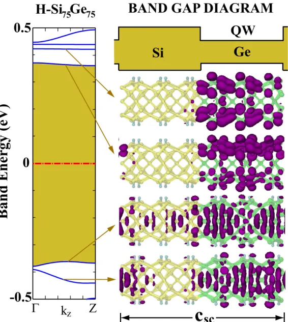
In the present study we examined whether some of states can be longitudinally confined, by performing an extensive analysis of charge densities of superlattice bands calculated by first-principle methods. The formation of periodic quantum well structure is schematically described in Fig.4.6. We expect that the values of band gaps in the H-Si and H-Ge zones in a unit cell of the H-Si75Ge75 cannot
deviate significantly from the values calculated for periodic H-Si25 and H-Ge25
nanowires (namely, 1.1 eV and 0.7 eV, respectively). When the two zones are connected by an atomically flat interface, H-Ge zone can form a well between adjacent H-Si zones, since the band gap of the former zone is smaller and the energy of conduction band edge is lower relative to that of the latter zone. Upon normal band-lineup, H-Ge75 zone acts as a quantum well for both lowest
conduc-tion and highest valence band electrons. Band structure of H-Si75Ge75 with two
lowest conduction and two highest valence minibands and their isosurface charge distribution in the superlattice unit cell are shown in Fig.4.6. The distribution of electronic charge density is confirming the above normal band-lineup. Both conduction band states are confined in the H-Ge75zone, but they have very small
weight in the H-Si75 zone. Similarly, states corresponding to two highest valence
bands are also confined in the H-Ge75 zone. It should be noted that owing to the
charge transfer between adjacent zone the form of the energy band diagram may change from the simple form given in Fig.4.6.
In Fig.4.7 we present similar analysis for H-Si114Ge114 NWSL. As compared to
CHAPTER 4. SINGEN NANOWIRE SUPERLATTICES 31
minibands owing to larger number of Si and Ge atoms. The ways the highest valence band and the lowest conduction band states are confined in different zones suggest a staggered band line-up. Highest valence band states are confined in the H-Ge zone; but lowest conduction band states are confined in H-Si zone. States of 6th and 7th valence band (from the top) are propagating throughout the NWSL.
We believe that present ab-initio results revealing confined states for NWSLs with a radius as small as ∼ 0.6 nm are not contradicting the conclusions obtained from one-band EMT model. We think EMT as applied in Ref. 7 has to be revised for small diameter NWSL. Moreover, the material parameters of GaAs/AlGaAs relevant for EMT by themselves are different from SinGen nanowire superlattices
studied here. We also note that H-SinGen nanowire superlattice has 1D rodlike
structure. There are several minibands in the 1D BZ. Number of minibands in a given energy interval increases with either increasing N (i.e. increasing diameter) or increasing s. A nanowire superlattice with a long unit cell having several Si or Ge atoms will have several (quasi continuous) minibands. States of H-Sin or
H-Gen zone of the same energy are more likely to match each other to construct
a state that propagate throughout the NWSL. Otherwise, a superlattice of small radius with short unit cell have small number of bands. Then the states in different zones are less likely to match. A state, which cannot find a matching partner is confined to its zone. As a matter of fact, we were able to deduce confined states even in the barrier zone (H-Si) with energies higher than the conduction band edge.
Chapter 5
Size Modulated Si NWSL
Rod-like Si nanowires (SiNW) have been synthesized down to ∼ 1 nm diameter.[11] They are attractive one-dimensional (1D) materials because of the well-known silicon fabrication technology that make them directly usable on the Si-based chips. Even if unsaturated dangling bonds on the outer surface usually attribute a metallic character to SiNWs, they become insulator (or semiconduc-tor) upon saturation of these dangling bonds by hydrogen atoms.[43] SiNWs display diversity of electronic properties depending on their diameter, as well as their orientation. In particular, the band gap of semiconductor SiNWs varies with their diameters. They can be used in various electronic, spintronic and optical applications, such as field effect transistors [44], light emitting diodes [45], lasers [46] and interconnects. The conductance of these semiconductor nanowires can be tuned easily by doping[47, 48] during the fabrication process or by applying a gate voltage. Recent studies have shown that 3d transition metal doped Si nanowires become half-metallic.[49]
5.1
Calculations and Results
This part of the thesis demonstrates that SiNWs of different diameters can form stable superlattices. The electronic band structure of the superlatice is different
CHAPTER 5. SIZE MODULATED SI NWSL 33
from the constituent SiNWs and is modulated in real space leading to a multiple quantum structure and/or to a series of quantum dots. In these size induced quantum wells, specific states are confined. These results are obtained by per-forming first-principles plane wave calculations within Density Functional Theory (DFT)[34] using ultrasoft pseudopotentials.[35, 33] The exchange correlation po-tential has been approximated by GGA using PW91 functional.[36] All structures have been treated within supercell geometry using the periodic boundary condi-tions. A plane-wave basis set with kinetic energy cutoff of up to 250 eV has been used. In the self-consistent potential and total energy calculations the Brillouin zone is sampled in k-space within Monkhorst-Pack scheme[38] by (1×1×11) mesh points for the smallest structure. This sampling is scaled according to the size of superlattices. All atomic positions and lattice constants are optimized by using the conjugate gradient method where total energy and atomic forces are mini-mized. The convergence for energy is chosen as 10−5 eV between two steps, and
the maximum force allowed on each atom is 0.02 eV ˚A.
Here Si nanowires (i.e. SiN1 with diameter ∼ D1 and having N1 Si atoms
in the primitive unit cell) is first cut from the ideal bulk crystal along desired direction. Then in every alternating segment comprising l1 unit cell the diameter
D1 is kept fixed, but in the adjacent segment comprising l2 unit cell (each having
N2 Si atoms) the diameter is reduced to D2. The latter part can be identified
as the segment of SiN2 nanowire. At the end, the segments of SiN1 and SiN2
have made a smooth junction and hence formed an ideal superlattice SiN so that
its diameter is modulated in real space. Note that N ≤ l1N1 + l2N2, because
some surface atoms attaching with a single bond to the surface were removed at the beginning. Subsequently we relaxed the atomic structure of bare and ideal SiN. Upon relaxation, the dangling bonds on the surface are saturated by H
atoms and SiNHM superlattice is further relaxed for final atomic structure. This
superlattice can be described by a rod with alternating diameters or a nanowire with alternating wide and narrow parts.
We consider two superlattice structures, namely Si138H42 and Si157H64, which
are grown in [111] and [100] directions, respectively. For the latter we investigate the surface defect and also Al and P substitutional impurities. The superlattice
CHAPTER 5. SIZE MODULATED SI NWSL 34
ENERGY
(eV)
1
-1
0
0.5
-0.5
Γ
k
zΖ
Si
138H
42BAND
CHARGE DENSITY ISOSURFACES
[111]
2
1Figure 5.1: Energy band structure and charge density isosurfaces of the super-lattice, Si138H42, formed from periodically repeated junctions consisting of one
unit cell of SiNW with D1 ∼ 11 ˚A and two unit cell of SiNW with D2 ∼ 7
˚
A formed along [111] direction. Isosurfaces of charge density of valence and con-duction band states confined at different regions in real space. Large and small balls indicate Si and H atoms. Zero of energy is set at the Fermi level shown by dash-dotted line.
CHAPTER 5. SIZE MODULATED SI NWSL 35
Si138H42 is formed by the junction of the segments Si38H12 and Si68H18 with
seg-ment lengths of l1 = 1 and l2 = 2. Normally, states can propagate along the
axis of the superlattice and form dispersive bands. Whereas some states can be confined to either narrow or wider parts of superlattice, if they cannot find a matching state in the adjacent part. Stated differently, if the energy of a particu-lar state in the narrow or wide part falls in the band gap of the adjacent part, it becomes confined. Energy bands and isosurface charge density of states in specific bands are shown in Fig. 5.1. One sees propagating states, which have charge den-sity distributed everywhere in the superlattice rod as well as states, which have high charge density in the alternating (either wide or narrow) segments. The lat-ter types of states are identified as confined states. Defining the confinement as
R
l1,2|Ψ(r)|
2dr, the longer the lengths of different segments, l
1 and l2, the stronger
becomes the confinement. For example, if a state is confined to the segment l1, its
confinement increases with increasing l2, since the spill over of the confined state
into the segment l2 decreases. For perfect localization, where coupling between
confined states are hindered, the segment l1 behaves as a quantum dot.
Con-finement and band edge alignment in the present superlattice are reminicent of the 2D pseudomorphic or commensurate semiconductor superlattices.[41] While the states of flat degenerate band at the top of the valence band are confined in the narrow segment of the superlattice, the state at the conduction band edge is confined at the wide segment. This situation implies the staggered band align-ment with confined hole states in the narrow part and confined electrons in the wide part. A state near ∼ -1 eV is a propagating state. Owing to short superlat-tice periodicity, a non-negligible coupling between confined states result in bands which exhibit minute dispersion.
Figure 5.2(a) presents the superlattice formation and confined states in a dif-ferent structure, namely Si157H64 with l1 = 2, l2 = 3 and D1 ∼ 14 ˚A, D2 ∼ 7
˚
A formed along [100] direction. Flat minibands near the edge of conduction and valence bands are distinguished. In contrast to propagating states of dispersive bands near 1 eV, the states of these flat mini bands are confined in the narrow seg-ments of the superlattice. This situation indicates normal band lineup. We note
CHAPTER 5. SIZE MODULATED SI NWSL 36
ENERGY
(eV)
1
-1
0
0.5
-0.5
Γ
k
zΖ
Si
157H
64BAND CHARGE DENSITY ISOSURFACES
[100]
E
FE
defecta)
b)
ar
b
. u
n
its
wide
interface
narrow
Distance(A)
o2
4
2
4
2
4
INTERATOMIC DISTANCE DISTRIBUTION
Figure 5.2: (a) Same as Fig. 5.1 for Si157H64 formed from periodically repeated
junctions consisting of two unit cell of SiNW with D1 ∼ 14 ˚A and three unit
cell of SiNW with D2 ∼ 7 ˚A formed along [100] direction. The charge density
isosurfaces of the defect state (due to one Si and one H atom attached to it is missing from Si157H64) and the state below corresponding to the structure Si156H63
is shown in the dashed box. (b) The distribution of interatomic distances of relaxed superlattice. The arrows indicate the ideal bulk 1st, 2nd and 3rd nearest neighbor distances.

![Figure 2.2: STM images of silicon nanowires grown along [112] and [110] direc- direc-tions, as given in the Ref](https://thumb-eu.123doks.com/thumbv2/9libnet/6021100.127128/19.892.178.780.173.418/figure-images-silicon-nanowires-grown-direc-direc-tions.webp)