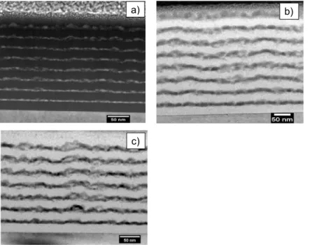
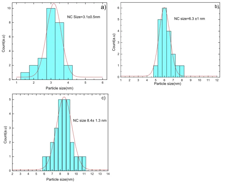
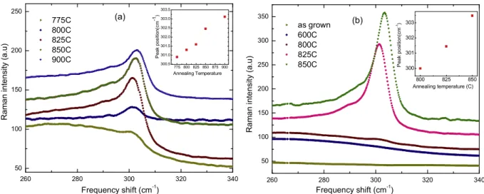
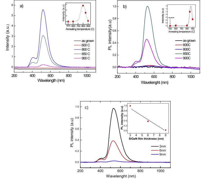
Ge nanocrystals embedded in ultrathin Si3N4 multilayers with SiO2 barriers
Tam metin
Şekil
Benzer Belgeler
Stöl 3 Les jeux verbaux, pris au sens très large, englobent, d’un côté, les jeux avec les mots, une fin en soi visant uniquement à faire montre d’un maniement habile du
The performances of the estimators of Candan, Quinn, Macleod, Jacobsen and the Cramer-Rao bound for frequency estimation variance (given by (4.1)) are compared
A weighted superposition of 3D plane waves over a continuum of propa- gation angles for the monochromatic case, in the form of in- tegrals as presented, yields the 3D field;
In their analysis, they employed Hotelling’s original model with locations and prices variable, a linear market of length ℓ, and a uniform demand, but their model included
Aims: The aim of this study was to evaluate the radiological and clinical results of a single-stage surgical treatment with locking compression plates (LCPs) and autologous
Given the above variants regarding optimal product positioning in STP problems, we propose a clusterwise multidimensional unfolding procedure that simultaneously identifies segments
The holograms of the micro-lenses are recorded in the near infrared by means of digital holographic microscopy as image -plane holograms whereas the holographic
Kudryashov’un yedinci mertebeden lineer olmayan diferansiyel denklemlerin analitik çözümlerini elde etmek için geliştirmiş olduğu Kudryashov metodu [27] modifiye edilerek
