ELSEVIER Surface Science 323 (1995) 295-303
i~iiiiiiiiiii~iii~i~iii~ii~ii~iiiiiii~iii~!ii!~iii~iiiii~i~i~iii!~ii!~iiii~i!iiiiiii~
s u r f a c e s c i e n c e
Initial stages of SiGe epitaxy on Si(001) studied by scanning
tunneling microscopy
A. Oral *'1, R. Ellialtioglu
Department of Physics, Bilkent University, 06533 Ankara, Turkey Received 18 August 1994; accepted for publication 7 October 1994
Abstract
We have studied the initial stages of strained SiGe alloy growth on the Si(001)-(2 × 1) surface by scanning tunneling microscopy. The Si0.36Ge0.64 alloy was grown on the silicon substrate at various coverages (0.13-3.6 ML) and at different temperatures ( ~ 310-470°C). The growth was one dimensional, preferring the direction perpendicular to the underlying silicon dimer rows at low coverages and low temperatures. Anti-phase boundaries were observed to lead multi-layer growth. Strong interaction between the overlayer and the substrate was found to buckle the substrate as well as SiGe dimers. Different growth mechanisms, island formation and step flow, were identified at low and high substrate temperatures. (2 X n) ordering of the strained overlayer was only observed at an intermediate growth temperature ( ~ 390°C).
Keywords: Epitaxy; Scanning tunneling microscopy; Silicon; Silicon-germanium
I. I n t r o d u c t i o n
The epitaxial growth of Sil_xGe x alloy on silicon substrates by using molecular beam epitaxy (MBE) and chemical vapour deposition (CVD) has become a very important issue over the last few years. Si and Ge form solid solutions at almost all compositions. Since the lattice constant of bulk Ge is 4.3% larger than Si, SiGe alloys grown on Si substrates are strained. However, the strain is relaxed if the thick- ness of the grown layer exceeds the critical thickness
* Corresponding author.
1 Present address: School of Physics, University of Bath, Claverton Down, B A 2 7AY, Bath, UK. E-mail: [email protected].
which depends on the concentration. Growth of this technologically as well as scientifically important alloy has been extensively studied by various groups using different techniques [1-5]. This material sys- tem has attracted much attention for the potential opto-electronic applications [6]. Very high electron mobilities and the fractional quantum Hall effect have been observed in the strained Si layers grown between relaxed SiGe layers [7-9]. Ordering of the Si and Ge atoms within the alloy has been predicted [10], observed by various groups [3-5] and it is still subject of controversy [11]. Since the SiGe alloy system is compatible with the existing silicon micro- fabrication technology, it represents a challenging alternative to I I I - V semiconductor based device technology and recently, high speed commercial ap- plications have started to emerge from SiGe based devices [12].
0039-6028/95/$09.50 © 1995 Elsevier Science B.V. All rights reserved SSDI 0 0 3 9 - 6 0 2 8 ( 9 4 ) 0 0 6 6 6 - 0
296 A. Oral, R. Ellialtioglu / Surface Science 323 (1995) 295-303 Recently silicon homoepitaxy on Si(001) [13-15]
and germanium heteroepitaxy on Si(001) [13,16,17] have been investigated in detail using scanning tun- neling microscopy (STM) by various groups. These experiments lead to better understanding of surface diffusion and epitaxial growth at the atomic scale. Although epitaxial growth of Sit_xGe x on Si has been extensively studied, the early stages of Si I _ xGe x growth on Si(001) at the atomic level is still not well understood.
In this work we have analysed the initial stages of SiGe epitaxial growth on the Si(001) surface as a function of coverage and temperature using scanning tunneling microscopy (STM) for the first time. We have observed that the alloy grows pseudomorphi- cally by island formation at low substrate tempera- ture, T~ = 310°C. The step flow mechanism takes over at high growth temperature, T~ = 470°C. How- ever, at an intermediate growth temperature of T s = 390°C, the alloy has been observed to be growing partially relaxed by 2 X n ordering of the overlayer.
2. Experimental details
The experiments were performed in a ultra high vacuum (UHV) system with a base pressure of < 3 X 10 - 1 ° Torr. The UHV system has been built in our laboratory [18] and is equipped with STM, Auger
electron spectroscopy (AES), low-energy electron diffraction (LEED) for surface analysis, an e-beam heater and Si and Ge evaporation sources for the sample preparation. A fast-entry load-lock chamber allows easy exchange of tips and samples. The STM used in this study was a home-made instrument with a single tube scanner and a two-axis stick-slip coarse positioner, which is described in detail elsewhere [19]. 6 X 8 mm Si(001) samples were cut from com- mercially available [20] 525/xm thick, n-type wafers with 1-10 ~ . cm resistivity and misoriented 0.5 ° towards the [110] direction. This vicinal angle gives
o
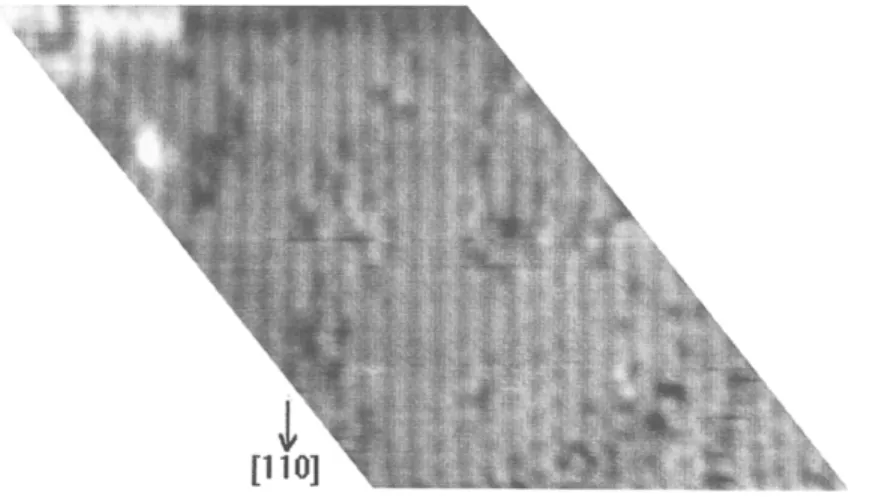
an average terrace size of around 160 A, which was confirmed by the STM results. The Si(001) samples were first degreased and cleaned with a wet-chem- ical oxide etch-regrowth procedure [21] and mounted on degassed tantalum sample holders before intro- ducing them into the UHV chamber. The samples were degassed in the UHV for approximately 10 h at 680°C by using an e-beam heater. An atomically flat, (2 X 1) reconstructed Si(001) surface was ob- tained after heating the sample briefly to ~ 900°C in situ to remove the final oxide layer. This procedure routinely gave well ordered and contamination-free Si(001)(2 X 1) surfaces as observed by LEED, STM and AES. Fig. 1 shows a high resolution STM image of a typical Si(001)(2 x 1) surface prepared by this recipe. The clean Si(001) surface has a small number of defects and most of the dimers are observed to be symmetric. It is well known that even an extremely
A, Oral, R. Ellialtioglu / Surface Science 323 (1995) 295-303 297
//
a [ I *',i
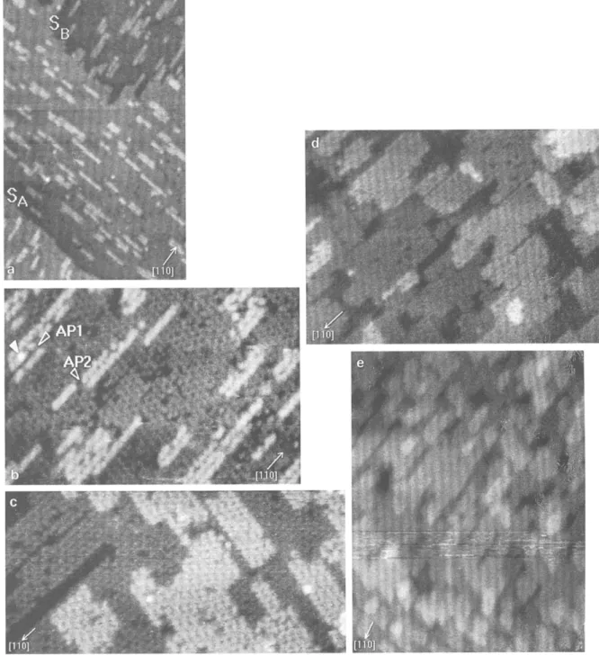
Fig. 2. Epitaxial growth of 5i0.36Ge0.64 on Si(001) at T s = 310°C observed by STM. Coverages: (a) 0.13, (b) 0.25, (c) 0.8, (d) 1.6, and (e) 3.5 ML. Images sizes: (a) ~ 640 X 1000, (b) ~ 340 × 230, (c) ~ 390 X 185, (d) ~ 490 X 340, and (e) ~ 770 x 960 ,~. The S A and S a type steps are shown in (a). Antiphase boundaries, AP1 and AP2 are displayed in (b). The multilayer growth around AP1 is marked by a triangle on (b).
298
A. Oral, R. Ellialtioglu / Surface Science 323 (1995) 295-303 low amount of some impurity like Ni, causes a(2 × n), n = 8, reconstruction on the Si(001)(2 X 1) surface. We have never observed the influence of such impurities on Si(001) substrates cleaned with our recipe, which would have also affected the SiGe epitaxy.
Silicon and germanium were evaporated from separate home-made sources, which were composed of directly heated pieces of Si wafer and germanium granules held in tungsten baskets. The sources were water-cooled in order to reduce the outgassing of that part of the chamber. The evaporation rates of the silicon and germanium sources were calibrated using the STM itself by counting the islands grown on the Si(001) surface. Rate calibration was carried out at a low substrate temperature, T s = 200°C, to minimise the number of atoms incorporating into the steps. The concentration of the alloy was then calculated using the evaporation rates of the silicon and germa- nium sources. The
Si0.36Ge0.64
alloys were grown on Si(001)(2 X 1) substrates at various coverages and at different temperatures. This alloy composition has been chosen randomly. The effect of alloy composi- tion on the structure of the epitaxial layer will be the subject of a further study. The growth rate was kept fixed at 0.2 M L / m i n throughout the experiments and different5i0.36Ge0.64
coverages were obtained by increasing the exposure time of the sample. A new sample was used for each experiment.An infrared pyrometer was used for temperature measurement in the high temperature range. In addi- tion, a K-type thermocouple mounted at the center of a Si sample was used to calibrate the heater at low temperatures and the heater input power was then used to deduce the substrate temperatures. Samples as well as sample holders used in the experiments were of the same size in order to achieve tempera- ture reproducibility. Tungsten tips prepared from a 0.2 mm diameter wire by electrochemical etching in KOH solution floated on CCI 4 were degreased and used without any further in situ treatment. These tips were used as long as they gave atomic resolution. STM images presented in this work were recorded with a negative sample bias of 2 V, thus imaging the filled sample states. The empty state imaging was rarely used throughout our experiments. Tunneling currents between 0.25 and 1 nA were used through- out the experiments.
3. Results
Fig. 2 shows the STM images of
5i0.36Ge0.64
grown on Si(001) samples at various coverages from 0.13 to 3.5 ML. These samples were grown at a relatively low substrate temperature of 310°C. At very low coverage, 0 = 0.13 ML, the growth was highly anisotropic as shown in Fig. 2a and the alloy grew almost as one dimer wide " s t r i n g s " oriented perpendicular to the underlying Si dimer rows. The dimerization direction of the grown layer is not surprising, because the successive layers of the Si(001) are reconstructed orthogonal to each other. Isolated dimers, as well as wider islands were also observed to have grown on the substrate. The same behaviour was also observed in our evaporation source calibration experiments, Si on Si(001) and Ge on Si(001). This anisotropy arises due to a sticking coefficient which is much larger at the end of the dimer rows than along the dimer rows [13]. Further- more, the formation energy of S A type steps is lower than that of S B type [22] and the anisotropic growth of the islands perpendicular to the underlying Si(001) dimer rows is also thermodynamically preferred. Dif- fusion of a Si or a Ge atom along the substrate dimer rows on the surface is much easier than in the perpendicular direction [23]. However, this cannot suppress the observed anisotropy since the diffusion along the steps and the sticking coefficient at the end of the dimer rows are also high and the migrating atoms prefer to incorporate at the end of the dimer rows. Moreover, the S A type steps were observed to be better sinks for the evaporated Si and Ge atoms migrating on the lower terrace compared to the ones on the upper terrace, as can be seen from uneven denuded zones around these steps in Fig. 2a. How- ever, S B type steps were equivalent sinks for the atoms migrating on both of the terraces, because the denuded zones around these steps were almost equal [13].The shape anisotropy was reduced and wider islands perpendicular to the dimer rows began to grow as the coverage was increased to 0 = 0.26 ML as shown in Fig. 2b. The formation of antiphase boundaries can be observed even at this coverage when two islands meet and if the dimers in these neighbouring islands were out of phase by one unit cell of the unreconstructed Si substrate. There were
A. Oral, R. Ellialtioglu / Surface Science 323 (1995) 295-303 299
two types of antiphase boundaries (AP) on the over- layer. AP1 forms when two different phase islands meet along the dimer rows as can be seen in Fig. 2b.
On the other hand, AP2 is formed if those islands met at the end of the dimer rows. Multilayer growth of the alloy has been observed to be promoted by
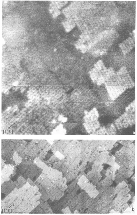
Fig. 3. Growth of 5i0.36Ge0.64 on Si(001) at /~ = 390°C observed by STM. Film thicknesses: (a) 0.5, and (b) 3.5 ML. Fields of view : (a) ~ 390 × 390, and (b) ~ 815 × 450 ,~.
300 A. Oral, R. Ellialtioglu / Surface Science 323 (1995) 295-303
these antiphase boundaries as pointed out in Fig. 2b. Another interesting feature was the complete buck- ling of the silicon substrate dimers as can be seen in Figs. 2b and 2c. This leads to change in the recon- struction from (2 X 1) symmetric to c(4 X 2) anti-
symmetric (buckled) configuration [17]. Moreover, the dimer structure of the epitaxial alloy is symmet- ric if the islands are one dimer wide and buckled otherwise [14].
The energy difference between the symmetric and
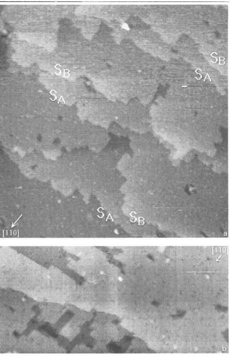
Fig. 4. S T M image of (a) 0.8 M L and (b) 3.5 M L Sio.36Geo.64 grown on Si(001) at ~ = 470°C. Images sizes : (a) ~ 1950 × 1950, and (b) ~ 725 X 340 A. The S A and S B type steps are marked in (a).
A. Oral, R. Ellialtioglu / Surface Science 323 (1995) 295-303 301 the buckled dimers on the Si(001) surface is very
small, and either defects, thermal excitations [24] or tip-sample interactions affect the appearance of the dimers [25]. In this work, the compressive strain in the alloy was partially transmitted to the substrate and this interaction increases the energy difference between two equivalent configurations of the buck- led dimers on the substrate such that it can no longer be suppressed by tip-sample interactions or thermal excitations. It should be pointed out that even though the strain in the
5io.36Geo.64
should be substantially lower than for epitaxial Ge on Si(001) [17], it is still sufficient to buckle the silicon substrate dimers com- pletely.Further growth of the SiGe alloy resulted in the merging of the 2D islands with themselves and with the substrate steps. Fig. 2c shows the STM image of 0.8 ML
Sio.36Geo.64
grown on Si(001) under the same experimental conditions. The second epitaxial layer has started to grow before the first layer was completed. Another interesting observation was the lack of (2 x n), n > 8, reconstruction on the over- layer grown at this temperature. (2 × n) reconstruc- tion of the thick Sio.sGe0. 5 layers grown on Si(001) by MBE has been observed by Butz and Kempers [26].When the coverage was increased to 0 = 1.6 ML, the first overlayer was still not complete, as shown in Fig. 2d. The SiGe islands just met one another and merged on the substrate and then combined with the substrate steps. Even the third layer has started to grow at the expense of the first and the second layers. At this low growth temperature, T~ = 310°C, the number of antiphase boundaries was quite high. Once they were established, they formed a low quality substrate for the subsequent overlayers and substrate steps on the surface became difficult to distinguish at this coverage.
At 3.5 ML coverage, as can be seen in Fig. 2e, the first SiGe layer was almost complete, but there were still some patches left empty. The growth has involved in a number of different layers. It was still two dimensional, but the epitaxial layer quality was quite low due to multilayer growth promoted by the antiphase boundaries.
The Sio.36Ge0.64 alloy was also grown at higher substrate temperatures in order to understand the effect of T~ on epitaxy. At an intermediate substrate
temperature, T~ = 390°C, the surface diffusion length was considerably higher than that at T s = 310°C. However, the growth still occurred via island forma- tion at this temperature and the step-island and the island-island interactions were observed to be affect- ing the growth. Fig. 3a shows the STM image of 0.5
ML
Si0.36Ge0.64
grown on Si(001) substrate at T s =390°C. In contrast to the lower temperature growth, 2 × n ordering of the SiGe epitaxial layer was ob- served at this substrate temperature. The alloy was partially relaxed by formation of missing dimer rows which lead to 2 x n reconstruction of the alloy. At this temperature, the SiGe overlayer, as well as the silicon substrate dimers were fully buckled as was found for the lower temperature growth. Further increase in the coverage to 0 = 3.5 ML resulted in the complete 2 x n reconstruction of the overlayer as shown in Fig. 3b. The growth was again multi-layered as at the low substrate temperature but the number of layers contributing to the growth process was consid- erably reduced. Another prominent feature was the 2 x n reconstruction of each contributing SiGe over- layer. The defect density is much lower as compared to the previous case and the growth takes place in relatively few layers because of the higher diffusion coefficient at this substrate temperature.
At a yet higher substrate temperature of T~ = 470°C, the growth was mainly via step flow rather than island formation in contrast to the previous cases. Fig. 4a shows 0.8 ML of
Si0.36Ge0.64
grown on Si(001) at this relatively high substrate tempera- ture. There were no isolated SiGe islands left on the surface, all of them having merged with the steps due to the very high surface diffusion. Unequal terrace widths suggest that the growth was mainly accomplished by S B type steps. The similarity of successive S A and S B step patterns is worth to pay further attention. This might be due to competition between single and double steps during the growth [15,22]. At a higher alloy coverage of 3.5 ML, very wide SiGe islands were observed as shown in Fig. 4b, however, the overlayer was still of high quality. This slight change in the growth mechanism from step flow can be due to increase in the overlayer thickness as well as the known segregation of Ge towards the surface [26]. There were also virtually no anti-phase boundaries present on the surface at this growth temperature. However, no 2 X n reconstruc-302 A. Oral, R. Ellialtioglu / Surface Science 323 (1995) 295-303 tion was observed at this temperature in contrast to
T~ = 390°C.
4. Conclusions
In this work, Si0.36Ge0.64 epitaxial layers have been grown on the Si(001)(2 X 1) surface in UHV at various coverages (0 = 0.13-3.5 ML) and substrate temperatures T~ = 310-470°C. The growth was found to be highly anisotropic, and the preferred direction of the growth was perpendicular to the underlying dimer rows of the Si(001)(2 X 1) substrate. An- tiphase boundaries started to appear as the alloy coverage on the substrate was increased at the lower substrate temperatures. These antiphase boundaries were observed to promote multilayer growth of the alloy before an atomic layer had been completely grown, resulting in a poor epitaxial layer quality. Higher coverages led to enhanced multilayer growth involving a number of monolayers. At low substrate temperatures, T s = 310-390°C, growth occurred via island formation and the coalescence of the islands with one another and with the steps. However, at a higher temperature, T~ = 470°C, the growth was ef- fectively taking place via step flow due to the en- hanced diffusion of the surface atoms. It has also been observed that one of the steps, namely SB, grows much faster than the S A type steps at higher T s. Moreover, S B type steps have been observed to be symmetric sinks for the atoms diffusing on upper and lower terraces, while the S A type steps were found to be a better sink for the atoms diffusing on the lower terrace than on the upper terrace.
Another interesting result was the strong interac- tion of the strained SiGe epitaxial layer with the silicon substrate. The strain in the overlayer changes the structure of the dimers on the Si(001) from (2 × 1) symmetric to c(4 x 2) antisymmetric (buckled) configuration. Moreover, the epitaxial overlayer dimers have been observed to be com- pletely buckled.
One of the most interesting results was the (2 X n) reconstruction of the alloy which has only been observed at an intermediate substrate temperature, T~ = 390°C. At low substrate temperatures, T s = 310°C, the Si and Ge atoms landing on the surface cannot migrate very long distances and interact with
one another and with the steps, they instead freeze on the surface relatively quickly. On the other hand, at high growth temperatures, T~ = 470°C, the diffu- sion length for the atoms arriving at the substrate is larger than the terrace width so that they can easily reach the steps, migrate along and incorporate at these energetically favourable sites. At an intermedi- ate temperature, T~ = 390°C, however, the diffusion length of the landing atoms are smaller than the average terrace size but sufficiently large to interact with the other migrating atoms and existing SiGe islands. Therefore, they can reach a configuration having a lower energy, which is observed to be the formation of missing dimer rows, resulting in 2 × n ordering of the alloy. 2 X n reconstruction of the SiGe alloy is a metastable phase of the system, which may be visualised as a local minimum in the Born-Oppenheimer surface describing the alloy sys- tem. Therefore, lower and higher growth tempera- tures result in different configurations, which is con- sistent with our observations. On the other hand, segregation of Ge towards the surface [26] is a well established phenomenon during SiGe growth. There- fore, we would expect a higher Ge concentration in the outermost layers of the SiGe alloy. This might have some influence on the 2 X n ordering of the SiGe layers at T~ = 390°C [27].
Although the experiments were carried out under various tunneling conditions, a contrast between the Si and the Ge atoms which constitute the alloy has not yet been observed. We have recently performed number of filled/empty state imaging to distinguish between Si and Ge atoms, but no solid data has been obtained so far. However, we believe that more detailed experiments, particularly those using scan- ning tunneling spectroscopy together with the STM, would eventually reveal a contrast between Si and Ge atoms. Further experiments are necessary to un- derstand the mechanisms of ordering, segregation and composition fluctuations in Six_xGe x alloys which have been predicted [10] and observed by different methods on a coarse scale [3-5,11]. Differ- ent diffusion and sticking coefficients for Si and Ge atoms on the surface are expected to result in very interesting growth schemes and alloy atomic struc- tures.
In summary, we have studied the initial stages of strained SiGe epitaxy on the Si(001)(2 x 1) surface
A. Oral, R. Ellialtioglu / Surface Science 323 (1995) 295-303 303 using STM for the first time. Strong anisotropy in
the growth has been observed under various growth conditions. In addition, interaction between the sub- strate and the highly strained SiGe alloy has also been observed to result in complete buckling of the substrate as well as the overlayer itself. Moreover, different growth mechanisms have been identified at different substrate temperatures. At low temperature, T s = 310°C, alloys grow by island formation and there is minimal island- island interaction due to low surface diffusion. An intermediate substrate tem- perature of T s = 390°C allows considerable opportu- nity for atoms and islands to interact with one an- other other but not with the steps. This results in 2 X n reconstruction of the alloy by formation of missing dimer rows. At T~ = 470°C, the diffusion length of the atoms is larger than the average terrace width and they prefer to incorporate at the steps. Hence, the step flow is the main growth mechanism.
Acknowledgements
We thank S. Ciraci and J.B. Pethica for fruitful discussions. This work was supported by TUBITAK, The Scientific and Technological Research Council of Turkey, under the contract number TBAG-1094.
References
[1] S.C. Jain, J.R. Willis and R. Builough, Adv. Phys. 39 (1990) 127.
[2] T.S. Kuan and S.S. Iyer, Appl. Phys. Lett. 59 (1991) 2242. [3] F.K. LeGoues, V.P. Kesan, S.S. Iyer, J. Tersoff and R.
Tromp, Phys. Rev. Lett. 64 (1990) 2038.
[4] D.E. Jesson, S.J. Pennycook, J.-M. Baribeau and D.C. Houghton, Phys. Rev. Lett. 68 (1992) 2062.
[5] F.K. LeGoues, V.P. Kesan and S.S. lyer, Phys. Rev. Lett. 64 (1990) 40.
[6] S. Froyen, D.M Wood and A. Zunger, Appl. Phys. Lett. 54 (1989) 484.
[7] S.F. Nelson, K. Ismail, J.J. Nocera, F.F. Fang, E.E. Mendez, J.O. Chu and B.S. Meyerson, Appl. Phys. Lett. 61 (1992) 64. [8] Y.-J. Mii, Y.-H. Xie, E.A. Fitzgerald, D. Monroe, F.A. Theil, B.E. Weir and L.C. Feldman, Appl. Phys. Lett. 59 (1991) 1611.
[9] F. Schaffler, D. Tobben, H.J. Herzog, G. Abstrieter and B. Hollander, Semicond. Sci. Technol. 7 (1992) 260.
[10] S. Ciraci and I. Batra, Phys. Rev. B 38 (1988) 1835. [11] D.E. Jesson, S.J. Pennycook, J.Z. Tischler, J.D. Budai, J.-M.
Baribeau and D.C. Houghton, Phys. Rev. Lett. 70 (1993) 2293; F.K. LeGoues, J. Tersoff and R.M. Tromp, Phys. Rev. Lett. 71 (1993) 3736; D.E. Jesson, S.J. Pennycook, J.Z. Tischler, J.D. Budai, J.-M. Baribeau and D.C. Houghton, Phys. Rev. Lett. 71 (1993) 3737.
[12] J. Albers, Phys. World 7 (1994) 24.
[13] Y.-W Mo and M.G. Lagally, Surf. Sci. 248 (1991) 313. [14] R.J. Hamers, U.K. Kohler and J.E. Demuth, J. Vac. Sci.
Technol. A 8 (1990) 195.
[15] A.J. Hoeven, D. Dijkkamp, E.J. van Loenen, J.M. Lensinck and J. Dieleman, J. Vac. Sci. Technol. A 8 (1990) 207. [16] Y.-W. Mo, D.E. Savage, B.S. Swartzentruber and M.G.
Lagally. Phys. Rev. Lett. 64 (1990) 1020.
[17] J. Knall and J.B. Pethica, Surf. Sci. 265 (1992) 156. [18] A. Oral, PhD Thesis, Bilkent University (1994). [19] A. Oral and R. Ellialtioglu, to be published. [20] Wacker Chemitronics GmbH, Germany.
[21] A. lshizaka and Y. Shiraki, J. Electrochem. Soc. 133 (1986) 666.
[22] D.J. Chadi, Phys. Rev. Lett. 59 (1987) 1691. [23] M.G. Lagally, Phys. Today 11 (1993) 24. [24] R.A. Wolkow, Phys. Rev. Lett. 68 (1992) 2636.
[25] K. Cho and J.D. Joannopoulos, Phys. Rev. Lett. 71 (1993) 1387.
[26] R. Butz and S. Kempers, Appl. Phys. Lett. 61 (1992) 1307. [27] Xun Chen, Fang Wu, Zhenyu Zhang and M.G. Lagally,