Mater. Res. Express 6 (2019) 095052 https://doi.org/10.1088/2053-1591/ab2f68
PAPER
Investigation of angstrom-thick aluminium oxide passivation layers
to improve the gate lag performance of GaN HEMTs
Melisa Ekin Gulseren1,2
, Gokhan Kurt2
, Turkan Gamze Ulusoy Ghobadi3,4
, Amir Ghobadi1,2 , Gurur Salkim2
, Mustafa Ozturk2
, Bayram Butun2
and Ekmel Ozbay1,2,3,5
1 Department of Electrical and Electronics Engineering, Bilkent University, 06800 Ankara, Turkey 2 Nanotechnology Research Center, Bilkent University, 06800 Ankara, Turkey
3 UNAM-Institute of Materials Science and Nanotechnology, Bilkent University, 06800 Ankara, Turkey 4 Department of Energy Engineering, Faculty of Engineering, Ankara University, 06830 Ankara, Turkey 5 Department of Physics, Bilkent University, 06800 Ankara, Turkey
E-mail:[email protected]
Keywords: AlGaN, atomic layer deposition, dielectric, GaN, gate lag, HEMT, passivation
Abstract
In this paper, we report an angstrom-thick atomic layer deposited
(ALD) aluminum oxide (Al
2O
3)
dielectric passivation layer for an AlGaN/GaN high electron mobility transistor (HEMT). Our results
show a 55% improvement in the gate lag performance of the design and a decrease by half in interface
state density upon coating with two cycles of ALD Al
2O
3. DC characteristics such as current density,
threshold voltage, and leakage currents were maintained. ALD Al
2O
3passivation layers with
thicknesses up to 10 nm were investigated. XPS analyses reveal that the
first ALD cycles are sufficient
to passivate GaN surface traps. This study demonstrates that efficient passivation can be achieved in
atomic-scale with dimensions much thinner than commonly used bulk layers.
1. Introduction
GANbased high electron mobility transistors(HEMTs) are advantageous for high power and high frequency applications due to their superior properties such as wide band gap, high breakdownfield, and high saturation velocity[1–3]. Although GaN HEMTs are widely preferred for a variety of commercial and military applications,
unpassivated devices suffer from limitations in characteristics such as radio frequency(RF) current,
transconductance, and breakdown voltage as a result of the trapping of electrons in the surface states created by defects and dislocations[4,5]. Surface passivation has become the most established approach to address the
problem of current collapse, due to its simplicity and efficacy, with SiNxbeing the most commonly preferred
dielectric[6–8]. SiNxpassivation schemes are particularly effective for III-N devices due to the relatively low
state density at the SiNx/III-N interface and the possibility of in situ MOCVD deposition [9]. Numerous other
dielectrics have been demonstrated as passivation layers over the years with different advantages[10–12]. Al2O3
passivation has been demonstrated with record drain current and transconductance and improved pulsed I-V characteristics[13–15]. Al2O3is an attractive material because of its large bandgap, relatively high dielectric
constant, and high breakdownfield and has the advantage of high quality oxide/III-N interfaces when atomic layer deposited(ALD) [16].
Recently, angstrom-thick passivation has been demonstrated as an efficient route to provide both surface coverage and trap passivation in various applications[17–20]. It was found that the first ALD cycles will only
passivate surface defects without introducing any new bulk traps. Thus, it is envisioned that this atomic-scale selective passivation is the optimal way for GaN HEMTs.
In this paper, we demonstrate that two ALD cycles of Al2O3will lead to about 55% improvement in the gate
lag characteristic of the GaN HEMT compared to that of an unpassivated design. This improvement has been correlated with the reduction in the density of GaN surface traps, which has been studied with frequency dependent conductance measurements. An in-depth XPS surface analysis confirmed that 2 Å Al2O3is sufficient RECEIVED
30 April 2019
REVISED
21 June 2019
ACCEPTED FOR PUBLICATION
4 July 2019
PUBLISHED
12 July 2019
for passivation of the AlGaN surface. DC characteristics such as knee voltage and transconductance were improved and other characteristics were maintained for the passivated device.
2. Device fabrication
The epitaxial structure consists of a 20 nm AlN nucleation layer and 1350 nm Carbon doped high resistive buffer layer on a semi-insulating SiC wafer, followed by 150 nm high mobility GaN channel, 1 nm AlN spacer, and 22 nm AlGaN barrier layer with 26% Aluminum content capped with 3 nm GaN. The electron mobility and 2DEG density were found to be 2061 cm2V−1.s and 1.07×1013cm−2respectively. Average sheet resistivity was 284 Ohms/Sq across the 3 inch wafer. Device fabrication began with mesa isolation. Ohmic contacts were formed with electron beam deposited Ti/Al/Ni/Au stack, followed by 30 s rapid thermal annealing at 850 °C in N2ambient. 250 nm gate contacts were formed with electron beam lithography and Ni/Au gate metal
deposition. For device passivation Al2O3depositions were carried out at 200°C in an ALD reactor (Cambridge
Nanotech Savannah S100) employing Al(CH3)3solution as the deposition precursor. The pulse and purge
durations were 0.015 and 10 s, respectively. Water was used as the oxygen precursor. The deposition rate was found as 1 Å/cycle. Different devices were fabricated with 2 cycles, 4 cycles, 10 cycles, and 100 cycles to obtain passivation layer thicknesses of 2 Å, 4 Å, 1 nm, and 10 nm, respectively. The devices in this letter have a gate width of 2×125 μm, a gate-source spacing of 1.5 μm, and gate drain spacing of 3.25 μm. Schottky diodes were fabricated with a similar processflow for capacitance measurements.
3. Results and discussion
Capacitance-voltage(C-V) measurements of fabricated Schottky diodes were conducted in order to examine the gate characteristics of the different passivation schemes. Figure1shows the C-V characteristics for the
unpassivated, 2 Å, 4 Å, and 10 nm ALD Al2O3passivated samples measured at a frequency of 1 MHz. For the
unpassivated, 2 Å, and 4 Å passivated samples similar capacitance curves are obtained. An increase in
capacitance is observed for the 10 nm Al2O3passivated sample, confirming the formation of the oxide layer. A
negative threshold shift is also observed for the sample with 10 nm passivation.
Frequency dependent conductance measurements were carried out to determine the interface state density Dit. The frequency was varied from 10 kHz to 2 MHz. The parallel Cm—Gmcircuit was considered for the
equivalent circuit to the interface. The interface state density was obtained from[21] as
w wt wt w w = +( ) = + ( - ) ( ) G q D G C G C C 1 1 P it it it m ox m ox m 2 2 2 2 2
where Cmand Gmare the measured capacitance and conductance at frequencyω, and Coxis the oxide
capacitance. The calculated Gp/ω values for the unpassivated, 2 Å, 4 Å, and 10 nm ALD Al2O3passivated schemes
are shown in Figure2. The extracted Ditvalues are given in Table1. The relative position of the trap energy level
Figure 1. C-V characteristics at 1-MHz frequency for unpassivated, 2 Å, 4 Å, and 10 nm ALD Al2O3passivated AlGaN/GaN HEMTs.
with respect to the conduction band edge is found to be in the range of 0.18–0.19 eV and the time constants in the range of 0.19–0.32 μs for the samples. An interface state density of 3.08×10¹³eV−1cm−2is obtained for the unpassivated sample. For the 2 Å Al2O3sample the lowest Ditof the studied samples is obtained, with a value of
1.62×10¹³eV−1cm−2, which corresponds to nearly a 50% decrease in Ditcompared to the unpassivated
sample. For the 4 Å Al2O3sample a slight increase is observed in the interface state density, however the obtained
value of 2.36×10¹³eV-1cm−2is still lower than that achieved for the unpassivated sample. For the 10 nm Al2O3
sample, however, the highest Ditof 6.52×10¹³eV−1cm−2is calculated, which corresponds to a nearly 50%
increase compared to the unpassivated sample. Thus, the conductance method measurements indicate that angstrom thick ALD passivation layers are able to passivate surface states selectively whereas thicker layers lead to increased surface state density.
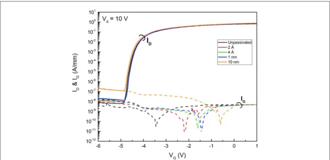
Table1lists the DC measurement results and calculated gate lag percentages for different devices, that are, unpassivated, 2 Å, 4 Å, 1 nm, and 10 nm ALD deposited Al2O3. Figure3compares the transfer characteristics
and gate currents of the devices for each passivation scheme, at VD=10 V. The threshold voltage was obtained
as−4.06 V for the unpassivated device using linear extrapolation at maximum linear slope and does not vary significantly for 2 Å, 4 Å, and 1 nm Al2O3passivation. For 10 nm ALD Al2O3passivation, Vthdecreases to
−4.15 V, analogous to the decrease observed in the C-V measurement, due to the increased sheet charge from the passivation layer. The measured output characteristics are shown in Figure4. The drain current density Idss
(at a gate voltage of VG=1 V) was obtained as 0.75 A mm−1for the unpassivated reference device, which
increased slightly by 5% to a value of 0.79 A mm−1for the 4 Å and 1 nm passivation scheme and by 10% to a maximum value of 0.82 A mm−1for the 10 nm passivation scheme. Similarly, the peak transconductance value increased by 4.7% from 179 mS mm−1for the reference device to 188 mS mm−1for the devices with 1 nm and 10 nm passivation. An improvement in knee voltage is observed with increasing Al2O3passivation thickness.
The reason for these improvements in the drain current characteristics is related to enhanced electron transport caused by an increase in sheet carrier concentration, due to the reduction in surface states.
The drain leakage current Id,leakis extracted from the transfer characteristics measurements as the current at
VG=−6 V and VD=10 V. Id,leakincreases monotonically with passivation layer thickness, which is also
Figure 2. Calculated values of trap conductance as a function of angular frequency for unpassivated, 2 Å, 4 Å, and 10 nm ALD Al2O3
passivated AlGaN/GaN HEMTs.
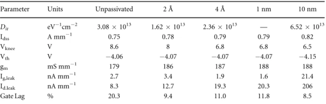
Table 1. List of measurements for devices with no passivation, 2 Å, 4 Å, 1 nm, and 10 nm ALD grown Al2O3.
Parameter Units Unpassivated 2 Å 4 Å 1 nm 10 nm
Dit eV−1cm−2 3.08×10¹³ 1.62×10¹³ 2.36×10¹³ — 6.52×10¹³ Idss A mm−1 0.75 0.78 0.79 0.79 0.82 Vknee V 8.6 8 6.8 6.8 6.5 Vth V −4.06 −4.07 −4.07 −4.07 −4.15 gm mS mm−1 179 186 187 188 188 Ig,leak nA mm−1 2.7 3.4 1.9 1.6 21.4 Id.leak nA mm−1 8.3 12.7 19.3 20.3 206 Gate Lag % 20.3 9.4 11.0 11.8 8.5
attributed to the increasing sheet charge of the 2DEG. The Schottky characteristics of the AlGaN/GaN HEMTs were measured with afloating drain contact (Figure5) and the gate leakage current Ig,leakis obtained from this
measurement as the gate current at VG=−6 V. The reverse gate leakage current, in contrast to the drain leakage
current, does not follow a monotonically increasing trend, indicating that the reverse gate leakage current is not dominated by surface leakage. The reverse gate leakage current increases for the initial passivation 2 Å, decreases for the two subsequent passivation thicknesses, then increases to its highest value for the greatest passivation thickness of 10 nm. The dominant mechanism of gate leakage is attributed to be edge gate leakage current, as the trend of the reverse gate leakage current for increasing passivation thickness correlates inversely with the trend in the gate lag characteristic. A decrease in gate lag corresponds to an increase in gate leakage, indicating that extension of the gate depletion region towards the drain by the virtual gate effect acting to disperse the electric field lines induced by the depletion region reduces the edge current [22]. Passivation that suppresses the virtual
gate thereby leads to an increase in gate leakage current. Low forward gate leakage current and nearly constant gate turn on voltage is maintained for each passivation scheme.
To further understand the correlation between the passivation layer and the surface states gate lag measurements were carried out. The gate lag measurements were performed using an Agilent E3631A power supply, Keysight Technologies 33500B waveform generator, and a Keysight InfiniVision DSOX2004A
Figure 3. Transfer characteristics and gate leakage for unpassivated, 2 Å, 4 Å, 1 nm, and 10 nm ALD Al2O3passivated AlGaN/GaN
HEMTs.
Figure 4. Output characteristics for unpassivated, 2 Å, 4 Å, 1 nm, and 10 nm ALD Al2O3passivated AlGaN/GaN HEMTs.
oscilloscope. The measurements were carried out by pulsing the gate from−6 V to 0 V, with a pulse width of 1 μs and period of 20μs with the drain kept at 0 V. The pulsed drain current response with respect to the DC values are compared in Figure6for the studied passivation schemes. A gate lag of 20.9% is obtained for the
unpassivated device, which improves by 55% to a gate lag value of 9.5% for the device with 2 Å passivation. For the 4 Å and 1 nm Al2O3passivation layers, a slight increase in the gate lag characteristics is observed, however,
significant improvement compared to the unpassivated case is maintained. For 10 nm Al2O3passivation layer
the lowest gate lag of 8.7% is observed.[23] reports that for ALD Al2O3passivation thicknesses between 10 nm
and 40 nm, increasing passivation thickness leads to decreasing current collapse, enabling the reduction of the current collapse below 15%. The results of this study indicate the same trend if passivation layers greater than 10 nm were studied, however, it is demonstrated that similar reduction in current collapse can be achieved with passivation layers as thin as 2 Å.
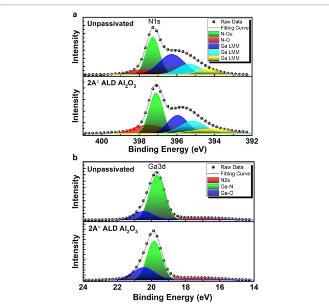
To gain insight on the passivation property of ALD Al2O3layer, x-ray photoelectron spectroscopy(XPS) is
utilized for unpassivated and 2 Å Al2O3coated samples. Before ALD process, all the samples have been treated
with a diluted HCl acid to remove the natural oxide layer. Figure7shows the N1s and Ga3d spectra of these two samples. Peak position correction was calibrated by referencing the C1s orbital peak position(284.8 eV) and the other peaks in the spectrum were shifted accordingly. As previously explained in several reports, the dominant surface defects of GaN are Ga and N vacancies(or dangling bonds). Based on the calculation of free energy by classical nucleation theory, most of the oxygen-derived hydroxyl groups such as OH radicals and H2O or O2will
Figure 5. IG-VGScharacteristics measured withfloating drain contact for unpassivated, 2 Å, 4 Å, 1 nm, and 10 nm ALD Al2O3
passivated AlGaN/GaN. HEMTs.
Figure 6. Drain current response of the pulsed gate voltage normalized to DC values with VD=0 V and VGpulsed from−6 V to 0 V
for unpassivated, 2 Å, 4 Å, 1 nm, and 10 nm ALD Al2O3passivated AlGaN/GaN HEMTs. The pulsewidth is 1 μs at 5% duty cycle.
be chemisorbed near imperfections such as dangling bonds and vacancies. Looking back into Figure7(a), the
N1s spectra is deconvoluted intofive main peaks [24]; three of which are assigned into Auger Ga LMM peaks, the
dominant one comes from the Ga-N bond, and the one in the higher energy tail is attributed to N-O bonds. As we can see, the passivated sample has a stronger N-O related peak. During the ALD process, the Ga vacancy positions are passivated by oxygen molecules and form these N-O bonds. On the other side, the Ga3d spectra can be scrutinized to gain a further insight on the surface properties of the GaN layer. As illustrated in Figure7(b),
this spectrum is deconvoluted into three Gaussian profiles [25]; a broad and weak response originated from N2s
orbitals, a dominant peak assigned to Ga-N bond, and a high energy response from Ga-O bonds. Looking at these peaks, it can be clearly seen that the Ga-O related peak is more dominant for 2 Å Al2O3passivated case
(compared to the unpassivated one). Therefore, similar to N1s data, the Al2O3passivation layer will substitute N
vacant positions and facilitate formation of Ga-O bonds. All the above-mentioned results confirm the efficient passivation of surface traps upon coating with the 2 Å Al2O3layer. Oxygen-containing gas molecules tend to be
chemisorbed on the surface of a semiconductor host through the capture of free electrons. Consequently, these chemisorbed radicals reduce the density of free carriers in the vicinity of the semiconductor surface and deplete the surface electron states. This, in turn, triggers the existence of the space charge region and induces band bending near the interface. On the other hand, these chemisorbed oxygen molecules are likely attached into trap states and dangling bonds. The passivation of surface traps, infirst ALD cycles, reduces the surface traps density, mitigates adsorption of oxygen radicals, and consequently reduces band bending. However, as we go to larger ALD cycles, bulk trap states in Al2O3layer start to become dominant and therefore diminish the
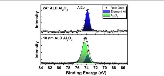
abovementioned characteristics. Moreover, the Al2p spectra have been extracted for 2 Å and 10 nm coated samples. As Figure8clearly illustrates, the portion related to Al element is the major peak for the thin passivated sample. However, as we increase the Al2O3layer thickness to 10 nm, the spectrum is mainly attributed to the
Figure 7.(a) N1s and (b) Ga3d high resolution XPS pattern of the resulting unpassivated and 2 Å thick Al2O3coated samples,
respectively.
oxide related peak. Thus, thefirst two ALD cycle just passivates the defect states and does not form a continuous Al2O3layer. However, the subsequent cycles trigger the formation of a continuous layer.
4. Conclusion
In conclusion, an angstrom-thick ALD Al2O3dielectric is reported for the passivation of surface traps in AlGaN/
GaN HEMTs and passivation thicknesses up to 10 nm are studied. For the a passivation layer as thin as 2 Å Al2O3, a greater than 50% improvement in gate lag compared to the unpassivated device is achieved.
Improvements in DC characteristics such as drain current density, knee voltage, and transconductance are observed. XPS analysis confirms that Ga vacancy positions are are passivated by oxygen molecules for Al2O3as
thin as 2 Å.
Acknowledgments
This work is supported by the TUBITAK under Project No. 116F041. One of the authors(E.O.) also acknowledges partial support from the Turkish Academy of Sciences.
ORCID iDs
Melisa Ekin Gulseren https://orcid.org/0000-0002-9375-2337 Gokhan Kurt https://orcid.org/0000-0002-1210-4013
Bayram Butun https://orcid.org/0000-0003-0892-4681
References
[1] Mishra U K, Parikh P and Wu Y-F AlGaN/GaN HEMTs-an overview of device operation and applications Proc. IEEE90 1022–31
[2] Chen K J et al GaN-on-Si power technology: devices and applications IEEE Trans. Electron Devices64 779–95
[3] Chung J W, Hoke W E, Chumbes E M and Palacios T AlGaN/GaN HEMT with 300-GHz fmaxIEEE Electron Device Lett.31 195–7
[4] Lu W, Kumar V, Schwindt R, Piner E and Adesida I 2002 A comparative study of surface passivation on AlGaN/GaN HEMTs Solid-State Electronics46 1441–4
[5] Vertiatchikh A V and Eastman L F 2003 Effect of the surface and barrier defects on the AlGaN/GaN HEMT low-frequency noise performance IEEE Electron Device Lett.24 535–7
[6] Edwards A P, Mittereder J A, Binari S C, Katzer D S, Storm D F and Roussos J A 2005 Improved reliability of AlGaN-GaN HEMTs using an NH3plasma treatment prior to SiN passivation IEEE Electron Device Lett.26 225–7
[7] Lee J-S, Vescan A, Wieszt A, Dietrich R, Leier H and Kwon Y-S Small signal and power measurements of AlGaN/GaN HEMT with SiN passivation Electron. Lett37 130–2
[8] Green B M, Chu K K, Chumbes E M, Smart J A, Shealy J R and Eastman L F The effect of surface passivation on the microwave characteristics of undoped AlGaN/GaN HEMTs IEEE Electron Device Lett.21 268–70
[9] Yatabe Z, Asubar J T and Hashizume T 2016 Insulated gate and surface passivation structures for GaN-based power transistors J. Phys. D: Appl. Phys.49 393001
Figure 8. Al2p high resolution XPS pattern of the resulting 2 Å thick and 10 nm Al2O3coated samples.
[10] Liu C, Chor E F and Tan L S 2007 Enhanced device performance of AlGaN/GaN HEMTs using HfO2high-k dielectric for surface
passivation and gate oxide Semicond. Sci. Technol.22 522
[11] Kordoš P, Kúdela P, Gregušová D and Donoval D 2006 The effect of passivation on the performance of AlGaN/GaN heterostructure field-effect transistors Semicond. Sci. Technol.21 1592
[12] Koehler A D et al Atomic layer epitaxy AlN for enhanced AlGaN/GaN HEMT passivation IEEE Electron Device Lett.34 1115–7
[13] Kim D et al 2007 ALD Al2O3passivated MBE-grown AIGaN/GaN HEMTs on 6H-SiC Electron. Lett43 129–30
[14] Wang H, Chung J W, Gao X, Guo S and Palacios T 2010 Al2O3passivated InAlN/GaN HEMTs on SiC substrate with record current
density and transconductance Phys. Status Solidi C7 2440–4
[15] Chung J W, Saadat O I, Tirado J M, Gao X, Guo S and Palacios T 2009 Gate-recessed InAlN/GaN HEMTs on SiC substrate Al2O3
Passivation IEEE Electron Device Lett.30 904–6
[16] Hashizume T, Nishiguchi K, Kaneki S, Kuzmik J and Yatabe Z 2018 State of the art on gate insulation and surface passivation for GaN-based power HEMTs Mater. Sci. Semicond. Process.78 85–95
[17] Ghobadi A, Ghobadi T G U, Karadas F and Ozbay E 2018 Angstrom thick ZnO passivation layer to improve the photoelectrochemical water splitting performance of a TiO2nanowire photoanode: the role of deposition temperature Sci. Rep.8 16322
[18] Li T C et al Surface passivation of nanoporous TiO2via atomic layer deposition of ZrO2for solid-state dye-sensitized solar cell
applications J. Phys. Chem. C113 18385–90
[19] Pascoe A R, Bourgeois L, Duffy N W, Xiang W and Cheng Y-B 2013 Surface state recombination and passivation in nanocrystalline TiO2dye-sensitized solar cells J. Phys. Chem. C117 25118–26
[20] Chandiran A K et al 2012 Subnanometer Ga2O3tunnelling layer by atomic layer deposition to achieve 1.1 V open-circuit potential in
dye-sensitized solar cells Nano Lett.12 3941–7
[21] Schroder D K 2006 Semiconductor Material and Device Characterization. (Hoboken, NJ, USA: Wiley)
[22] Chen Y, Ma X, Chen W, Hou B, Zhang J and Hao Y 2015 Influence of the gate edge on the reverse leakage current of AlGaN/GaN HEMTs AIP Adv.5 097154
[23] Lee D S et al 2012 Impact of Al2O3Passivation Thickness in Highly Scaled GaN HEMTs IEEE Electron Device Lett.33 976–8
[24] Stoklas R et al 2017 Influence of oxygen-plasma treatment on AlGaN/GaN metal-oxide-semiconductor heterostructure field-effect transistors with HfO2by atomic layer deposition: leakage current and density of states reduction Semicond. Sci. Technol.32 045018
[25] Huang R et al 2018 Angular dependent XPS study of surface band bending on Ga-polar n-GaN Appl. Surf. Sci.440 637–42