OF BII.KEN I UNIVERSn V
IN PARTIAL FULFILLMENT OF THE REQljlEKMEiNTS FOR THE DEGREE OF
MASTER OF SCIENCE Q C £ > S t
J<5B
l o o o hyit iv iy a tSILICON-ON-INSULATOR OPTICAL
WAVEGUIDES AND WAVEGUIDE DEVICES
A THESIS
SUBMITTED TO THE DEPARTMENT OF PHYSICS AND THE INSTITUTE OF ENGINEERING AND SCIENCE
OF BILKENT UNIVERSITY
IN PARTIAL FULFILLMENT OF THE REQUIREMENTS FOR THE DEGREE OF
MASTER OF SCIENCE
By
Isa Kiyat
September 2000
Äooo
I certify that I have read this thesis and that in my opinion it is fully adequate, in scope and in quality, ^is a dissertation for the degree of Master of Science.
Prof. Atilla Aydinlil (Supervisor) I certify that I have read this thesis and that in my opinion it is fully adequate, in scope and in quality, as a dissertation for the degree of Master of Science.
Assoc. Prof. Recai Elfialtioglu I certify th at I have read this thesis and that in my opinion it is fully adequate, in scope and in quality, as a dissertation for the degree of Master of Science.
Asst. Prpfi Serdar Özgelik
Approved for the Institute of Engineering and Science:
Prof. Mehm^ Baray,
SILICON-ON-INSULATOR OPTICAL WAVEGUIDES
AND WAVEGUIDE DEVICES
♦
Isa Kiyat
M. S. in Physics
Supervisor: Prof. Atilla Aydınlı
September 2000
Silicon-on-insulator(SOI) optical waveguides, directional couplers and some types of MMI couplers were designed, fabricated and characterized at a wavelength of 1.55 /im. Effective index method and the single mode condition for rib waveguide was used in design of optical waveguides. BPM simulations were extensively employed for all fabricated devices. Waveguides and the other devices were defined on SOI material by wet chemical etching in KOH solutions^ Fabricated devices were characterized on a standard fiber optic measurement setup with a DFB laser as its IR light source. In characterization of optical waveguides the single mode condition was verified and insertion loss was measured to be 12.2 dB for TE and 12.7 dB for TM polarized light as the best values. Furthermore, the propagation loss found to be 0.70 dB /cm for TE and 0.76 dB/cm for TM which is typical . Characterized directional couplers gave results completely consistent with their BPM simulations. 1x2, 2x2, 1x4 and 1x8 type MMI couplers were also found to gave expected behaviors. Splitting ratios as low as 0 dB and 0.55 dB was measured.
K eyw ords: Integrated optics, silicon-on-insulator(SOI), optical waveguide, single mode condition, BPM, optical loss, butt coupling, anisotropic KOH etching, directional coupler, multimode interference(MMI), MMI coupler.
YALITKAN USTU SİLİSYUMA DAYALI OPTİK
DALGA KILAVUZLARI VE DALGA KILAVUZUNA
DAYALI AYGITLAR
İsa Kiyat
Fizik Yüksek Lisans
Tez Yöneticisi: Prof. Atilla Aydınlı
Eylül 2000
Yalıtkan üstü silisyuma dayalı dalga kılavuzları, doğrusal çiftleyiciler ve bazı çeşit çok kipli girişim çiftleyicilerinin tasarımı, üretimi ve 1.55 yum dalga boyunda karakterizasyonu yapıldı. Optik dalga kılavuzlarının tasarımında etkin indis yöntemi ve sırt dalga kılavuzları için tekil kip koşulu bağıntısı kullanıldı. Ayrıca, BPM simlasyonları yoğun olarak kullanıldı. Dalga kılavuzları ve diğer aygıtlar KOH çözeltisi içinde izotropik olmayan ıslak aşındırma yöntemiyle oluşturuldu. Üretilen cihazlar, DFB kızıl ötesi lazer kaynağı olan standart bir fiber optik ölçüm düzeneğinde karakterize edildi. Optik dalga kılavuzu karakterizasyonunda tekil kip şartı teyit edildi ve optik giriş kaybı TE polarize ışık için en iyi değerler 12.2 dB ve TM polarize ışık için 12.7 dB olarak ölçüldü. Ayrıca optik iletim kaybı da TE için 0.70 dB/cm ve TM için 0.76 dB /cm olarak bulundu. Karakterize edilen doğrusal çiftleyiciler BPM simülasyonlarıyla tamamen tutarlı sonuçlar verdi. Ayrıca, 1x2 ve 2x2 çok kipli girişim çiftleyicilerin de beklenen özellikler gösterdiği tespit edildi. 0 dB ve 0.55 dB kadar küçük ayrılma oranları ölçüldü.
Anahtar
sözcükler: Tümleşik optik, yalıtkan üstü silisyum, optik dalga kılavuzu, tekil kip şartı, BPM, optik kayıp, uçuca çiftleme, izotropik olmayan KOH aşındırması, doğrusal çiftleyici, çok kipli girişim, çok kipli girişim çiftleyicisi.
I would like to express my deepest gratitude to Prof. Dr. Atilla Aydınlı for his supervision during research, encouragement and friendly understanding throughout this thesis work. I would like thank Alpan Bek for all his help during the early stage of this work.
I would like also thank Murat Cure, Gungur Sincer and all the other ARL people for their help in making ARL a good research environment.
My many thanks are to Özgür Çakır, Emre Tepedelenlioğlu, Feridun Ay, M. Ali Can, Selim Tanrıseven, Kerim Savran, Kamil Erkan, Sefa Dağ, İbrahim Kimukin and Mehmet Bayındır for being what a friend should be and their moral support.
I would like to dedicate this thesis to my family who have given continuous support throughout my life and Evla for her love and support throughout this work.
Contents
Abstract i
Özet iii
Acknowledgement v
Contents vi
List of Figures viii
List of Tables xi
1 Introduction 1
1.1 Integrated O p t i c s ... 2
1.2 Silicon and Silicon-on-insulator (SOI) in Integrated Optics . . . . 4
2 Theoretical Considerations 9 2.1 Analysis of Optical W aveguide... 10
2.2 Single Mode Waveguide and Single Mode C o n d itio n ... 17
2.3 Loss in Optical Waveguides ... 22
2.3.1 Optical Waveguide Loss M e ch a n ism s... 23
2.3.2 Measurement of Optical Waveguide L o s s e s ... 24
2.4 Optical Waveguide Directional Couplers ... 27
2.5 Optical Multi-Mode Interference(MMI) C ouplers... 32
2.5.1 Important Issues in Design and C haracterization... 36
3.2 Sample P re p ara tio n ... 43
3.2.1 Sample C le a n in g ... 43
3.2.2 Masking Material Deposition 44 3.3 Photolithography; Pattern T r a n s f e r ... 46
3.4 Anisotropic KOH etch in g... 48
4 Measurements and Characterization 58 4.1 Thickness Measurement Results of SOI Wafers U se d ... 58
4.2 Characterization of SOI Optical Single Mode W aveguides... 62
4.2.1 Measurement S e tu p ... 62
4.2.2 Verification of Single Mode C o n d itio n ... 64
4.2.3 Optical Waveguide Loss Measurement 68 4.3 Characterization of Optical Directional C o u p lers... 73
4.4 Characterization of Optical MMI C o u p le rs ... 78
4.4.1 The Mask D e s ig n ... 79
4.4.2 Measurements and R e s u lts ... 80
4.4.3 D isc u ss io n s... 88
5 Conclusions and Discussions 90
List o f Figures
2.1 Slab Waveguide S t r u c t u r e ... 10
2.2 The Light rays in a slab waveguide; for confined (a) and not confined (b) light... 12
2.3 TE and TM polarizations in slab w a v e g u id e ... 12
2.4 A schematic of light in the slab waveguide as waves and rays. . . . 15
2.5 TE modes in a SOI slab waveguide with thickness of 1 //m. 16 2.6 Types of rectangular dielectric w a v eg u id e s... 18
2.7 EIM analysis of a rib w aveguide... 19
2.8 Single Mode Condition for rib waveguides with H=3,4and 5 /xm. . 22
2.9 Schematic layout of a directional c o u p le r ... 28
2.10 Cross section of a rib waveguide directional coupler (a) and its EIM counterpart (b) 29 2.11 The power exchange between waveguide A and B ... 31
2.12 Some MMI coupler exam ples...· · · 32
2.13 Lateral modes in a multimode waveguide with metal(a) and semiconductor(b) w a lls ... 33
3.1 A picture of SOI s tr u c tu r e ... 40
3.2 Process layout of BESOI and sm art — cut te c h n o lo g ie s... 42
3.3 PECVD reactor structure ... 45
3.4 Effect of the waveguide strip orientation on the waveguide profiles on (100) su rfa ce ... 49
3.5 SEM photograph of the initial etching results; waveguide profile . 50 3.6 SEM photograph of the initial etching results; s u rfa c e ... 50
3.8 The etching results at 35 °C; surface and waveguide walls... 52 3.9 The etching results at 30 °C; surface and waveguide walls... 52 3.10 SEM photograph of a cross section of a SOI waveguide fabricated
by KOH etching... 53 3.11 A top view photograph of SOI directional couplers fabricated by
KOH etching; the lines closer to each other are straight waveguide
sections... 53 3.12 Top view photographs of input and output ports of SOI MMI
couplers fabricated by KOH etching... 54 3.13 SEM photograph of a bad (not optically cleaved) waveguide facet. 55 3.14 Photograph of optically cleaved waveguide facets... 56 3.15 All steps in fabrication of SOI optical waveguides... 57 4.1 A slice taken from a wafer for layer thickness measurement... 59 4.2 SEM photographs of layers taken at (a) 0.8 mm and (b) 39 mm to
the wafer edge for Wafer 2... 60 4.3 Measured layer thicknesses for Wafer 1... 60 4.4 Measured layer thicknesses for Wafer 2... 61 4.5 BPM simulations of optical power confinement for a SOI rib
waveguide of different Si02 layer thicknesses... 61 4.6 DFB laser wavelength peak value variation with laser temperature. 62 4.7 Optical measurement setup... 64 4.8 Transverse fundamental and first excited mode profiles of a SOI
SM (a) and MM (b) waveguide structure computed using BPM. . 65 4.9 Comparison of BPM simulation results (b) with SM condition
results (a)... 66 4.10 ТЕ and TM fundamental modes of a single mode waveguide on
sample SMSOI09... 68 4.11 Output images of an output port of SOI waveguides on sample
SOIMMI05 with different alignments... 69
4.12 Slopped rib facets after a standard optical quality cleavage... 70 4.13 Measured insertion losses versus waveguide length... 72 4.14 Output images and peak profiles at different straight section
lengths(L)... 75 4.15 Coupling ratios and fitting curves for the characterized couplers. . 76 4.16 BPM simulation results of straight sections only: X Z counterparts
and coupling ratios for both TE and TM, L=4250 //m... 77 4.17 BPM simulation results, s-bends included: X Z counterpart and
coupling ratios for TE and L=1250 ¡xm... 78 4.18 BPM simulation results for 1x2 MMI power splitters and 2x2 MMI
couplers... 81 4.19 BPM simulation results for 1x4 and 1x8 MMI power splitters. . . 82 4.20 Output port images of 1x2 MMI power splitters for various MMI
section len g th s... 84 4.21 Measured splitting ratio versus MMI section length for 1x2 devices
of 48 yum width... 85 4.22 Output port images of 2x2 MMI couplers for various MMI section
lengths... 86 4.23 Measured splitting ratio versus MMI section length for 2x 2 MMI
couplers of 36 ¡jm width... 87 4.24 Measured splitting ratio versus MMI section length for 2x 2 MMI
couplers of 64 /¿m width... 87 4.25 Output port images of 1x8 and 1x4 MMI power splitters for various
1.1 Optically active and passive materials for O I C ... 3 3.1 The recipe file parameters used for deposition of Si3N4, masking
film... 46 4.1 The thicknesses of SOI wafers used... 58 4.2 The geometrical dimensions of analyzed SOI optical waveguides. . 67 4.3 Typical measured insertion losses... 71 4.4 Geometrical dimensions of the characterized directional couplers . 73 4.5 List of MMI structures on the designed mask... 80
Chapter 1
Introduction
’’Knowledge is Power”, has said one ad campaign, a simple, clear and self explained statement. Instead, if we are asked ”Is Knowledge Power?”, most of us would say ”Of course!”.
Information and its distilled form, knowledge, is gaining more importance in our lives day by day. It is nearly impossible to imagine that we live without computers, televisions, satellites, undersea fiber networks, cellula.r phones, fax machines, printers, and all other devices used to produce, transfer, manipulate and access information.
The electronic devices, mainly the mass produced high density semiconductor devices have played the important role in the modern information age. The information processing speed is the most remarkable feature of these devices. Are the electronic devices the only solution for the information age? To answer this question, the demands of the information age on candidate devices and technologies must be well understood, which are met by the electronic devices to some extent. These demands may be stated as the following,^ information reception (detection), information enhancement (amplification), in formation manipulation, memory, information transfer, information generation, and information display. We know from the advances in the last few decades that there is an alternative technology named integrated optics -exploiting light- and/or integrated optoelectronics -exploiting both light and electrons.
1.1 Integrated Optics
Instead of cables, the metal interconnects and integrated electronic circuits in the integrated electronics, light guiding optical fiber, dielectric waveguides and optical integrated circuits (OIC) are utilized in integrated optics, respectively. Integrated optics showed great progress in meeting the demands of information age since 1960’s, with the development of the laser as a stable source of coherent light.^ References(^) and (^)are very good sources for a historical overview of integrated optics.
There are some points where integrated optic devices (optical fibers and QIC’s) have advantages over electronic devices. Electronic devices have limitations on the inter-connectivity due to metal interconnects, difficulties in transmission of information over long distances -integrated optics has showed the most significant development in this area by using optical fiber networks- , external electromagnetic interference effects, small bandwidth, comparatively large size and heavy weight and scattering of electrons as they move in a material. Being totally different from the above criteria, no phase information could be kept in a system of electronic devices after some amount of distance. This does not bring any functional problem for the electronics devises, actually. However, this is a point where integrated optics will find new horizons. T hat is, capability of keeping phase information of light leads the emergence of new so-called ” future” devices in integrated optics which are based on ’’interference effect” .
Two forms of optical integrated circuits are widely used, hybrid QIC’s in which two or more substrate materials are bonded together and monolithic QIC’s in which a single substrate material is used for all components of the circuit. Since nearly all QIC’s need a light source, i.e. a laser, monolithic QIC’s can only be fabricated in optically active materials, that is, materials with direct bandgaps and capable of light generation. The materials that are incapable of light generation are optically passive. Both optically passive and active materials commonly used in fabrication of integrated circuits are presented in Table. 1.1.
CHAPTER 1. INTRODUCTION PASSIVE ACTIVE Quartz Lithium niobate Lithium tantalate Tantalum pentoxide Niobium pentoxide Silicon Polvmers Gallium arsenide Gallium aluminium arsenide
Gallium arsenide phosphide Gallium indium arsenide
Other III-V semiconductors with direct bandgaps Other II-VI semiconductors with direct bandgaps
Table 1.1: Optically active and passive materials for OIC
aluminum arsenide, G ai-xAC As or the gallium indium arsenide phosphide
G axIni-xAsi-yP y. One of the most important properties of these optically
active materials is that by changing the fractional atomic concentration of the constituents, the emitted wavelengths can be varied from 0.65 ^m (for AlAs) to 1.7
¡j,7n (for GalnAs). The other important properties which deserve to be mentioned
are the following: firstly, these materials are transparent for wavelength range of 0.6 fxm to 12 y.m and have relatively large electro optic and acoustooptic properties. Then, the nearly equal lattice constants of GaAs and AlAs (5.646 and 5.369 A, respectively)® makes epitaxial growth of layers of G ai-xA lxA s with greatly different A1 concentration possible with minimal interfacial strain being introduced. Finally, they are the cheapest of all III-V and II-VI materials, due to their widespread use. These materials are used in fabrication of all type OIC’s components, but especially preferred for the fabrication of multilayered heterojunction lasers.
Lithium niobate, LiNhOz is an anisotropic material with high electrooptic and acousto-optical coefficients. It is transparent for the range of 0.2 fim to 12
fim. LiNbOz based hybrid OIC’s are the most commercialized integrated optic
systems. Nearly all of the integrated optic devices first realized on LiNbOz except lasers and detectors. Apart from these properties it has a very high birefiringence which makes it a good material for polarization sensitive d e v i s e s . A n o t h e r optically passive materials group is polymers which represents a huge class of
materials. Among them, poycarbonate which used for compact discs and PMMA (photoresist) are used for purely passive optical components.® Other poymers exhibit a large elctro-optical or nonlinear coefficient, but at the expense of a poor long term stability. Silicon, which is also optically passive, based technologies are mentioned in the next section.
Optical waveguides are one of the building blocks of integrated optic technology. Waveguides have been realized in different types and geometries planar, circular, rib, ridge, buried etc. In both optically passive and active materials including those briefly explained here. The loss characterization is the key step when analyzing a waveguide. The losses of as large as 2-5 d B fc m for GaAlAs systems, 0.5 d B /cm for LiNhOz, and 0.1 d B /c m for silicon based optical waveguides are typical.^ Apart from being fabricated and analyzed as a separate devices, optical waveguides are passive components of most of the integrated optical devices, e.g. in directional couplers, multimode interference couplers, modulaters, Mach-Zehnder type devices, access components of detectors and lasers in QIC's, etc.
1.2 Silicon and Silicon-on-insulator (SOI) in
Integrated Optics
Integrated optics on silicon has received great attention especially in the last decade. A very clear reason may come to mind immediately. T hat is, since silicon is the most commonly used material in semiconductor electronics,it is commercially available in high quality and at low prices. Hence, it is natural to investigate silicon as a candidate platform for integrated optics. But, why to have waited until late 1980’s. The answer hide in the latest developments in silicon materials technology® (other than bulk silicon), first with the emergence of silicon-on-insulator(SOI) as a platform for both QIC’s and electronic integrated circuits (e.g. VLSI,CMQS, etc.), second epitaxial growth of silicon based alloys with tailored optical properties ( SiCe-heterostructures) and doped silicon. There
CHAPTER 1. INTRODUCTION
are some other technologies such as silica on silicon and siliconoxynitride(SiON) films. However, they use silicon only as substrate material.
Plasma enhanced chemical vapor deposition (PECVD) or f ame hydroli- si.s(FHD) techniques are used to deposit silica layers on silicon or quartz substrates. Then the substrates are heated to about 1000 C° to make glass layers transparent. These silica layers are designed such that refractive index differences of 0.5-1.5 percent are possible. This flexibility is useful for different applications. That is low refractive index difference is good for low loss devices whereas, high refractive index difference allows fabrication of bend-waveguides with smaller radii. The typical waveguide losses in this technologv- ranges from 0.01 d B /cm for low refractive index difference and large core sizes to 0.07
d B ic m for high refractive index and small core sizes.® On the other hand,
in SiON technology, SiOX layers with refractive indices between 1.45 (silicon- oxide refractive index) and 2 (silicon-nitride refractive index) are deposited by optimized PECVD or LPCVD techniques on an already deposited therm al silicon- oxide layer on a silicon substrate. Light guides in the SiON layer which has a slightly larger refractive index than lower cladding (thermal o.xide) and upper cladding (silicon-oxide deposited after waveguide fabrication). Before waveguide or device fabrication the deposited SiON layers are annealed at an approximate temperature of 1140 °C. This step is needed to remove N-H bonds which exist in deposited SiON layers. These bonds cause an infrared absorption and its first overtone is found at 1510 nm which is very near to the optical communication wavelengths, 1550 nm. The typical losses for SiON based waveguide technology are 0.1 dB/cm for slab waveguides and 0.2 dB/cm for channel waveguides. One of the most important advantages of the SiON technology with respect to weakly guiding materials technologies is that waveguide bend radius as small as 1.5 mm are possible due to the high refractive index difference between SiON layer and its cladding.^®
In doped epitaxial silicon based waveguides, guiding is obtained if the doping level of the epilayer is lower than the doping level of the substrate. However, these waveguides suffer from high optical losses, waveguide loses in the range of
15-20 d B /cm have been measured for rib waveguides with epilayers of thickness between < H < AZum and doping levels of a few for epilayer and 10^® — 10^® cm"® for s u b s t r a t e . T h e s e high losses may be further decreased by using larger H and a very highly doped substrate, because the main source of the loss is the substrate absorption. Applying the above statement the optical losses as low as 1.2-1.5 dB/cm have been achieved.
Si-Ge heterostructures can be fabricated by both MBE^® or CVD-growth.^^’®® Germanium(n ~ 4.3) is used to slightly increase the refractive index of silicon (n ~ 3.5). For a resultant ¿'¿i-^Gei-alloy, nsioe ~ + 0.3x -f 0.32a;^ gives refractive index which is enough for weakly guiding structures. Due to the similar lattice constants of Si and Ge which both are belong to group IV of the periodic table, epitaxial growth of thin strained SiGe-layers is possible. Waveguides on MBE-grown strained 5 io.99Gco.oi layer have been fabricated with losses 3- 5 d B /cm at A = 1.3/im^® and with reduced loss of 0.6 d B /c m on CVD-grown
Sii-xC cx layers.*® The high cost and difficulty in growing of SiGe by MBE and
CVD, lead induffusing of germanium into commercially available silicon. SiGe is a good platform for photodetector fabrication and these devices have been integrated with SOI waveguides.*^ So SiGe is an important material due to its compatibility with SOI technology. Most of the integrated optical components and devices have been realized on the materials mentioned here, we do not attem pt to include all these information here which would be a lengthy task.
Among these silicon based materials, SOI -apart from its promises in future electronic integrated circuits- has very unique optical properties due to its very unique structure. It uses pure silicon as its guiding layer and has a large refractive index difference between silicon( n ~ 3.5 and Si02{n ~ 1.45). Silicon has very good optical properties at the optical telecommunication bandwidth (around 1.3^ m and 1.55pm) and it is fully compatible with silicon electronic integrated circuit. Since, full replacement of integrated electronics with integrated optics will probably not happen for a very long time, this compatibility is one of SOI QIC’s most important advantages over other technologies.
CHAPTER 1. INTRODUCTION
on the well-established silicon integrated electronics micromachining technology.
So there is nearly no need to establish a new device fabrication technologies. Like bulk silicon SOI is now commercially available both at high quality and at relatively low prices. Although, there are a number of fabrication techniques of SOI substrate, only two of them has good material properties and have succeeded in becoming commercial, namely Separation by IMplemented OXygen (SIMOX) technology and Bond-and-Etchback (BE-SOI) technology,^® more information on these SOI fabrication techniques are given in section 3.1.
In last decade optical properties of SOI waveguides have been investigated and a number of both passive and active(based on electroptic effect) optical integrated devices on SOI developed. The fabrication techniques are not presented here , they are explained in Chapter 3 extensively. Waveguides on SOI was first realized with relatively high propagation losses then by means of advanced fabrication techniques this value come to 1 dB/cm , and then to 0.5 d B /cm , and finally to 0.1 d B /cm using large cross-section SOI rib waveguides. Typically, the losses around 0.5 dB /cm are obtained provided that silicon top layer is larger than 4
¡xm and waveguides are designed to be single mode. Also the dependence of
propagation loss on the thickness of insulator {SiO<i) has been investigated. Apart from optical waveguides, a number of SOI guided wave optical devices and circuits (SOI-OIC’s) have also been demonstrated. Some examples are integrated 2>dB directional couplers with excess insertion loss (that is chip loss) of 1.9 dB/^^ 5x9 star couplers with loss of 1.3 dB/^^ asymmetric Mach-Zehnder type wavelength filters with -18 dB crosstalk^^ and waveguide interferometers based on electroptic eifect^®(low eloctrooptic response of the silicon enhanced by ion implantation), optical switches based on thermoptic effect^®’®® with 5 fxs rise time and 150 m W switching power®® and low-loss multimode couplers.®
The ultimate purpose of this effort of which this work is only the first part, is the development of a library of low-loss silicon-on-insulator (SOI) optoelectronic devices. To reach this goal, SOI waveguides(singe and multimode), directional couplers and MMI couplers have been designed, simulated, fabricated and characterized to some extend so far. This thesis work summarizes
the fundamental physical theories behind these optical integrated devices in Chapter2, describes the each fabrication step in Chapters and explains the measurements and presents results in Chapter4.
Chapter 2
Theoretical Considerations
As was stated earlier, the optical waveguide being the integrated optics counterpart of the metallic interconnects in integrated electronics, is the fundamental component of optical integrated circuits. So it is necessary to analyze the optical waveguide before we try to study optical integrated devices. In this chapter, the slab waveguide and single mode waveguide at the beginning and is discussed first, then optical directional couplers and multimode interference (MMI) couplers are treated.
Light propagates in an optical waveguide in the so-called optical modes according to wave optics. In its simplest meaning, like its counterparts in many other physical situations, modes are the different ’’ways” of propagation of optical energy in a waveguide. These modes, can be differentiated from each other by spatial distribution of optical energy in the waveguide, the propagation constant and the orientation of electric and magnetic fields (polarizationj of the each mode. An optical waveguide can support a definite number of modes at a specific wavelength, the waveguide is called a single mode waveguide if only one mode is supported, and a multimode waveguide if more than one mode is supported. The number of modes for an optical waveguide is determined by its refractive index distribution, that is the refractive index values of materials making up the waveguide, and the waveguide geometrical dimensions.
the only. Ray optics (geometric optics) which assumes that light travels in straight lines ,is also useful in analyzing the optical waveguide. Ray optics is used whenever it is applicable and it is an approximation of the wave optics in the limit of small wavelengths and/or large waveguide or device dimensions, especially when the waveguides are multimoded.
Since we mainly deal with single mode waveguides which are very small in dimensions, wave optics will be used in most of the following sections. A brief summary of ray optics will also be given since the planar (slab waveguide) optical waveguide, which is the first step in understanding of the waveguide theory, can also be analyzed by ray optics.
2.1 Analysis of Optical Waveguide
>Being the simplest of waveguides, it is logical to analyze the slab waveguide first. Slab waveguides are very good models for studying more general types of optical waveguides. Slab waveguides are dielectric slab films.
i i M ‘ - f - "
Figure 2.1: Slab Waveguide Structure
As is seen in Fig. 2.1 , in general, it has a minimum of three different layers. For guidance of light, n / (refractive index of guiding film) must be larger than ric(refractive index of cladding layer) and (refractive index of substrate layer).
CHAPTER 2. THEORETICAL CONSIDERATIONS 11
U f > Us > Tic. (2.1)
''-’.’hen ns=ric, the slab waveguide is said to be sym m etric and antisym m etric otherwise, Ug 7^ ng. So the symmetric waveguides are special cases of ainisymmetric ones.
Since, the slab waveguide is an optical waveguide, all the rules apply to it. The slab waveguide supports a definite number of optical modes, and at least one if it is symmetric. These modes can be found by applying the boundary conditions to Maxwell’s equations. However,the same modes for slab waveguides can be found by using ray optics concepts which has a relatively easier procedure.
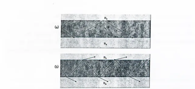
In ray optics, it is a.ssumed that a light ray in a homogeneous optical medium follows straight paths. Light .changes its path after passing from one medium to another with different refractive index, and the paths in different media have a relation between them through the well known Snell’s law. The Snell’s law relates the angles with respect to the normal to a dielectric interface that a beam forms when passing through the interface. For guiding of light, rays should be confined in the middle layer of the slab waveguide and this is only possible when total internal reflection (TIR) occurs. TIR happens when the angle of incidence is smaller than the so called critical angle of TIR. Light rays having angles of incidence smaller than this critical angle will be confined (see Fig.2.2). When the phase information of the light rays having multiple reflections on the interfaces is brought into picture, it is seen the only light rays which are incident at some specific angles are guided.
On the other hand, in wave optics, all analysis start with solving well known Maxwell equations for a source free (p=0, J = 0 ), linear (e and ¡j, are independent of E and H) and isotropic medium. Maxwell equations are strongly coupled. They can be decoupled through a standard procedure of creating a single second order differential equation. This procedure when applied to the Maxwell equations leads to
Figure 2.2: The Light rays in a slab waveguide; for confined (a) and not confined(b) light.
the wave equation and tp stands for either of E or H.
Now we can solve, the wave equation for the slab waveguide in Fig. 2.1. The parameters are chosen such that n / > n¡ > Uc and the guiding layer has thickness
h. To make the problem simpler, rectangular cartesian coordinate system can be
utilized. is always chosen to show propagation direction. There are two cases emerging from geometry, either E ov H is parallel to the layer interfaces, which define either TE or TM polarizations respectively as shown in Fig.2.3.
(TEPolarization) ^ " (TM Polarization)
■ ■ ·■ V . ' . · . · . i r v
CHAPTER 2. THEORETICAL CONSIDERATIONS 13
Also, TE and TM polarizations are preserved as the light propagates in z direction and undergoes reflections with respect to the rectangular cartesian coordinate system. The analysis will be done for TE, and can be similarly done for TM. In TE case, E only has Ey component and the electromagnetic radiation have the following general form.
Ê ( x ,y , z , t ) = È ( x ,y ) S “‘ (2.3) where P is the propagation constant in z direction. It is also called the longitudinal wavevector. u is the angular frequency given in terms of c, the speed of light and A. the wavelength of electromagnetic wave as.
u> = 27TC
T
(2.4)Then the wave equation, Eqn. 2.2 for Ey can be written as scalar wave eouation: here n(x) is given as and ko as
V^Ey + klri^{x)Ey =
0 (2.5) n{x) = Us X < - h Uf 0 > X > —h ric X > 0(
2.
6)
ko = 27T (2.7)E.j has no y dependence, since the slab waveguide is infinite in y direction. So, Erj can be written using Eqn. 2.3 as
Ey{x,z) = Ey{x)e-^^^
(
2
.
8
)
+ ( k y { x ) - a''-)E, = 0 (2.9) The solution to the Eqn. 2.9 changes according to sign of the value inside the parenthesis. The cases are,
and
E,(x) = i f p > k o n
Ey(x) = i f 0 < k „ n
(
2.
10)
(
2.
11)
where Eq is the field amplitude at x=0. The solution given in Eqn. 2.10 has a real exponential form and to be physically meaningful the solution with minus sign is chosen , which leads to a negatively decaying solution. The other case gives an oscillating solution. Two new coefficients are defined which are useful to understand the physical processes in the two cases. They are
Attaneuation Coefficient, 7 = \ J — k^'n? i f ^ > kon
Transverse Wavevector, k = ^kl'n? — ¡3- i f P < kon
(
2.
12)
The two cases are visually compared in Fig.2.4 according to both ray optic and wave optic approaches.
As seen clearly in the Fig. 2.1, for guidance or total internal reflection to take place, the condition of the Eqn. 2.1 can be restated as
koTis < P < koUf (2.13) Then the general solution of Ey for the slab waveguide can be written in either oscillatory or decaying waves according to Eqn. 2.13,
Ey = Ae~^^^ Ey = Bcos{Kfx) + Csin{Kfx) Ey = x > Q — < a; < 0 X < —h (2.14)
CHAPTER 2. THEORETICAL CONSIDERATIONS 15
Figure 2.4; A schematic of light in the slab waveguide as waves and rays. where the coeiRcients A, B, C and D will be determined from boundary conditions. There are two boundary conditions to be satisfied. Tangential E and H must be continuous at the interfaces. The first condition says Ey will be continuous. Utilizing Maxwell equations and the constitutive relations to find an e.xpression for the continuity of the tangential H results in
H, = — ^ ¡jujJ dx
y (2.16)
Applying these conditions will give us the coefficients in Eqn. 2.14, but instead we will find a more fundamental relation. After a few manipulations and applying the boundary conditions gives the so called the eigenvalue equation for /3 for TE polarization.
ta n {hKf) - 7c+ 75
«/(1 - (2.16)
The above equation is also called the characteristic equation of TE modes of a slab waveguide. Eqn. 2.16 is a transcendental equation and it can only be solved numerically or graphically.
Setting the problem for TM case and using the same procedure yields a relation, Eqn. 2.17, which is somewhat different;
tan (/*«/) — rU-f n·} , + TifTc] Kj (2.17) T'cTs
These complex looking equations are simplified for the special case of the symmetric waveguide. The eigenvalues of these eigenvalue equations, /3te and
Pt m can be found for a slab waveguide with a definite thickness h and index
values for its layers using either a numerical or graphical software in a personal computer. A simple example computation result using a graphical software is given in Fig.2.5.
Figure 2.5: TE modes in a SOI slab waveguide with thickness of 1 /tm. As seen in the example given in Fig.2.5 the waveguide confines a definite number of modes. This corresponds to existence of a definite number of eigenvalues of eigenvalue equation for /?, and a definite number of light rays traveling at different angles in the waveguide.
The number of modes, m, can be determined after plotting the eigenvalue equation, the number of nodes are equal to the number of modes supported, but there is a simple approximate formula as well:
CHAPTER 2. THEORETICAL CONSIDERATIONS 17
hk{nj
-m = I n t [— — ]
7T (2.18)
T :iis is an approximation only and in general good, when m is large. This equation g: ves im portant results. The number of modes that a waveguide confines increases as the difference between the refractive index of the guiding film and the substrate and the thickness of the film, h, increase. The numerator in the Eq. 2.18 is called the normalized frequency of the waveguide. This value is generally used to designate a waveguide. The number of modes is a key concept in design of waveguides and waveguide devices. If a signal with a narrow bandwidth is launched to a waveguide with m larger than one, the signal will be distributed o’- er all modes and since light moves with slightly different speeds in different modes, the signal will have Ihrger bandwidth after some distance. This effect will decrease the rate at which the signals can be sent. The single mode waveguide ccmes as an answer for this problem.
2.2 Single Mode Waveguide and Single Mode
Condition
The slab waveguide is easy to analyze and useful to understand the basic concepts of optical waveguides. However, it has no lateral confinement and this reduces the number of applications where it can be used. The alternatives are circular fibers and dielectric rectangular waveguides. The fibers are not compatible with planar processing technology, such as planar chips, which are backbones of integrated electronics. The slab waveguide can be laterally confined and resulting structure is I he so called dielectric rectangular waveguide. The rectangular waveguides may have several geometric shapes to establish the lateral confinement namely, rib waveguide (Fig.2.6a), ridge waveguide (Fig.2.6b), channel waveguide (Fig.2.6c) and diffused waveguide (Fig.2.6d). Rib and ridge waveguides have the same shape, th at is the top dielectric layer has a rib, the difference between them is th a t the guiding layer in ridge waveguide is the layer under the rib layer whereas
the rib layer functions as the guiding layer for rib waveguides.
c) Channel
¿."•"•b;/; 1
d) DifTused
Figure 2.6; Types of rectangular dielectric waveguides
The SOI optical wavegqide we designed, fabricated and characterized in this work is a very good example of the rib waveguide type. The mode analysis of the rectangular waveguides (i.e.: of the SOI waveguide) is a bit cumbersome and exact analytical solutions can not be so easily found, instead, some simplified analytical results based on the solution of the wave equation are further corrected by some perturbation techniques. W hat is actually needed are some simple methods which will be useful for design purposes. There are two waveguide design tools, namely effective index method (EIM), which is an relatively easy method to apply and useful for most of the design purposes and the beam propagation method (BPM), which is a numerical simulation method and not an approximation to the analytical solution. The SOI rib single mode waveguides were designed applying EIM, then BPM were also used for verification.
A rectangular waveguide can be analyzed in two dimensions (x and y) as seen in Fig.2.7. The effective index method comes into picture at this point, it divides the 2D problem into two ID problems (slab waveguides for which the exact solutions are straightforward).
In this method the rib waveguide is divided so that three slab structures are formed as seen in Fig.2.7. The propagation constant, j3, for the guiding mode of interest and wavelength are calculated from the eigenmode equations of the
CHAPTER 2. THEORETICAL CONSIDERATIONS 19
n,
effl n ef£2I ' ... .ij
^effl
Figure 2.7: EIM analysis of a rib waveguide
slab waveguide for the two slab waveguide structures. Then the effective indices
{n^ffi and neff2) are calculated for each structure using,
neff —I
ko (2.19)
Then, using these effective indices an artificial slab waveguide structure is formed as in Fig.2.7 and calculation of the ^ is repeated for this structure using Eqn. 2.19 The resulting effective index is the effective index of the original rib waveguide.
also. It should be noted th at in solving the eigenvalue equation for the artificial slab waveguide structure which has ng//2 as the guiding film refractive index and
n^ffi as the refractive indices of cladding and substrate , the initial polarization
of the light is replaced with its orthogonal counterpart.
It had been generally assumed and thought that a single mode rib waveguide is possible only with the same dimension (height) as a single mode slab waveguide of the same material. Such an approach yields ineffective rib waveguides. Single mode slab waveguide in a SOI structure is obtained with waveguide heights smaller than 0.3 /zm which can be verified using approximate relation given in Eq. 2.18. So, any SOI slab waveguide with height larger than this value would be multimode, in reference(^^) SOI slab waveguides with heights ranging between 0.5 and 2 /rm were examined experimentally and all were found to be multimoded. Rib waveguides with such small dimension would result in high coupling losses between the waveguide and a single mode fiber which have dimension of 9 fj.m. On the other hand, at the beginning of the 90's, it has been shown that single mode rib waveguides are possible with large cross section that is dimensions comparable with th at of single mode fibers.
For the rib waveguide in Fig.2.7, the single mode condition which relates vertical and horizontal dimension of the waveguide by facilitating EIM can be stated as for i <C c + v / r ^ r > 0.5
(
2.
20)
(
2.
2 1)
where . _ ^ e ff _ heff Heif Heff heff = h p q Hgff — H + qCHAPTER 2. THEORETICAL CONSIDERATIONS 21 OJeff = U + 27c kyfnj - nl and q = 7c nj + 27c ni ni 7c,i — 1 f o r T E modes 7c,s = ( ^ ) ^ fo r T M modes (2.22)
The relation in Eq. 2.20 leads to single mode propagation in horizontal (lateral) direction while Eq. 2.21 ensures propagation of only one mode in vertical (transverse) direction by avoiding deep etching of the waveguide. The constant
c is given as 0.3 in the reference (^^) which was found from an approximation to
a BPM numerical solution. However, it has been recently stated that c values of 0 or -0.05 give better single mode condition for rib waveguide design purposes. These latter constants put more restriction on the single mode condition and ensures realization single mode waveguides in fabrication.
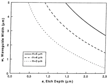
Using single mode conditions given above is not very practical when fabricating waveguides. So, we have reorganized the relations for definite rib heights, H , which is fixed with the silicon top layer for the SOI structure and obtained a plot of controlled fabrication parameters, waveguide width, w and etch depth, e (see Fig.2.8). These are the H values of the SOI structures we used in realization of the devices presented in this work. The areas remained under the plot lines defines the single mode region and the rest remains as multimode region, also due to Eq. 2.21, etch depths can not exceed half of the H values.
Actually, the rib waveguide treatment can be made more realistic by considering the sloped walls formed during chemical wet etching. In this treatm ent, the sloped edges can be approximated by a staircase function of definite number of stairs, and the eigenvalue equation is solved and cut off widths are calculated by the help of an computer p r o g r a m , i n an effectively long and complex manner. Our SOI waveguides are also fabricated by an wet etch process which yields sloped walls of 54.7°, but we prefer to use the EIM analysis explained above, due to its reasonable accuracy and practical simplicity. The single mode
Figure 2.8: Single Mode Condition for rib waveguides with H=3,4and 5 ¡xm. condition will be compared with the BPM simulations and experimental results in Chapter 4.
2.3 Loss in Optical Waveguides
Integrated optical devices are designed to have low power consumption, high speed, size compatibility, low cost, and low loss. Low loss or low attenuation may be the most important concept among all. Characterizing a waveguide means loss measurement after mode analysis of the waveguide. Light reduces in power as it propagates in the waveguide. Power decrease is due to several mechanisms. Power loss in a waveguide is expressed in terms of dB/cm where dB is defined as;
p.
Power{dB) = 10logio{-^^) (2.23)
out
CHAPTER 2. THEORETICAL CONSIDERATIONS 23
2.3.1
Optical Waveguide Loss Mechanisms
Scattering Losses
Two types of scattering losses are under consideration, volume scattering and surface scattering. The former, volume scattering, depends on the number ar.d relative size of imperfections in waveguide material with respect to light wavelength. These imperfections are voids, crystalline defects and contaminant atoms. These imperfections are generally smaller than the wavelength and smaller in number, so volume scattering is not a main scattering mechanism for SOI optical waveguides.
Surface scattering can be an important source of loss and should be reduced during fabrication. Since, light reflects many times from surfaces of a waveguide, it has been showed quantitatively that the surface scattering loss depends on ratio of the roughness of the waveguide surfaces to the wavelength directly, and the waveguide thickness and the amount of the tail of the evanescent field. In the case of the SOI rib waveguides the roughness of the buried Si02 layer, the thickness variation of the top silicon layer and the roughness of the walls of the etched rib are the points to be considered. The first two are related with the fabrication of the SOI substrate and they are results of the optimized commercial technologies. The last is related with the etching of silicon during fabrication process, which was our first task to deal with.
Absorption Losses
This is a mechanism which is mainly important for semiconductor waveguides and is no so important in amorphous thin films and in crystalline ferroelectric materials. Band edge absorption and free carrier absorption are the two types of absorption loss mechanisms that are dominant in semiconductor waveguides like SOI waveguides.
Photons with energy greater than the bandgap energy is absorbed in semiconductors, and the energy of the photon leads valence electrons to be excited to the conduction band. This is a very strong effect. Silicon has a indirect band
gap with 1.1 eV (0.9 /xrn in wavelength). So, we do not have to worry about this loss mechanisms since the wavelength employed in the telecommunication are 1.3 and 1.55 fixn, well apart from the band gap of the silicon.
Free carrier absorption is intraband absorption. A photon gives its energy to an electron in the conduction band exciting it to a higher energy level. This effect is strong when the number of free carriers (electrons and holes) is large. This absorption can be eliminated by utilizing substrates with low doping levels. Low doping levels means small number of free carriers and this means high resistivity. We eliminate this effect for SOI waveguide using wafers with silicon top layers having high resistivity.
Radiation Losses
Actually, the scattering loss is also a radiation loss, that is guided light is somehow leaked into either substrate or cladding and not guided anymore. However, radiation loss is the loss taking' place when the waveguide design is near or beyond cutoff. Well confined single mode waveguides do not suffer significantly from this loss mechanism. However, it is important for multimode waveguides and bending waveguides. In case of SOI rib waveguides, radiation losses are not so significant as long as the waveguide is designed as a single mode waveguide away from the cutoff and the input light is well coupled into the waveguide facet so that slab modes would not be excited.
2.3.2 Measurement of Optical Waveguide Losses
To measure the loss, the simple and straightforward way is to input some light with known optical power into the one facet of the waveguide and measure the optical power at the other facet of the waveguide. Some problems arise when this method is applied. First of all this is not an efficient way for the loss measurement of slab and other multimode waveguides, since individual mode losses can not be determined by this method. Prism-coupling loss measurement technique is preferred for multimode waveguides since it allows measurement of loss for each
CHAPTER 2. THEORETICAL CONSIDERATIONS 25
mode.^ Another problem is that the losses at the input and output ports during coupling can not be known exactly. Despite its drawbacks, this technique is used for determination of losses in single mode waveguides. There are two ways of applying this technique called end-fire coupling(and/or but-coupling) and Fabry- Parot resonance techniques which are explained below.
End-Fire and Butt Coupling
In end — fir e coupling technique, which is the simplest of all, the light with a known wavelength and optical power is focused into cleaved or polished input face of a waveguide using a microscope objective and the transmitted power is measured at the output port. This measurement is repeated for a large number of waveguides having diff'erent lengths, but otherwise identical. This task is accomplished by starting measurements with a relatively long (e.g. several millimeters ) waveguide sample then repetitively shortening the sample by cleaving, or cutting and polishing and measuring these new waveguides with different lengths. The most important problem of this technique is with alignment which should be optimized for each waveguide - microscope objective pair by maximizing output optical power. Then the logarithm of relative transmission is plotted with respect to waveguide length. The plot is a straight line and its slope gives loss coefficient. This technique is effective for the single mode waveguides which can be easily cleaved to optical quality.
Instead of focusing light by a microscope objective an optical single mode fiber can be butt coupled into the waveguide face. The technique is called butt coupling in this case. End-fire coupling is better than butt coupling because alignment can be easier and better optimized by focusing light with an microscope objective into waveguide facet than directly butt coupling an optical single mode fiber of diam eter nearly 9 p m to a waveguide facet of size about 3x3 All the other procedures for measurement and data analysis are the same for both techniques.
Fabry-Perot Interferometer
If the waveguide for which the loss to be measured has optically cleaved facets, it can be considered as a microscopic Fabry-Perot interferometer with facets as the partially transm itted mirrors of the interferometer. Interference pattern is constructed when the phase of the propagating light in the Fabry- Perot interferometer is changed. Optical phase change in a waveguide can be accomplished in two ways, by either increasing waveguide sample temperature by a few degrees or changing the wavelength of the input light continuously . The second way is relatively easier if a tem perature tuned distributed feedback (DFB) laser is used. When applying this technique the same setup as in the end-fire coupling technique is used, except the output of the detector should be visualized graphically to identify the minimums and maximums of the fringes. An oscilloscope or an computer connected optical powermeter or even multimeter would help.
The ratio of the maximum transm itted optical intensity to minimum intensity can be defined as
(1 - Re~°‘^ f
,-aL\2
(1
-in terms of the facet reflectence, R, loss coefficient, a and waveguide (Fabry-Perot cavity) length, L. Defining this ratio as k, the loss coefficient can be stated as
^ ; ro V^·*· (2.25) Using the Eq. 2.25, the optical loss for a waveguide can be determined in one measurement if the facet reflectance is known. In practice the same optical quality can not be repeated in each cleavage of a waveguide sample so the reflectance of the facets can not be known exactly. In th a t case, the same procedure applied in end-fire coupling technique can be employed here. That is, measuring maximum and minimum intensity for waveguide samples with the same features except different lengths. Then, 10/op[(l + v ^ / ( l “ \/^)] which has dimension of dB, versus waveguide length is ploted. This plot will be a straight line. The slope
CHAPTER 2. THEORETICAL CONSIDERATIONS 27
gives optical loss coefficient and extrapolated value to L=0 defines reflectivity of facets.
These techniques can be utilized in optical single mode waveguide loss characterization as long as their limits are considered. Fabry-Perot interferometer technique should be preferred if the waveguides can be cleaved to optical quality. Since it gives directly the total losses explained in this section earlier. This total loss is called propagation loss. The end-fire coupling gives a loss value in which the so-called insertion loss is included. The insertion loss arises from the mismatch between waveguide modes and the light at both input and output ports. This loss has nothing to do with the waveguide material or fabrication quality and it depends on the size of the waveguide, quality of cleaving or polishing and the optimization of the alignment. In the literature end-fire and butt coupling have been reported to be used in SOI waveguide loss characterization mainly.
2.4 Optical Waveguide Directional Couplers
Optical tunneling is responsible for the coupling of optical power from one waveguide to an other one. The device composed of this pair of waveguides is called a waveguide coupler in general and directional coupler if the power exchange happens in a coherent fashion so th at the direction of propagation does not change. Directional couplers are one of the fundamental waveguide devices used in integrated optic circuits. They have been used in circuits designed for power splitting, modulation or switching of light signals, wavelength filtering and polarization selecting.
A directional coupler consists of two identical waveguides very closely placed, as in Fig.2.9. The light incident at input of one of the waveguides couples to the other as it propagates and full coupling of the optical power is possible for long enough coupling length.
In integrated optics, coupled mode formalism is used to treat directional couplers. Coupled mode theory is the theory describing the power exchange between all the optical modes. W hat happens when coupling occurs is that the
Figure 2.9: Schematic layout of a directional coupler
electromagnetic field of waveguides in a directional coupler is not ideal anymore when there is light propagating in adjacent waveguide. Rather it is perturbed
)
by the evanescent tail of the adjacent waveguide. The coupled mode theory describes this perturbed field by superposition of unperturbed or ideal modes of the waveguide. The basic coupled mode theory is based on the scalar wave equation. The advanced couple mode theories based on vector wave equation is still a developing topic. W hat is computed at the end is coupling coefiîcient, k,
for a definite directional coupler design. Knowing k, the exact coupling length
can be determined.
We will demonstrate the coupled mode theory approach for a directional coupler with rib waveguide structure, but the results can be applied to directional couplers with other rectangular waveguide structures by only replacing the refractive indices shown in Fig.2.10 with appropriate ones for each.
This coupled mode approach is also known as degenerate mode coupling, since both waveguides(A and B in Fig.2.10) have the same transverse and longitudinal wavevectors, ac^, Ky and propagation constant, !3. The electric fields in waveguide
A and B are
CHAPTER 2. THEORETICAL CONSIDERATIONS 29
Figure 2.10: Cross section of a rib waveguide directional coupler(a) and its EIM counterpart (b)
EB( x , y , z ) — B cos(Kjjy + (py) cos{kx/2{x - {w + g)))e (2.27) Now, the perturbation made by the evanescent tail of the mode of waveguide A in waveguide B, which is called polarization perturbation, can be written as
Ppert{x,y,z) = € o { n l f f ^ { x , y ) - n l f f2)EAix,y)
(2.28) Only the modes in the same direction will couple to each other, that is there will be no coupling to the backward mode of the waveguide B. Therefore, the amplitude equation of motion will be given in terms of forward mode of B as
dz i 2oj dP i<jJ foo I £b(S^·, y^PpertdS J s ^ Q { n l f f i { x , y ) - n l f f 2 ) s B { x , y ) '00 + c.c.)dxdy = + c.c. (2.29)
where «, the coupling constant, is defined by the integrals and all the constants. There is also a relation similar to the one in Eq. 2.29 for the coupling from waveguide B to waveguide A. These both relations reduces to
9A . „
& =
f - =oz
(2.30)
(2.31) since exponential terms cancel out for the same /?’s. These are strongly coupled differential equations and must be solved simultaneously. Substitution of derivative of Eq. 2.30 into Eq. 2.31 results in
&^A
= -K ^A (2.32)
a second order differential equation, which can be easily solved for initial conditions, .4(0) = 1 and 5(0 ) = 0 to give
A{z) = cos(/c2:)
B{z) = —i sin{Kz) (2.33) As seen in Fig.2.11, the total power goes back and forth between two waveguides and the driven field (waveguide B) always lags 90°. Using the results in Fig.2.11 gives L as
, 7T an
(2.34) then complete energy transfer happens if q is integer, and the length for q=0 is called coupling length and represented by Lc- q values other than integers produce couplings between 0 and 100 percent, k and Lc strongly depends on
^,the gap between waveguide pairs, w, the width of waveguides H, the waveguide (rib) height, h, the waveguide slab height and the refractive index difference between guiding layer and substrate.
CHAPTER 2. THEORETICAL CONSIDERATIONS 31
Figure 2.11; The po\yer exchange between waveguide A and B
Coupled mode formalism is not practical when a directional coupler is designed. As can be seen in the Fig.2.9, waveguides must be bend apart to decouple them at the output. As practical coupling also takes place in this region they bring further complexity to the analysis. They cause radiation loss(as stated in previous section) and change the effective coupling constant and Lc- For this reasons beam propagation method(BPM) has been used in our directional coupler analysis. A commercial BPM based computer program, named B eam P rop has been used to simulate directional couplers. An available mask design was applied to some SOI single mode waveguide structures, then coupling lengths were deduced from these simulations. Simulation results will be given along with optical measurement of fabricated couplers in Chapter4.
2.5
Optical
Multi-Mode Interference (MMI)
Couplers
Multimode interference (MMI) couplers are based on the s el f — imaging
property^^ of multimode waveguides by which an input field profile is reproduced
in single or multiple images at periodic intervals along the propagation direction of the input field. A MMI coupler or power splitter is composed of an central multimode -waveguide that can support a large number of modes (typically larger than 3), N input and M output access waveguides which are usually singlemoded. This is why these devices are also called as N x M M M I couplers. Some examples of MMI couplers are presented in Fig.2.12. MMI couplers have been strong alternatives for its competitors, directional couplers, adiabatic X and Y junction splitters and diffractional star couplers with their high tolerance to polarization and wavelength variations(higfi bandwidth), acceptable fabrication tolerance, low access losses and ability to split light to ports of any number.
Figure 2.12: Some MMI coupler examples
Self-imaging has been known and studied for a relatively long time.^® However, the realization of MMI couplers have been started since the beginning of 90‘s.^® Several analytical analysis methods of the MMI efliect and couplers based on this effect are available. However, we have made use of a mode propagation
CHAPTER 2. THEORETICAL CONSIDERATIONS 33
method based on effective index (2D) approximation which is explained in detail in r e f e r e n c e U s i n g results of this method as a starting point, we designed the MMI couplers to their final version using BPM simulations. A brief summary of the method will be discussed for the sake of the completeness. The detail of our MMI couplers mask design with their BPM analysis results will be presented in Chapter 4 where the results are compared with measurements.
w,
M M Iw,
MMIFigure 2.13: Lateral modes in a multimode waveguide with metal(a) and semiconductor(b) walls
For mode propagation analysis, modes of the multimode waveguide should be determined. For a multimode waveguide of width ridge refractive index, n^ and cladding refractive index , ng there are m lateral modes at the wavelength Aq. The dispersion equation for these lateral modes can be written as
k l + ^ l = kln2^2 r (2.35) for which V.XU is defined as the lateral wave number for mode u and can be find by assuming metal MMI walls. As seen in Fig. 2.5a, metal walls require the fields vanish at the boundaries, which result in standing waves with u nodes for the mode u. From the examples in Fig.2.13a, we can write