1
New Strategies for Defect Passivation in High-Efficiency Perovskite Solar Cells
Seckin Akin, Neha Arora*, Shaik M. Zakeeruddin,Michael Grätzel, Richard H. Friend, M. Ibrahim Dar*
Dr. N. Arora, Dr. M. I. Dar, Prof. R. H. Friend
Cavendish Laboratory, Department of Physics, University of Cambridge, JJ Thomson Avenue, Cambridge CB3 0HE, UK
E-mail: [email protected], [email protected]
Dr. S. Akin, Dr. S. M. Zakerruddin, Prof. M. Grätzel
Laboratory of Photonics and Interfaces, Department of Chemistry and Chemical Engineering, École Polytechnique Fédérale de Lausanne, Lausanne CH-1015, Switzerland
Dr. S. Akin
Department of Metallurgical and Materials Engineering, Karamanoglu Mehmetbey University, 70100, Karaman, Turkey
Keywords: (perovskite solar cells, defects, passivation, efficiency, mixed-cation-halide, 2D-3D, engineering, stability)
Lead halide perovskite solar cells (PSCs) now show excellent efficiencies and encouraging levels of stability. Further improvements in performance require better control of electron-hole recombination processes associated with trap states. Such trap states are considered to be associated with vacancies and defects at crystallite surfaces. We consider here how these traps can be mitigated by improving the quality of the perovskite layer and interfaces in fully assembled device configurations. In this review, we discuss most recent design strategies reported in the literature, that have been explored to tune grain orientation, to passivate defects, and to improve charge-carrier lifetimes. Specifically, we discuss advances made with single-cation, mixed-cation, and mixed-halide, and three-dimensional/two-dimensional- (3D/2D) bilayer based light absorbers. We focus on interfacial, compositional, and band alignment engineering with their consequent effects on the open-circuit voltage, power conversion efficiency, and stability.
2
1. Introduction
The impetus to commercialize lead-halide perovskite solar cells (PSCs) as next-generation solar cells arises from their simple and facile solution-processibility.[1,2,3,4,5] In addition, their desired optoelectronic properties such as high absorption coefficient with long carrier
diffusion lengths have promoted the research domain targeting low-cost and high-efficiency solar cells. [6,7,8,9] Initially, Miyasaka and co-workers reported breakthrough research on liquid electrolyte based PSCs with power conversion efficiency (PCE) of 3.8% in 2008.[10]
Subsequently, higher PCEs were obtained while employing spiro-OMeTAD, a solid-state hole conductor in PSCs.[4,6] All-solid-state PSCs also revealed that the generation of free-charges inside the bulk of the perovskite absorber layer. Since then, the PSC research field has expanded dramatically with PCEs exceeding 25%.[11] One of the important aspects of
improving the PCE of PSCs is to minimize non-radiative recombination processes and preclude the carrier quenching both within the photoactive layer and at the interfaces while simultaneously promoting balanced charge transport and collection.[12,13,14,15]
Although it is difficult to know the nature of defects and to differentiate defects located at the surface and grain boundaries (GBs), their formation could be finely controlled by controlling the growth and morphology of the perovskite films and other structures.[16,17,18]
In addition, the compositional engineering of these ABX3 compounds, which allows tailoring
of the bandgap, could be explored to improve the optoelectronic properties with great rationality to simultaneously increase the efficiency and stability of PSCs. Recently, many advances in the compositional (cation and/or anion) engineering including the partial substitution of formamidinium (FA+) cation and I-, respectively, with methylammonium (MA+) and Br- have been made to enhance both performance and stability.[19,20] In addition,
3
(Na+), silver (Ag+), guanidinium (Gua+) have been explored into the perovskite films to enhance the photovoltage (VOC) of PSCs.[21,22,23,24]
The mitigation of instability issues, which get aggravated in the presence of traps, is one of the main challenges that PSCs technology is facing currently. Therefore, it has become imperative to passivate defects located at the surface and GBs.[25,26] Towards this end, various strategies such as interface engineering via surface passivation and charge compensation by using metal oxides, additive engineering approach, which was employed to enlarge the dimensions of perovskite grains, and to increase the crystallinity, and small molecules, or polymers etc. have been developed for the stabilization of crystal phase and defect management in PSCs. [27,28,29] More recently, the application of 2D Ruddlesden–Popper layered perovskites (RNH3)2(A)n-1BX3n+1), (n = 1, 2, 3, 4,. . ∞) (where n is the number of
layers and RNH3 are large alkyl ammonium cations) have been proposed as stable alternatives
to 3D perovskites because of their superior hydrophobicity and thermostability.[1, 30,31] However, the PSCs employing 2D perovskites as the active layer display relatively poor performances primarily due to the anisotropic transport properties, which are intrinsically associated with the layered structure. Interestingly, in conjugation with the 3D perovskites, both efficiency and stability can be synergistically improved mainly due to the passivation of interfacial GBs in a 3D/2D bilayer configuration.[1] Such a bilayer architecture also minimizes the issues associated with the hygroscopic nature of the 3D-perovskite material and sensitivity towards high temperature, which can induce the degradation of the interfaces and rapidly decrease the photovoltaic performances within a short period of operation. The graded combination of 2D/3D can also hinder the ionic-motion and mitigate the parasitic interfacial charge-carrier recombination.[32]
4
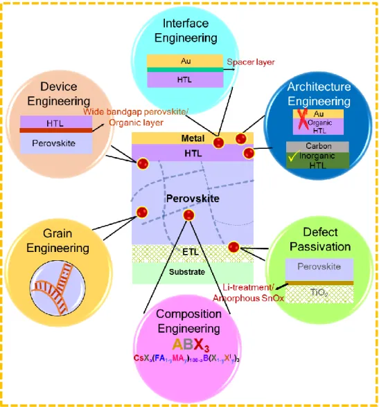
Figure 1. Schematic illustration of different passivation strategies for high-efficiency
perovskite solar cells.
In this review, we provide an overview of the recent progress on the strategies adopted to passivate defects to realize high-efficiency PSCs (Figure 1). Firstly, we aim to highlight the routes that have been successfully explored to control the non-radiative recombination and enhance the photovoltage of PSCs. Specifically, most recent reports on PSCs based on single-cation to mixed-single-cation and/or mixed- halide to the 3D/2D perovskite system will be
discussed. The next section illustrates the stability of the PSCs based on these systems probed under illumination, humid conditions and thermal stress. Finally, the last section will provide the perspectives about this enticing scientific domain, i.e., defect passivation in PSCs.
5
2. Single cation-based perovskites
In the last decade, PSCs has become a promising and emerging technology with certified efficiency exceeding 25%,[11] This photovoltaic technology began with PSCs involving
single-cation based light absorber with an efficiency of 3.8%.[10] The forthcoming sections highlight recent reports showing that the approaches including composition-additive, charge transport layers, interface, and device architecture engineering are critical to the performance of these single cation-based PSCs.
2.1. Composition-additive engineering in single cation perovskites
A high-quality perovskite film with low-amount of grain boundaries and fewer trap states in the bulk and/or at the interfaces is necessary to obtain good performance.
Composition-additive engineering is one of the most efficient strategies to obtain perovskite films with high crystallinity, smooth surfaces, and large grains, which reduce the grain boundaries and trap states. In this section, composition-additive engineering approaches for single-cation perovskite absorber are discussed.
Carmano et al. fabricated the n-i-p-type mesoporous PSCs based on a
non-stoichiometric PbI2: MAI ratio (x: 1, being x ≥ 1) in the perovskite precursor solution.[33] The
obtained results demonstrated that the unreacted PbI2 enhances the crystallinity of the
perovskite film due to the stronger interfacial coupling at the interface and promotes the electron transfer from perovskite to TiO2 layer owing to better band alignment. As a result of
these remarkable properties, an improvement in the FF and VOC (as high as 1.11 V) was acquired, boosting the averaged PCE from 16.2% to values close to 18%, with a champion efficiency of >19%. It is worth mentioning that the concept of using excess PbI2 renders the
use of precursors containing a stoichiometric ratio of PbI2: MAI undesired, as was commonly
believed in the PSC field. In some cases, different methodologies were introduced to induce rapid crystallization of the perovskite structures with a slight excess of PbI2. For example,
6
laser irradiation was explored to obtain homogeneous and dense-grained MAPbI3 films.[34]
The advantage of laser irradiation is to produce a thermal gradient, which was found to be beneficial for the formation of the desired amount of PbI2 on the surface of CH3NH3PbI3
perovskite film. Consequently, the parasitic recombination occurring at the interface decreased due to self-passivation, minimizing the voltage loss to 0.41 V.
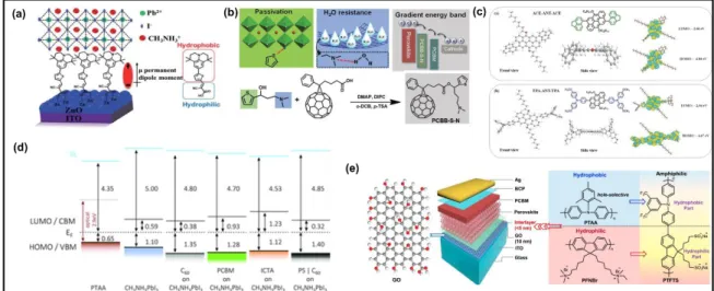
New molecules were also designed to passivate the defects (defect-healing), which greatly improved the efficiency and stability of PSCs. Zheng et al. reported a study to
passivate the ionic defects at the surfaces and grain boundaries of MAPbI3 perovskite films by
using quaternary ammonium halides (QAHs), i.e., 𝑁𝑅4+𝑋−(𝑅 is an alkyl or aryl group and 𝑋 is halide).[35] In addition to a significant reduction in the trap-state density, an improvement in
the charge carrier lifetime was also observed in the presence of choline chloride-based
passivation layer as shown in Figure 2a. As a result of successful passivation of ionic defects, the VOC of the p-i-n-architecture based planar devices increased from 1.04 V to 1.15 V with a significant enhancement in PCE (17.1% to 20.0%) and hysteresis-free behavior. In addition, the defect healing approach enhanced the ambient stability of the perovskite films. The larger VOC yielded by the devices involving choline chloride QAHs was attributed to their
zwitterionic structure and to the additional passivation effects of the halide ions (Figure 2b). Another interesting aspect related to additive engineering approach is to achieve high-quality perovskite absorber films. For example, Wu et al. demonstrated that the addition of a small amount of H2O into PbI2/DMF makes a homogenous precursor solution for depositing
high-quality PbI2 film in a two-step method.[36] Apparently, moisture can assist the grain growth of
the perovskite film to improve the charge-carrier lifetime and carrier mobility.[37] In this
study, highly pure, smooth, crystalline and oriented perovskite films were deposited on PEDOT:PSS surface. The PbI2 film involving 2 wt% water exhibited the smoothest and
7
densely packed films composed of large grains. The inverted-type champion PSC showed a remarkable FF of 0.85, resulting in a PCE of 18% with a VOC of 1.03 V.
Recently Han et al. developed an additive-based room temperature process to obtain high-quality MAPbI3 films with micron-sized grains (>2 µm), employing a simple
low-vacuum process.[38] Authors used methylammonium thiocyanate (MASCN) as an additive and achieved microsecond-range carrier lifetimes and highly crystalline perovskite films at room temperature. As a result of these excellent film characteristics, the best PCE of 18.22% (average 16.92%) with low hysteresis and respectable environmental stability under the standard illumination was realized, whereas the control device (without additive)
demonstrated only 2.04% PCE with JSC of 8.78 mA cm-2, VOC of 0.638 V and FF of 0.36, under similar conditions. Such an improvement in the photovoltaic parameters was explained on the basis of increased grain size and improved crystallinity of perovskite films. The additive-based mechanism was proposed and verified by Tindall-effect tests and DLS measurements. The coordination of SCN- with Pb2+ facilitates enlargement of the precursor
aggregates up to microscale before spin coating which arranges in an ordered fashion on the substrates during the film deposition. The solvent and volatile SCN- were removed by applying low-vacuum as depicted in Figure 2c.
Very recently, Zhou et al. employed the imidazole sulfonate zwitterion, 4-(1H-imidazol-3-ium-3-yl) butane-1-sulfonate (IMS), as a bifunctional additive in an n-i-p planar MAPbI3 based type PSCs.[39] It was reported that this additive not merely arranges the crystal
orientation but also passivates the trap states of MAPbI3 perovskite film especially the iodine
vacancy. The effect of bi-functional IMS additive observed due to coordination between sulfonate moiety of IMS and Pb2+ ion as well as electrostatic interaction between imidazole of IMS and I– ion of perovskite (Figure 2d). As a result, the PCE and Voc increased from
8
presence of 0.5 wt% IMS doping. For a 1.2 wt% IMS doping ratio, a VOC of 1.208 V was achieved, and this was claimed to be the highest VOC for MAPbI3 employing n-i-p structured
planar PSCs.
A record VOC of 1.26 V has been demonstrated for planar solar cells with inverted architecture based on smooth MAPbI3 perovskite films with large grains.[40] The perovskite
films were obtained after employing the combination of lead acetate (PbAc2) and lead
chloride (PbCl2) precursors and optimizing the contact layers. In addition, exceptionally long
photoluminescence lifetimes, which translated into a magnificent PCE of ∼20.7% were reported.
In addition to the molecular doping, the introduction of metal ions in the perovskite structure is another promising approach to address the main critical concerns of PSCs.
Towards this end, various monovalent cations including Na+, Ag+, Cu+ were introduced in the
MAPbI3 films to improve the optoelectronic properties of MAPbI3 structures, [41,42] which
consequently increased the photovoltaic performance of the resulting devices. The role of other inorganic cations such as Cs+ and Rb+ was also investigated in various perovskite
compositions and the insights gained through various structural, thermal and spectroscopic studies amply established the absence of Rb+ whereas, under similar conditions, a certain
amount of Cs+ was found to be occupying the A-site in 3D perovskite.[43] In another interesting study, Pb metal in MAPbI3 perovskite films was substituted by nine different
alternative divalent metal species such as Co, Cu, Fe, Mg, Mn, Ni, Sn, Sr, Zn to screen the tolerance of perovskite film towards extrinsic homovalent metal species and its impact on the photovoltaic performance of inverted-type MAPbI3 PSCs.[44] It was proven that the MAPbI3
film shows a much higher tolerance without any performance loss in comparison to crystalline silicon when less than 3% of the Pb2+ ions were replaced. This compositional engineering approach also showed that not only well-known Sn2+ but also Co2+ can replace Pb2+ from the
9
perovskite lattice as revealed by the crystallographic analysis. By using the optimum molar ratio of 63Pb:1Co, the best PCE of 17.2% with an improved VOC (from 0.96 V for the
baseline to 1.05 V for 63Pb:1Co and to 1.08 V for 31Pb:1Co ratio) over the standard MAPbI3.
The ~120 mV increase in VOC was attributed to the ability of Co2+ to shift the Fermi level and
valence band edge of the perovskite material into a more favourable energetic alignment with HTL. Apparently, the obtained results showed that transition metal substitution could provide a new dimension for tuning the electronic and crystallographic properties of perovskite films while maintaining high photovoltaic performance.
Figure 2. a) Charge carrier lifetime curves of control and choline chloride-treated devices,
estimated from transient photovoltage measurement under open-circuit conditions.
Reproduced with permission. [35] Copyright 2017, Nature Publishing Group. b) Schematic illustration of quaternary ammonium halides assembled on the defect sites (the red and blue symbols represent the N and O atoms of the choline chloride molecule, respectively). Reproduced with permission.[35] Copyright 2017, Nature Publishing Group. c) Schematic flow diagram of the room-temperature process to deposit MAPbI3 films and proposed film
formation mechanism. Reproduced with permission.[38] Copyright 2017, Royal Society of Chemistry. d) Proposed formation mechanisms of MAPbI3 perovskite structure a) without and
b) with imidazole sulfonate zwitterion, 4‐(1H‐imidazol‐3‐ium‐3‐yl)butane‐1‐sulfonate (IMS), as a bifunctional additive. Reproduced with permission.[39] Copyright 2019, John Wiley & Sons.
In this section, we have covered recent reports of photovoltage enhancement in single-cation based PSCs in the context of composition-additive engineering. Quiet versatile
10
methods have been discussed including defect healing, increase in grain size and introduction of metal ions in the perovskite absorber. In the following, the different methods for energy band-alignment and interface engineering resulting in the improvement of photovoltaic parameters will be discussed.
2.2. ETL engineering in single cation perovskites
The electron transport layers (ETLs) play an indispensable role in PSCs owing to their key electron extracting/transporting features. Although TiO2 is considered as the most promising
ETL material for highly efficient PSCs, it needs to be modified using suitable approaches or replaced with better alternatives to combat the current challenges, i.e., low electron mobility, insufficient band-offset, and high sintering temperature. In this section, highly promising modification methods and alternative ETL materials are presented to illustrate the importance of ETL materials in the state-of-the-art PSCs based on the single-cation absorber.
The impact of magical TiCl4 treatment was unraveled using photothermal deflection
spectroscopy (PDS), and results amply showed a decrease in the energetic disorder not merely in mesoporous TiO2 but also in CH3NH3PbI3 light absorber layer.[45] Using [6,6]-phenyl-C61
-butyric acid (PCBA) monolayer modified compact TiO2 (c-TiO2) substrates, high-quality
CH3NH3PbI3 films were deposited for planar heterojunction PSCs.[46] The PCBA interfacial
layer reduced the hole recombination by acting as the hole blocking layer at the
c-TiO2/CH3NH3PbI3 interface and facilitating efficient electron extraction by the ETL. The
formation of a chemical bond between c-TiO2 and the carboxyl group of PCBA as well as the
low solubility of PCBA in perovskite solvent of N, N-dimethylformamide (DMF) helped to obtain pin-hole free perovskite films, resulting in significant enhancement of photovoltaic performance from 7.46% to 13.33%. The best PCE of 17.76% with an outstanding VOC of 1.16 V was achieved by optimizing the perovskite thickness.
11
Miyasaka and co-workers developed a fully low-temperature-processed PSCs
employing an ultrathin amorphous TiOx ETL in combination with brookite TiO2 prepared at
<150 °C.[47] The TiOx/brookite TiO2 bilayer ETL based PSCs demonstrated an excellent PCE
up to 21.6%, supported by a remarkable VOC and FF of 1.18 V and 0.83, respectively, as a result of well-matched band alignment with respect to brookite TiO2. The authors also
examined SnOx as an alternative ETL to TiOx in combination with brookite TiO2. Although
the SnOx/brookite TiO2 bilayer ETL based PSCs yielded VOC and JSC as high as TiOx/brookite
TiO2 based PSCs, loss of FF resulted in relatively lower PCE. The electron band edge
potentials of ETLs and brookite TiO2 were evoked to explain the drop in FF, whereas more
negative conduction band edge of SnOx exhibited an energy barrier for electron injection from
brookite TiO2 into SnOx layer.
In comparison to TiO2 and SnO2, ZnO exhibits more promising electron extraction
ability owing to its superior electron mobility and more favourable band-offset. A simple strategy was developed to obtain planar PSCs at low-temperature by combining bi-functional self-assembled monolayer (SAM)-modified ZnO electron-accepting layers with sequentially prepared perovskite active layers.[48] Highly polar molecules of bithiophene conjugated cyanoacrylic acid (T2CA) julolidine moiety conjugated cyanoacrylic acid (JTCA) were employed as the SAM as shown in Figure 3a. The JTCA-modified ZnO ETL based PSCs reached a PCE of 18.82% with VOC of 1.13 V, whereas the pristine ZnO ETL based PSC reached only 15.41% with VOC of 1.06 V. The trap state measurements showed a lower trap density in the JTCA (SAM)-modified device whereas the carrier mobility of the ITO-JTCA employing device was 50% higher (0.61 cm2 V−1 s−1) than that of bare ITO (0.43 cm2 V−1 s−1).
A large enhancement in the VOC from 0.962 V to 1.135 V and PCE from 14.15% to 19.14% was reported for PEDOT:PSS HTL based inverted type MAPbI3 based PSCs by employing
12
interface and MoS2 at PCBM/Ag interface.[49] The VOC was further improved to 1.176 V when
the perovskite structure was doped with Br- (MAPbI
2.5Br0.5). In addition to enhanced ohmic
contact, which facilitates the rapid transfer of the electrons across the MoS2/Ag interface,
MoS2 layer also showed a hole blocking potential to decrease the recombination at the
interface near the cathode. The combination of energy level matching at the contact interface and the electronic and chemical properties of the 2D materials resulted in the improvement of photovoltaic parameters. The enhancement in the device stability was also reported in the presence of interlayers due to the blocking of the ion diffusion at the PEDOT: PSS/perovskite and PCBM/Ag interfaces.
More recently, a hydrophobic fullerene derivative, [6,6]-phenyl-C61-butyric acid-N,N-dimethyl-3-(2-thienyl)propanam ester (PCBB-S-N) containing a functional sulphur atom and C60 was synthesized and employed as an intermediary layer on PCBM ETL to heal the
defect states in PSCs (Figure 3b).[50] The resulting planar p-i-n MAPbI3 PSCs exhibited
much-improved PCE of over 21% relative to bare PCBM ETL-based control device (PCE 17.41%), and also showed excellent moisture and thermal stability. The enhanced VOC of 70 mV was attributed to the slightly increased LUMO energy level of PCBB-S-N and passivation of antisite defects by the pendent thiophene moieties, while higher FF and JSC values were explained on the basis of formation of compact and homogeneous PCBB-S-N film
contributing to its electronic contact with the cathode.
2.3. HTL engineering in single cation perovskites
Despite playing a key role in PSCs, the high cost of spiro-OMeTAD is an issue. Moreover, spiro‐OMeTAD can easily provoke the degradation of perovskite structure upon thermal stress and at perceived humidity levels owing to its amorphous and highly hygroscopic nature. The following section introduces the alternative HTL materials and an outline of current
13
routes, which were employed to enhance the photovoltaic performance of the devices based on MAPbI3 absorber.
Bi et al. investigated the grain growth of MAPbI3 perovskite for efficient inverted-type
PSCs as a function of wetting-ability of HTLs.[51] To study the effect of the wetting-ability,
MAPbI3 film were deposited on different wetting and non-wetting polymer substrates such as
polyvinyl alcohol (PVA), poly(3,4-ethylenedioxythiophene) polystyrene sulfonate (PEDOT: PSS), crosslinked N4,N4′-bis(4-(6-((3-ethyloxetan-3-yl)methoxy)hexyl)phenyl)-N4,N4′-diphenylbiphenyl-4,4′-diamine (c-OTPD), poly(bis(4-phenyl)(2,4,6-trimethylphenyl)amine) (PTAA), and poly(N-9′-heptadecanyl-2,7-carbazole-alt-5,5-(4′,7′-di-2-thienyl-2′,1′,3′-benzothiadiazole)) (PCDTBT). The wetting capability of the different substrates was
determined by contact angle measurement and the values of 10o, 12o, 79o, 105o and 108o were obtained for PVA, PEDOT: PSS, c-OTPD, PTAA, and PCDTBT, respectively. SEM images indicated that the average MAPbI3 grain size (apparent) on c-OTPD (480 nm) is much larger
than that on PEDOT: PSS (230 nm). This result indicates that a non-wetting surface can suppress the heterogeneous nucleation and facilitate grain boundary migration, resulting in low nucleation density and thus larger grain size. As a result of the reduced grain boundary area and dramatically improved crystallinity, a significant reduction in the charge
recombination and charge trap density by 10–100-fold was achieved.
Pham et al. presented highly efficient and humidity-resistant PSCs by using two new small molecule-based HTLs, i.e, anthanthrone (ANT) dye, namely,
4,10-bis(1,2-dihydroacenaphthylen- 5-yl)-6,12-bis(octyloxy)-6,12-dihydronaphtho[7,8,1,2,3-nopqr]tetraphene (ACE-ANT-ACE) and
4,4′-(6,12-bis(octyloxy)-6,12-dihydronaphtho[7,8,1,2,3-nopqr]tetraphene- 4,10-diyl)bis(N,N-bis(4-methoxyphenyl)aniline) (TPA-ANT-TPA) (Figure 3c).[52] After extensive optimization in device processing
14
achieved with negligible hysteresis for devices based on dopant-free TPA-ANT-TPA HTL whereas a slightly lower PCE of 13.1% with JSC of 18.7 mA cm−2, VOC of 1.03 V, and FF of 0.67 was recorded for ACE-ANT-ACE based device. The doped spiro-OMeTAD HTL based device showed a PCE of 16.8% with JSC of 21.09 mA cm−2, VOC of 1.04 V, and FF of 0.77. The difference in JSC values for devices based on new HTLs was explained on the basis of the shallower HOMO level of TPA-ANT-TPA that allowed an effective hole extraction. In addition to rapid quenching of PL for TPA-ANT-TPA HTL system, a close alignment of HOMO energy levels with minimal band offset demonstrated the great potential of
corresponding HTL for designing highly efficient PSCs. Because of the hydrophilic nature of the corresponding HTLs, improved stability was reported as compared to hygroscopic LiTFSI doped spiro-OMeTAD.
2.4. Interface engineering in single cation perovskites
Interface engineering is also important to further increase efficiency by improving the charge collection and by reducing the parasitic charge-carrier recombination. The effects of interface engineering on the photovoltaic performance of MAPbI3 based PSCs is presented in the
following section.
Wolff et al. carried out a systematic investigation of the energetics and the VOC losses in MAPbI3 PSCs with different fullerene derivatives (PCBM, C60, and ICTA) employed in the
ETL.[53] The analysis of energetics and the VOC losses demonstrated that PCBM and C60 are
not the ideal ETLs when targeting high VOC. The fabricated devices with ICTA, which has the lowest electron affinity, i.e., the highest LUMO level among the fullerenes tested in this study, exhibited the highest VOC while C60 with the lowest-lying LUMO level showed the
lowest VOC (Figure 3d). The insertion of an ultrathin layer of insulating polystyrene (PS) between the MAPbI3 and C60 increased the VOC by as much as 130 mV (on average 120 mV),
15
electroluminescence (EL) measurement, a better EQEEL was found, indicating that
non-radiative recombination of injected charge becomes progressively suppressed upon lifting the LUMO level, and it was further reduced by inserting the PS layer.
A low-temperature (140 oC) processed SnO
2 was employed as an ETL for MAPbI3
planar PSCs on a flexible PEN (polyethylenenaphthalate) substrate.[54] A C
60 pyrrolidine
tris-acid (CPTA) was used to modify the interface between SnO2 and MAPbI3 to significantly
enhance the photovoltaic performance. This flexible PSC achieved a PCE of 18.36% under simulated AM1.5 sunlight and maintained 75% of its initial efficiency after 500 cycles of bending with a curvature radius of 5 mm. The PL measurements of MAPbI3 film on SnO2
-CPTA substrate showed a 6-fold weaker PL intensity than that of MAPbI3 on pristine SnO2,
indicating the efficient extraction of electrons in the presence of CPTA.
In another interesting work, a new method of fabricating large-area flexible PSCs by inserting a conjugated polyelectrolyte interlayer (PTAA, PFNBr, and PTFTS) between the MAPbI3 and HTL (graphene oxide, GO) was described (Figure 3e).[55] To investigate the
wettability of interlayers on GO layer, the contact angles of perovskite precursor solutions on GO/PTAA, GO/PFNBr and GO/PTFTS of 78°, 21°, and 44°, respectively, were determined, whereas the pristine GO provided a contact angle of 29°. Apparently, non-wetting surface facilities the growth of larger grains due to the dramatic suppression of heterogeneous nucleation. [51] The resulting perovskite film on GO/PTAA showed no pin-holes with an
average grain size of 800 nm, whereas the average size of perovskite grains on GO/PTFTS was ~550 nm. For the best-performing GO-based device, a PCE of 14.91% with VOC of 1.05 V, was reported while a remarkable PCE of 18.82% was achieved for PTFTS-modified GO HTL based devices. The GO/PTFTS (1.09 V) and GO/PTAA (1.07 V) based devices showed a higher built-in potential (Vbi) than pristine GO-based device (0.99 V), correlating with the
16
Figure 3. a) Schematic illustration of SAM-induced permanent dipole moment at the
ZnO/perovskite interface. Reproduced with permission.[48] Copyright 2018, John Wiley & Sons. b) Design and synthesis of PCBB-S-N, with a targeted therapy effect. Reproduced with permission.[50] Copyright 2019, John Wiley & Sons. c) Chemical structures, geometrical configuration (front view and side view), and calculated isosurfaces and energy levels of HOMO and LUMO orbital surfaces of a) ACE-ANT-ACE and b) TPA-ANT-TPA,
synthesized by classical Suzuki coupling. Reproduced with permission.[52] Copyright 2018, John Wiley & Sons. d) Schematic energy-level diagram of the different layers relative to EF.
Reproduced with permission.[53] Copyright 2017, John Wiley & Sons. e) The inverted device architecture of planar-type PSCs and the chemical structures of GO and polymer interlayers. Reproduced with permission.[55] Copyright 2019, Elsevier.
2.5. Other (Architecture) engineering in single cation perovskites
Apart from the above-mentioned engineering strategies, architecture engineering is another promising way to achieve high VOC. Huang et al. designed a novel prismatic PSCs with light trapping configuration to mitigate the losses.[56] In the current system, incident high-to-low energy photons were separately captured by four horizontally aligned MAPbIxBr3-x (x = 3, 2,
1, and 0) sub-cells with varied bandgaps. This approach generated a record VOC of 5.3 V and a significant PCE of 21.3%, Basically, this new form of cell architecture minimized the
thermodynamic losses and improved the photovoltages of PSCs by subsequently harvesting the incident photons with different energies using four different MAPbIxBr3-x sub-cells. As a
result of subsequent harvesting of high-to-low energy photons, the corresponding sub-cells based on MAPbBr3, MAPbIBr2, MAPbI2Br and MAPbI3 absorber layers generated a VOC of
17
1.54 V, 1.45 V, 1.25 V and 1.15 V, respectively, yielding a record VOC of 5.3 V. This study clearly demonstrates that the mitigation of thermodynamic loss and light trapping can be achieved by carefully designing the absorption of active layers to achieve a higher VOC and PCE.
Overall, the highlighted reports in this section of the review show that despite the relatively poor device stability of single-cation iodide-based PSCs, an appropriate engineering approach can dramatically improve not only photovoltaic performance but also operational stability of resulting devices. From this perspective, it is clearly evident from the above-mentioned studies that more efficient charge-transporting layers showing well-matched band alignment with perovskite can be obtained by doping and/or treatment strategies, whereas composition-additive engineering can be readily employed to form a high-quality perovskite layer with fewer trap states in the bulk and/or at the interfaces. Table 1 summarizes the recent progress on the photovoltaic performance of single-cation iodide-based PSCs.
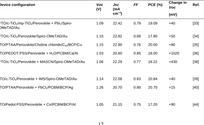
Table 1. VOC and other photovoltaic parameters yielded by single-cation and iodide perovskite-based PSCs.
Device configuration Voc
(V) Jsc (mA cm−2) FF PCE (%) Change in Voc (mV) Ref.
FTO/c-TiO2/mp-TiO2/Perovskite + PbI2
/Spiro-OMeTAD/Au
1.09 22.42 0.79 19.09 +40 [33]
FTO/c-TiO2/Perovskite/Spiro-OMeTAD/Au 1.15 22.82 0.68 17.80 +50 [34]
ITO/PTAA/Perovskite/Choline chloride/C60/BCP/Cu 1.15 22.90 0.76 20.00 +90 [35]
ITO/PEDOT:PSS/Perovskite + H2O/PCBM/Ca/Al 1.03 20.60 0.85 18.00 +1020 [36]
FTO/c-TiO2/Perovskite + MASCN/Spiro-OMeTAD/Au 1.06 22.29 0.77 18.22 +430 [38]
ITO/c-TiO2/Perovskite + IMS/Spiro-OMeTAD/Au 1.14 22.08 0.83 20.84 +40 [39]
ITO/PTAA/Perovskite + PbCl2/PCBM/BCP/Ag 1.26 20.70 0.80 20.70 +15 [40]
18
FTO/c-TiO2/PCBA/Perovskite/Spiro-OMeTAD/Ag 1.16 21.38 0.72 17.76 +80 [46]
ITO/TiOx/brookite TiO2/Perovskite/Spiro-OMeTAD/Au 1.18 21.86 0.83 21.60 +40 [47]
ITO/JTCA-modified ZnO/Perovskite/Spiro-OMeTAD/Au 1.13 21.72 0.76 18.82 +70 [48] ITO/Pedot:PSS/GO/Perovskite/PCBM/MoS2/Ag 1.14 22.83 0.74 19.14 +70 [49]
ITO/PTAA/MAPbI3/PCBB-S-N/PCBM/Al 1.12 23.83 0.79 21.08 +70 [50]
ITO/PTAA/Perovskite/PCBM/C60/Al 1.07 22.00 0.77 18.10 +150 [51]
FTO/c-TiO2/mp-TiO2/Perovskite/TPA-ANT-TPA/Ag 1.03 21.05 0.80 17.50 -10 [52]
ITO/PTAA/Perovskite/PS/C60/Cu 1.16 22.30 0.75 19.42 +130 [53]
ITO/CPTA-modified SnO2/Perovskite/Spiro-OMeTAD/Au 1.08 22.39 0.75 18.36 +30 [54]
ITO/GO/PTFTS/Perovskite/PCBM/BCP/Ag 1.10 20.89 0.82 18.82 +50 [55] FTO/c-TiO2/mp-TiO2/Perovskite/TPA-ANT-TPA/Ag 1.03 21.05 0.80 17.50 -10 [52]
ITO/PTAA/MAPbI3 + PCBB-OEG/PCBM/Al 1.07 23.65 0.80 20.20 +30 [57]
ITO/ZnO/PVP/Perovskite/Spiro-OMeTAD/MoO3/Ag 1.07 19.97 0.56 14.12 +70 [58]
FTO/NiO/CuI/Perovskite/PCBM/BCP/Ag 1.07 20.60 0.69 15.26 +50 [59]
3. Mixed cation and/or mixed halide-based perovskites
The functionality and performance of the perovskite absorber layer are mainly dependent on the chemical composition. Although MAPbI3 perovskite material has been extensively used as
a light-harnesser in device architecture, the best-performing devices use mixed cations and/or mixed halides perovskite absorber. The chemical modification of the X-site anions and A-site cations improved the optoelectronic properties and modulated the device efficiency. For instance, the introduction of formamidinium (FA+) cations into MAPbI
3 structure led to the
fabrication of MA0.6FA0.4PbI3 based PSCs yielding an efficiency up to 14.9%,[60] whereas the
mixed-halide perovskite composition with the substitution of 10-15 mol% of iodide with bromide facilitated a fully solution-processed PSCs with a certified efficiency of 16.2%.[61]
The bandgap of mixed-halide perovskites can be effectively modulated by controlling the composition of incorporated halides, whereas the mixed-cation perovskites can make the halide redistribution thermodynamically unfavorable and consequently minimize the halide
19
segregation. The emerging compositions render these systems enormously appealing for designing of perovskite devices, displaying outstanding efficiency, long-term operational stability, and low process sensitivity. In the following section, we summarize the recent advances in the modification of A-site and/or X-site of the ABX3 perovskite structure (where
A is an organic ammonium cation, B is Pb+2 or Sn+2, and X is a halide anion).
3.1. Composition-additive engineering in mixed-cation and/or mixed-halide perovskites
The overall efficiency and stability of PSCs are strongly dependent on the composition of the perovskite materials. In addition to enhanced device stability and other desirable
optoelectronic properties, the mixed-halide perovskite compositions offer a great opportunity to optimize the spectral range by tuning the bandgap of the corresponding films. The
incorporation of different types of halides into a crystal lattice also lead to radical changes in perovskite morphology, which can further improve the efficiency and stability of PSCs. Initially, the role of chloride remained a mystery, later studies including both electron microscopy-based analysis and bandgap studies clearly brought out that the presence of chloride can influence the growth, morphology and charge-carrier recombination without altering the bandgap of MAPbI3.[62] In a similar direction, bromide was found to play a similar
role, leading to significant improvement in PCE from 14 % to >16%.[17,18,63,64] Highly-efficient PSCs (certified PCE 16.2%) were initially reported for mixed-halide based MAPb(I1−xBrx)3 (x=0.1–0.15) perovskite absorbing layer using solvent engineering
technique.[61] A mixed solvent of γ-butyrolactone (GBL) and dimethylsulphoxide (DMSO)
was used followed by a toluene drop-casting to obtain dense and fully covered perovskite films on the mesoporous TiO2 layer. It was shown that the formation of a stable MAI(Br)–
20
solvent (toluene) was critical in retarding the rapid reaction between MAI(Br) and PbI(Br)2
which enabled the formation of a highly uniform and highly crystalline perovskite films. Recently, Longo et al. fabricated fully vacuum-deposited mixed-halide
methylammonium lead mixed-halide MAPb(BrxI1−x)3 (x = 0.2 and 0.5) perovskite films with a
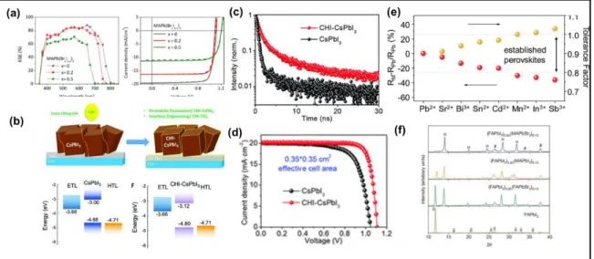
bandgap of 1.72 and 1.87 eV.[65] The photoluminescence (PL) signal did not change under prolonged illumination at low Br– ratio, while halide segregation was observed at high Br– concentrations similar to solution-processed perovskite films. The absorption onset of the obtained films showed a monotonic blue-shift with increasing Br– content. The VOC increased from 1.095 V to 1.119 V to 1.207 V for devices employing perovskite with the Br– the content of x = 0, 0.2, and 0.5, respectively (Figure 4a). The increase in VOC of the corresponding perovskite compositions was attributed to the widening of the bandgap.
The effect of thermal treatment on the intermediate state was also investigated for hydrobromic acid (HBr) assisted fast crystallization process of mixed-halide MAPbI3−xClx
based perovskite films.[66] This approach helped to achieve rapid formation and crystallization
of perovskite films after the annealing step. The enhancement in the device performance was attributed to the increased shunt resistance, lower leakage current, reduced series resistance, and stronger crystallization of the corresponding perovskite layer in the presence of HBr treatment.
In contrast to the thermally instable MA cation-based perovskites, inorganic halide perovskites such as cesium lead iodide (CsPbI3) hold great promise due to their excellent
thermal stability and ideal bandgap for tandem solar cell applications. However, the small size of Cs+ cation increases the tolerance factor, and CsPbI
3 rapidly degrades to non-photoactive
δ-phase (yellow δ-phase) under ambient conditions. As mentioned above, the partial substitution of I− with Br− or sufficient treatment of CsPbI3 surface helps to stabilize the α-phase of
21
effects of cracks and pinholes in the β-CsPbI3 perovskite layer by choline iodide (CHI)
treatment.[67] CHI treatment increased the charge-carrier lifetime and improved the
energy-level alignment between the β-CsPbI3 and charge-transporting layers (Figure 4b and 4c).
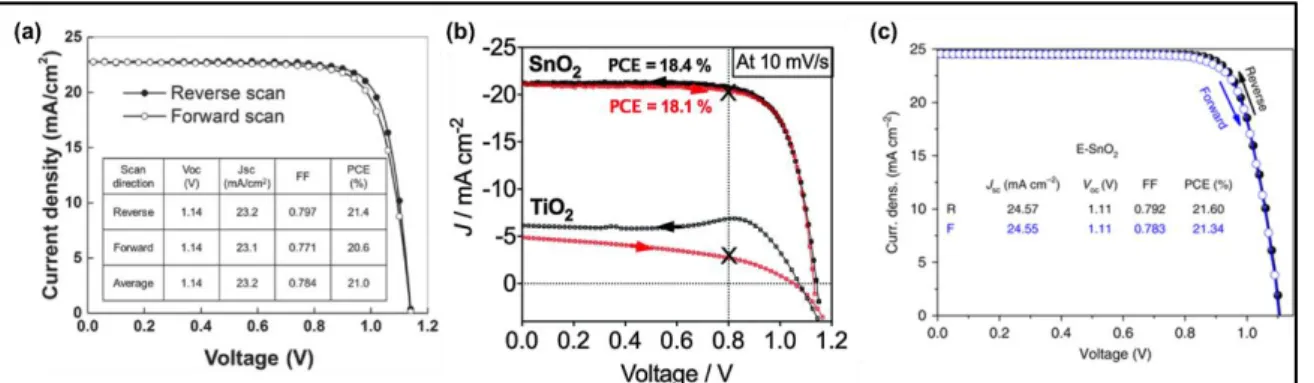
Besides improving the energy-level alignment of the conduction band minimum between β-CsPbI3 and TiO2 by 120 meV, CHI treatment fills the pinhole. The PSCs employing
CHI-treated material achieved a stable efficiency reaching 18.4% (certified PCE of 18.3%) recorded at 45 ± 5°C under ambient conditions. As shown in Figure 4d, although the Jsc remained unaffected, the CHI-CsPbI3-based PSC showed improved VOC (1.05 V to 1.11 V)
and FF (0.72 to 0.82).
Similar to CsPbI3, formamidinium lead iodide (FAPbI3) shows higher thermal stability
than MAPbI3. In addition, FAPbI3 exhibits a narrower bandgap (as compared to MAPbI3),
however, its structural instability remains a concern particularly in the presence of moisture. Reports show that such issues of yellow-phase formation (δ-FAPbI3, non-perovskite phase),
halide segregation, undesired phase transition, degradation under moisture can be eliminated by using perovskites with mixed-cations compositions. For the first time, Pellet et al.
introduced mixed-cation 3D perovskite, (MA)x(FA)1-xPbI3 (x = 0–1) as an absorber layer in
the mesoscopic PSCs.[60]The mixed-cation perovskite with MA
0.6FA0.4PbI3 composition
showed the best photovoltaic performance, which was attributed to the enhanced harvesting and collection of red photons. The longer exciton lifetime explained the superior carrier-collection efficiency of mixed-organic-cation perovskite. Wang et al. reported further
improvement in the device performance of (MA1−xFAxPbI3) by introducing a small amount of
lead thiocyanate (Pb(SCN)2) additive into mixed perovskite precursor solutions.[68] The
champion MA0.7FA0.3PbI3 PSCs with 3% Pb(SCN)2 additive showed PCE of 20.10% with a
VOC of 1.12 V. The increase in PCE was attributed to the enlarged grain size and prolonged
22
The dependence of VOC on the light intensity presented a lower slope for Pb(SCN)2
incorporated perovskite-based devices, revealing a lower Shockley–Read–Hall recombination (trap-assisted recombination) in the corresponding devices.
Recently, a new method was described for fabricating gradient heterostructure of PSCs based on “intolerant” trivalent metal cations such as Sb3+, and In3+.[69] In this study,
mixed-cation Cs0.1FA0.9PbI3 perovskite structure was employed as the active layer due to its
moderate Goldschmidt tolerant factor (τ = 0.9) and excellent photoelectrical
performance.[19,70] Both the Sb3+ and In3+ do not dissolve homogeneously in the perovskite solution due to large difference in ionic sizes and electrostatic interaction between the dopants and the host Pb atoms as shown in Figure 4e. Therefore, a graded heterojunction was formed spontaneously. As a result, Sb3+ doped PSCs reached a stabilized PCE of 21.04% with an extraordinary FF and VOC of 0.84 and 1.10 V, respectively. Both theoretical calculations and experimental observations specified optimized charge management as a result of the tailored band structure and interfacial electronic hybridization, promoting the charge separation and collection processes.
In order to tailor the band structure and electronic properties of perovskites, chemical modification realized by the substitution of I− with Br− as well as by the substitution of MA+
with different organic/inorganic cations have been applied as an efficient approach, resulting in colour variation, high stability, and PCE modulation. Compositional engineering of mixed-halide and mixed-cation perovskite materials has been first reported by combining the
unstable FAPbI3 with MAPbBr3 in (FAPbI3)1-x(MAPbBr3)x[71]. As shown in Figure 4f,
simultaneous introduction of 15 mol% of both MA+ cations and Br− anions in FAPbI
3 led to
the stabilization of (FAPbI3)0.85(MAPbBr3)0.15 perovskite phase. The trend in PCE as a
function of x showed that JSC increased from 19.0 mA cm−2 (at x = 0.05) to a maximum value of 22 mA cm−2 (at x = 0.15); and then decreased to 20 mA cm−2 (at x = 0.30), whereas VOC
23
increased from 1.0 V to 1.12 V with increasing x. The incorporation of MAPbBr3 not merely
stabilized FAPbI3 phase but also improved PCE more than 18% with negligible hysteresis.
Figure 4. a) EQE spectra and J–V curves of the annealed devices MAPbI3 (black),
MAPb(Br0.2I0.8)3 (red), and MAPb(Br0.5I0.5)3 (green) (solid lines show forward scans, while
dashed lines show reverse ones). Reproduced with permission.[65] Copyright 2018, American Chemical Society. b) Schematic illustration of crack-filling interface engineering and
corresponding energy diagrams of the CsPbI3 and choline iodine (CHI)-CsPbI3 films, CHI
treatment led to the improvement in the energy-level alignment of the conduction band minimum between β-CsPbI3 and TiO2. Reproduced with permission.[67] Copyright 2019,
American Association for the Advancement of Science. c) TRPL decay curves of CsPbI3 and
CHI-CsPbI3 thin films. Reproduced with permission.[67] Copyright 2019, American
Association for the Advancement of Science. d) J-V characteristics of the champion PSCs based on CsPbI3 and CHI-CsPbI3 with 0.1-cm2 effective cell area under simulated AM 1.5G
solar illumination of 100 mW cm−2 in reverse scan. Reproduced with permission.[67] Copyright 2019, American Association for the Advancement of Science. e)
RM – RPb/RPb (yellow solid circles) and tolerance factor (red solid circles) of
Cs0.1FA0.9MI3 perovskites, M = Pb2+, Sr2+, Bi3+, Sn2+, Cd2+, Mn2+, In3+, and Sb3+. Reproduced
with permission.[69] Copyright 2019, John Wiley & Sons. f) XRD patterns of solvent-engineering-processed FAPbI3, (FAPbI3)1 − x(MAPbI3)x, (FAPbI3)1 − x(FAPbBr3)x, and
(FAPbI3)1 − x(MAPbBr3)x perovskite films (with x = 0.15) on mesoporous-TiO2
/blocking-TiO2/FTO glass substrates. Reproduced with permission.[71] Copyright 2015, Nature
Publishing Group.
Lead thiocyanate (Pb(SCN)2) additive has also been used for the fabrication of
mixed-cation mixed-halide perovskite thin films. However, the formation of excessive lead iodide (PbI2) is still a big challenge limiting the utilization of the Pb(SCN)2 additive. Yu et al.
24
of solvent annealing and reported the synergistic effects on the performance of PSCs
employing wide-bandgap (bandgap of 1.75 eV) FA0.8Cs0.2Pb(I0.7Br0.3)3 light-absorber.[72] The
authors demonstrated that the cooperation of 1.0 mol % Pb(SCN)2 additive and solvent
annealing can successfully facilitate the formation of large grains while avoiding the
formation of excessive PbI2. As a result, the average PCE increased from 13.44 ± 0.48 % to
17.68 ± 0.36 % owing to the great improvement in the VOC (80 mV).
Among the various film modification approaches, polymer-assisted crystal
engineering has been found to be a robust method to increase the perovskite grain size. Bi et al. reported the poly(methyl methacrylate) (PMMA)-templated nucleation and crystal growth
of perovskite films.[73] The PMMA polymer played the dual role of enabling fast
heterogeneous nucleation and slowing down the perovskite crystal growth by forming an intermediate adduct with PbI2. As evidenced by the long PL lifetime, smooth and shiny
perovskite films with excellent electronic quality were obtained. By using the
(FAI)0.81(PbI2)0.85(MAPbBr3)0.15 perovskite absorber layer, a PCE of 21.6% (a certified PCE
of 21.02%) with VOC of 1.14 V, FF of 0.78, and JSC of 23.7 mA cm-2 was reported while the control devices showed a PCE of around 20% (Figure 5a).
In a similar direction bis-analogue of PCBM (bis-PCBM) was utilized as a templating agent in antisolvent to obtain high electronic quality perovskite films with low-defect
density.[74] It was reported that PCBM can fill the vacancies and grain boundaries on the
perovskite surface and thus improve the crystallization of final perovskite film. The
introduction of an electron-accepting PCBM into the (FAI)0.81(PbI2)0.85(MABr)0.15(PbBr2)0.15
film facilitated the slow electron extraction resulting in a PCE of 20.8%. The increase in JSC with PCBM was ascribed to the enhanced photoelectron transport, higher conductivity, and higher mobility whereas the origin of the improved VOC was the reduction of spontaneous trap-assisted non-radiative recombination.
25
Although MA-FA based perovskite materials dramatically improved the photovoltaic performance of PSCs, these compositions are sensitive to the processing conditions because of their intrinsic structural and thermal instability issues. To overcome these issues,
composition-additive engineering involving the mixing of MA/FA organic cations with small amounts of inorganic cations has been intensively investigated in recent years. High-quality perovskite films were obtained by incorporating a small amount of inorganic cesium (Cs) cation into the MA/FA composition. The obtained triple-cation
Cs0.05(MA0.17FA0.83)0.95Pb(I0.83Br0.17)3 perovskite absorber yielded a stabilized PCE exceeding
21% with a VOC of 1.13 V and excellent operational stability (Figure 5b).[21] In another study,
small and oxidation-stable rubidium cations (Rb+) were explored to further improve the properties of perovskite material and the photovoltaic efficiency of resulting PSCs.[22] Stabilized PCE of 21.6% with a VOC of 1.19 V was obtained from PSCs based on
RbCsMAFA perovskite composition containing 5% Rb additive. The best device showed an outstanding VOC of 1.24 V with a loss in the potential of only ~0.39 V, implying negligible nonradiative recombination losses. The obtained electroluminescence of 3.8% further
confirmed a strong suppression of nonradiative recombination in the RbCsMAFA device. The electrochemical characterization also brought out that the introduction of Rb+ improves the
interfacial charge transport characteristics in multiple-cation mixed-halide PSCs.[75,76]
Recently, in order to further boost the photovoltage of mixed-cation and mixed-halide based PSCs, guanidinium iodide (GuaI) was introduced into
Cs0.05(MA0.17FA0.83)0.95Pb(I0.83Br0.17)3 perovskite films.[77] GuaI led to the suppression of
parasitic charge-carrier recombination and enabled fabrication of efficient PSCs (>20% PCE) yielding reproducible VOC as high as 1.20 V (Figure 5c). The 70 mV enhancement in VOC was ascribed to the reduced non-radiative recombination as revealed by time-resolved
26
Figure 5. a) J-V curves of the champion PSC prepared by polymer-templated nucleation and
growth method displaying the best PCE of 21.6% with a PMMA concentration CPMMA =
0.6 mg ml−1. Reproduced with permission.[73] Copyright 2016, Nature Publishing Group. b)
J-V and stability characteristics (for the best performing Cs5M device. The inset shows the
power output under maximum power point tracking for 60 s. Reproduced with
permission.[21] Copyright 2016, Royal Society of Chemistry. c) J-V curves of the best devices based on Cs5Pb and Cs5Pb0.05GuaI perovskite films, 5% GuaI to Cs5Pb significantly
improved the VOC from 1.13 V to 1.20 V. Reproduced under the terms of the CC BY 4.0 license.[77] Copyright 2019, Science and Technology Review Publishing House (d) TRPL spectra of pure and GuaI containing perovskite films,charge carrier lifetime values of 215 ns and 627 ns were estimated, respectively, for the Cs5Pb, and Cs5Pb0.05GuaI perovskite films.
Reproduced under the terms of the CC BY 4.0 license.[77] Copyright 2019, Science and Technology Review Publishing House.
The suppression of defects resulting in an increase in the VOC has also been reported for halide-based additives. For example, Fu et al. introduced an additive-engineering strategy by adding formamidine acetate (FAAc) to the perovskite-precursor solution.[78] The role of FAAc was explained on the basis of chemical reactions between FAAc and methylammonium iodide (MAI) which forms formamidinium iodide (FAI) and methylammonium acetate
(MAAc). In this way, the number of I− vacancies could be reduced at the surface due to lower thermal stability of MAAc instead of MAI, leading to a reduced recombination rate in the resulting perovskite films. TRPL and thermogravimetric analysis (TGA) results confirmed the
27
stabilization of I− anions by Ac− anions. By using such an additive in
Cs0.05FA0.81MA0.14Pb(I2.55Br0.45) based perovskite film, the VOC of 1.19 V was achieved with
the best PCE of 21.9%.
3.2. ETL engineering in mixed cation and/or mixed halide perovskites
One of the most important layers in obtaining the high VOC is the ETL, which facilitates the extraction and transport of electron as discussed in section 2.2. Therefore, a suitable energy level alignment and a trap-free surface are critical to achieving admissible PCE. ETL
engineering is one of the most efficient ways to acquire a high-quality electron conductor with well-matched energy level and low trap-states and/or pin-holes. In this section, the remedial ETL engineering strategies employed for mixed-cation and/or mixed-halide based perovskite devices are discussed.
Zhou et al. reported the doping of TiO2 ETL with yttrium (Y3+) ions and modification
of ITO substrate with poly-ethyleneimine ethoxylated (PEIE) to suppress the carrier recombination in the perovskite film and to facilitate the carrier injection into the carrier transport layers[79]. By PEIE modification, the work function of ITO was reduced from -4.6
eV to -4.0 eV, whereas Y3+ doping increased the conduction band minimum (CBM) up to -4.0 eV. As a result of these modifications, a PCE (only reverse scan) of 19.3% with VOC of 1.15 V, was achieved for n-i-p-type PSCs in a planar configuration. The 110 mV increase in VOC was mainly attributed to the reduced non-ideal space charge distribution as a result of balanced carrier transport. Notably, the PCE measured by a reverse scan can be highly overestimated owing to the large-hysteresis index. The anomalous hysteresis in PSCs can mainly be explained by the evoking the charge migration or accumulation at the
perovskite/ETL interface. The enhancement in electrical properties and reduction in surface defects of ETL by suitable dopants can reduce the non-radiative recombination at the
28
perovskite/ETL interface and thereby properly alleviate the anomalous hysteresis behaviour of PSCs.
In an interesting study, a new mesoscopic architecture using Cs-doped TiO2 beads as
electron selective contact was described.[80] The enhancement of the contact area accessed by
the perovskite light absorber and interface passivation between perovskite and mp-TiO2 led to
the fabrication of efficient quadruple-cation (Rb/Cs/FA0.95MA0.05) perovskite-based PSCs
with negligible hysteresis (Figure 6a). This substantially reduced hysteresis as compared to the bare TiO2, which was attributed to less charge accumulation at the perovskite/Cs-doped
TiO2 interface. It was also demonstrated that Cs doping induces a shift of both oxygens (O) 1s
and titanium (Ti) 2p peaks to lower energy, thereby decreasing oxygen vacancy which functions as an electron trap. This study obviously showed that a reduction in recombination rate is directly related to the increase in VOC of devices. Another electron selective contact that has gained considerable attention for enhancement of photovoltage is SnO2, which has a
deeper conduction band and a suitable band alignment with the perovskite absorber. A low-temperature atomic layer deposition (ALD) method was reported to fabricate compact and pin-hole free SnO2 ETL for their application in planar PSCs exhibiting a high performance (>
18%) with high voltages up to 1.19 V.[81] The low hysteresis is a result of suitable band
alignment and good charge collection for SnO2 based devices, whereas, amorphous TiO2
based devices showed a strong hysteresis and a low JSC (Figure 6b). The UPS and femtosecond TA measurements indicated a barrier-free charge transport across the perovskite/SnO2 in contrast to the perovskite/TiO2 interface. Recently, the suppression of
hysteresis in planar-type PSCs was also reported using EDTA-complexed SnO2 ETL with a
striking PCE.[82] EDTA-complexed SnO2 provided a well-matched Fermi level with the
conduction band of mixed-cation FA0.95Cs0.05PbI3 perovskite structure, leading to a higher
29
times higher than that of the pristine SnO2. The record PCE of corresponding PSCs based on
EDTA-complexed SnO2 ETL was achieved to be 21.60% (certified as 21.52% by Newport)
while pristine SnO2 ETL based device showed only a PCE of 18.93%. As shown in (Figure 6c), the hysteresis in the EDTA-complexed SnO2 ETL based device drastically reduced because of the eliminated charge accumulation between perovskite and ETL interface. It was also reported that EDTA treatment made the SnO2 surface more hydrophilic, thus, decreasing
the Gibbs free energy for heterogeneous nucleation, resulting in high-quality perovskite films.
Figure 6. a) J-V curves of the top-performing devices prepared with CsBr‐doped mp‐TiO2 as
ETL. Reproduced with permission.[80] Copyright 2018, John Wiley & Sons. b) J-V properties of TiO2 and SnO2-based planar (FAPbI3)0.85(MAPbBr3)0.15 devices backward scan (black curve)
and reversed scan (red curve). Reproduced under the terms of the CC BY-NC 3.0 license.[81] Copyright 2015, Royal Society of Chemistry. c) J-V curves of the device using EDTA-complexed SnO2 E-SnO2 as ETL in forward and reverse direction. Reproduced under the
terms of the CC BY-NC 4.0 license.[82] Copyright 2018, Nature Publishing Group.
Gong et al. systematically investigated the band offset between ETL and
(FAPbI3)0.85(MAPbBr3)0.15 perovskite absorber by tuning F-doping level in gradient SnO2
based ETL.[83] A reduction in the band offset was reported by the gradual substitution of F− anions, resulting in a reduction in energy loss and a dramatic increase in VOC. By employing the bilayer ETLs, planar type PSCs reached to a PCE of 20.2% with a VOC of 1.13 V, while the control device showed a PCE of 16.3% with a VOC of 1.03 V. Compared to pristine SnO2
30
upward-shifted Fermi level. More importantly, in addition to longer lifetime constant of bilayer ETL/perovskite (∼356.5 ns) than that of pristine SnO2 ETL/perovskite (∼198.7 ns);
bilayer ETL exhibited better carrier collection and effectively suppressed the carrier recombination.
In a similar direction, a thin layer of LiF at the SnO2/perovskite interlayer was
introduced to fabricate high efficiency PSCs.[84] It was deduced that the LiF interlayer acts as
a highly efficient interfacial passivation layer between SnO2/perovskite interface without
influencing the surface topography and crystal quality of perovskite films as well as light absorption ability of devices. In the presence of 1 nm thick LiF layer, the VOC increased from 1.06 V to 1.16 V, indicating that LiF suppressed the interfacial trap states between
SnO2/perovskite and reduced the interfacial (parasitic) charge recombination. The role of Li+
and F− was also investigated separately, by using the interlayer of PbF2 (F− only) and LiTFSI
(Li+ only) layers. It was found that a thin PbF
2 modified SnO2 layer increased the VOC from
1.06 V to 1.14 V, while LiTFSI did not change it. Therefore, the effect of F− ions was the key factor in VOC improvement.
In addition to doping based modifications, the preparation of the ETL is also important to obtain efficient devices. A low-temperature solution-processed chemical bath deposition (CBD) method was described for Nb-doped SnO2 layers for almost hysteresis-free and highly
efficient (FAPbI3)0.85(MAPbBr3)0.15 perovskite-based planar type PSCs.[85] ETLs with an
optimum Nb-doping (5 mol.%) exhibited a lower series resistance, resulting in a higher FF (0.74 in average) and suppressed J-V hysteresis. This approach generated a VOC of 1.16 V and a significant PCE of 20.47% for the device employing 5 mol.% Nb-doped ETL. Such an improvement in VOC was attributed to the reduced recombination at the interface due to the formation of defect-free and high-quality surface coverage.
31
3.3. HTL engineering in mixed-cation and/or mixed-halide perovskites
As described in Section 2.3. HTLs play a key role in extracting and transporting the photo‐ generated holes and in achieving an admissible photovoltaic performance. In addition to reasonable hole mobility and high electrical conductivity, HTL should meet requirements such as well-aligned energy levels, low-cost synthesis, and excellent thermal/photochemical stability.[86,87] Towards this end, different strategies in HTL engineering, i.e. additives, molecular engineering, new materials, have been investigated. In the following section, some of the most representative reports regarding photovoltaic performance and stability of mixed-cation mixed-halide PSCs will be discussed.
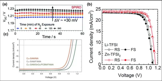
In spiro-OMeTAD based systems, the dopants play a key role in recombination
dynamics to limit the VOC because they act as recombination centres at the HTL interface. The effect of dopant concentration of spiro-OMeTAD was examined on the recombination
dynamics and it was found that the recombination is strongly dominated by the dopants and a VOC can significantly boost up to 1.23 V by reducing the Li-TFSI concentrations in
spiro-OMeTAD (Figure 7a).[88] However, lower dopant concentrations also yielded a lower FF,
resulting in a decrease in the overall PCE, showing that the dopant is indispensable in the case of spiro-OMeTAD owing to its low conductivity and hole mobility.
Other dopants have been also explored to enhance photovoltaic performance. Among the various alternates, Zn-TFSI2 was successfully employed in spiro-OMeTAD as a p-type dopant
by Seo et al., leading to improved hole mobility (from 3.78 х 10−3 cm2 V−1 s−1 to 3.83 х 10−2 cm2 V−1 s−1) and hole separation compared to the Li-TFSI.[89] The device with Zn-TFSI
2
exhibited an 80 mV higher built-in voltage and a larger recombination resistance as compared to those based on Li-TFSI, leading to the striking increase in both the VOC and FF. Zn-TFSI2
employing devices showed a stabilized PCE of 22% with a VOC of 1.15 V owing to the downward shifting of the Fermi level of spiro-OMeTAD (Figure 7b). Furthermore, Zn-TFSI2
32
employing devices presented an excellent photo-stability, showing even a 2% increase after 600 h light soaking. The remarkable photovoltaic performance was ascribed to the electronic properties of the Zn-TFSI2, whereas outstanding long-term stability was attributed to the static
nature and higher electric-field strength of the Zn ions, inducing a strong electrostatic interaction within the spiro-OMeTAD matrix.
Figure 7. a) VOC vs. time with nitrogen exposure for best-performing devices using spiro-OMeTAD as HTL. Reproduced with permission.[88] Copyright 2017, Royal Society of Chemistry. b) J-V curves of devices employing Li-TFSI or Zn-TFSI2 as a dopant for
spiro-OMeTAD. Reproduced with permission.[89] Copyright 2018, Royal Society of Chemistry. c) J-V curves of the maximized performance devices for MA perovskite using C60-SAM as ETL
(orange curve) and PDCBT/Ta-WOx as HTL, FAMA perovskite-based devices using C60
-SAM as ETL and PDCBT/Ta-WOx as HTL (gray curve), and FAMA perovskite-based devices using C60-SAM/SnOx/PC60BM as ETL and PDCBT/Ta-WOx as HTL (green curve).
Reproduced with permission.[91] Copyright 2017, American Association for the Advancement of Science.
In addition to TFSI based dopants, different additives have been also explored to reduce the non-radiative recombination losses. The synthesis and utilization of
adamantylammonium halides (ADAHX, X = Cl−, Br−, I−) as a promising dopant in spiro-OMeTAD was recently reported.[90] Solid-state NMR spectroscopy showed a strong
interaction between ADAHI and perovskite surface, resulting in highly efficient PSCs (22%). The insertion of ADAHI dopant into spiro-OMeTAD increased the VOC by 145 mV (from 1.10 V to 1.245 V). The loss in the potential for the corresponding devices was reported to be
33
only 365 mV with respect to the bandgap of 1.61 eV. The recombination behaviour at perovskite and HTL interface was investigated by electron beam-induced current (EBIC), which demonstrated a strong and uniform signal in the presence of ADAHI, indicating a lower recombination rate owing to the successful suppression of interfacial traps.
In addition to interfacial traps, the energy barriers between the HTL interfaces play a key role in minimizing the charge-carrier transport losses in PSCs. Bilayered HTLs are one of the best ways to decrease the energy barriers, which not only show a good selectivity but also a low-resistivity. Hou et al. reported tantalum-doped tungsten oxide (Ta-WOx) and a
polythiophene derivative, poly[5,5′-bis(2-butyloctyl)-(2,2′-bithiophene)-4,4′-dicarboxylate-alt-5,5′-2,2′-bithiophene] (PDCBT) conjugated polymer multilayers to reduce interfacial barrier and form quasi-ohmic contacts.[91] By employing the perovskite composition of FA0.83MA0.17Pb1.1Br0.50I2.80 and ionic dopant–free HTL, a PCE of 21.2% with negligible
hysteresis was achieved (Figure 7c). A thin coating of high conductive Ta-WOx film onto
PDCBT showed a shift of 0.5 eV in work function, implying much more effective charge transfer from the polymer to the metal oxides.
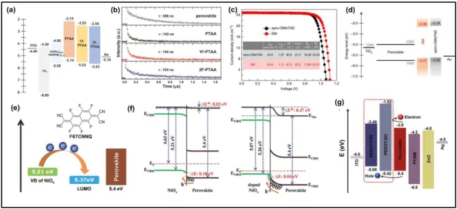
The concept of molecular engineering of the perovskite layer and HTL is crucial to increase the VOC and improve the performance of PSCs. In general, a higher Voc is obtained for HTMs with a higher oxidation potential. However, factors like intrinsic mobility of the HTM material, optimization of HTM molecular structure are equally important to enhance VOC. The introduction of an electron-withdrawing group such as fluorine with a high
electronegativity to organic conjugated materials has been demonstrated as an efficient route to alleviate the charge transfer by controlling the energetic offset and improve the VOC values of polymer-based PSCs. For example, Kim et al. investigated the impact of fluorination on poly(triarylamine) (PTAA) polymers hole-transporting materials in
34
successfully led to downshifting of the highest occupied molecular orbital (HOMO) level of PTAA derivatives (−5.14 eV to −5.63 eV), leading to an increase in the VOC (1.10 V to 1.14 V) (Figure 8a and 8b). Space-charge-limited current (SCLC) measurements revealed hole mobility in the order of 10−5 while TRPL measurement showed a better charge extraction from perovskite compared with the reference PTAA HTL.
In a similar direction, fluorene-terminated HTL material ((N2,N2′,N7,N7′-tetrakis(9,9- dimethyl-9H-fluoren-2-yl)-N2,N2′,N7,N7′-tetrakis(4-methoxyphenyl)-,9′-spirobi[fluorene]-2,2′,7,7′-tetraamine)) (abbreviated as DM) with a high glass transition temperature was synthesized for efficient (FAPbI3)0.95(MAPbBr3)0.05 based PSCs. By using obtained material,
PCE of 22.9% with certified efficiencies of 22.6% for small-area (~0.094 cm2) devices and 20.9% for large-area (~1 cm2) was demonstrated (Figure 8c).[93] The obtained VOC of 1.14 V was ascribed to the slightly higher oxidation potential of DM HTL, leading to better energy-level matching with the perovskite as shown in (Figure 8d). HTL engineering strategies have also been applied for inverted device architecture in order to further improve the photovoltaic performance stability. In the inverted structure of PSCs, nickel oxide (NiO) is one of the most efficient HTL material owing to its wide bandgap, high hole mobility, and appropriate valence band edge.[94,95] Bai et al. demonstrated that surface modification of NiO HTL in inverted
type PSC with di-ethanolamine (DEA) molecules can enhance the hole extraction/transport and thus the photovoltaic performance.[96] The enhancement in photovoltaic performance was
ascribed to the favourable layer formed by the molecular adsorption and the better interfacial interaction. The molecular adsorption creates a dipole layer, which is favourably oriented for hole extraction resulting in higher device performance (FF: 0.80 and PCE: 15.9%) for DEA based PSC than the control device (FF: 0.65 and PCE: 11.2%).
Recently, molecular doping was introduced to modify the solution-derived NiOx HTLs
2,2′-(perfluoronaphthalene-2,6-35
diylidene)dimalononitrile (F6TCNNQ) onto the bare NiOx.[97] This approach helped the
molecular dopants to penetrate into the grain boundaries of the bare NiOx film, which resulted
in a strong p-type doping effect, thus leading to a remarkable reduction in contact resistance at the NiOx–perovskite interface. Moreover, the Fermi level of NiOx was increased from 4.63 eV
to 5.07 eV after the F6TCNNQ doping, while the valence band maximum (VBM) level was decreased from 5.21 eV to 5.37 eV, leading to an increase in VOC and overall PCE in inverted CsFAMAPb(IBr)3-based devices, owing to the minimized thermionic losses (Figure 8e and f).
Very recently, low temperature and solution-combustion based method was employed to prepare the NiOx HTL.[98] The resulting NiOx exhibited a high film quality, slightly larger
bandgap and preferable energy alignment with respect to MA1−yFAyPbI3−xClx perovskite layer
compared to high-temperature sol-gel‐processed NiOx. The devices employing combustion-derived NiOx showed that the perovskite films on corresponding HTL had larger grain size with fewer defect states, exhibiting a high PCE of 20.2% with a remarkable VOC of 1.12 V. The improved PCE and enhanced ambient air storage stability was ascribed to the high quality of perovskite/HTL interface resulting in an enhanced charge transport, extraction, and suppressed charge recombination whereas the enhancement in VOC was attributed to the decreased work function which increases the potential difference between valance band of NiOx and conduction band of perovskite.
In addition to inorganic NiO HTL, organic-based poly(3,4-ethylenedioxythiophene): poly(styrene sulfonate) (PEDOT: PSS) is widely used as an HTL material in perovskite devices owing to its low-temperature processability, suitable valance band maximum, and low surface roughness. However, the high acidic nature and large energy barrier between the perovskite/PEDOT: PSS layers limit the hole extraction. To improve the hole extraction properties of PEDOT: PSS HTL, several attempts have been reported. For example, graphene