the Wilkinson Divider
Vahdettin Tas, Student Member, IEEE, and Abdullah Atalar, Fellow, IEEE
Abstract—We propose an isolation network to simultaneouslyimprove the input return loss, output return loss and isolation of the Wilkinson power divider in a wide bandwidth. The required even mode and odd mode reflection coefficients of the isolation net-work are calculated. Constructed even and odd mode circuits are combined to give the desired isolation network. Analytical expres-sions for the optimal component values for a single-section divider are given. Compared with the single-section Wilkinson divider, the final design can triple the bandwidth for an input-output return loss and isolation of greater than 25 dB. Broadband characteristic is achieved without increasing the number of sections hence extra length and insertion loss are avoided. Wide operation bandwidth of the new divider is verified by experimental results. The proposed method can be applied to a two-section divider, also broadening its bandwidth.
Index Terms—Even mode, isolation network, odd mode, reflec-tion coefficients, wideband power divider, Wilkinson divider.
I. INTRODUCTION
P
OWER dividers are used at microwave frequencies to di-rect the power to two or more loads. Normally, they main-tain the matched condition at all ports within the operation band. Moreover, a good isolation between the output ports is desired to eliminate the interaction between the loads. When used in the opposite direction, power dividers can combine power from two or more power sources. The Wilkinson power divider was in-troduced in 1960 [1]. Around the center frequency it is matched at all ports and isolated at the output ports within a relatively narrow bandwidth. Cohn [2] introduced the multisection hy-brids to improve the operation bandwidth of the Wilkinson di-vider. Broadband power division using multisection structures was revealed in several studies [3]–[8]. Wide operation band-width is also achieved by utilizing tapered lines. They are con-structed using a continuum of a long tapered line [9] or multi-section tapered lines [10]. The main disadvantage of using multi sections is the increase in the length and the insertion loss of the divider. To avoid this, a number of researchers designed re-duced size dividers [11]–[14]. Another approach to improve the bandwidth response of the Wilkinson divider aims dual band Manuscript received June 30, 2014; revised September 22, 2014; accepted October 23, 2014. Date of publication November 14, 2014; date of current ver-sion December 02, 2014. This paper is an expanded verver-sion from the IEEE MTT-S International Microwave Symposium, Tampa Bay, FL, USA, June 1-6 2014.The authors are with the Department of Electrical and Electronics Engi-neering, Bilkent University, Ankara 06800, Turkey (e-mail: [email protected]. edu.tr; [email protected]).
Color versions of one or more of the figures in this paper are available online at http://ieeexplore.ieee.org.
Digital Object Identifier 10.1109/TMTT.2014.2365533
operation. This is achieved by using networks in series or parallel configuration between the output ports [15]–[17], cou-pled lines [18], parallel stubs along the transmission path [19] and right-left handed transmission lines [20]. These designs also require an increase in length. Other works [21], [22] focus on the isolation network design for isolation bandwidth improve-ment. Length increment is avoided by modifying only the isola-tion network. In these works, the isolaisola-tion bandwidth is widened while the input return loss is kept unchanged. Due to the posi-tion of the isolaposi-tion resistors extra inserposi-tion loss is faced.
Our goal is to design an isolation network that improves the bandwidth of input return loss, output return loss and isola-tion, simultaneously. This way, the number of sections is not increased hence extra length and loss are avoided. We first de-rive an equation relating the input return loss, output return loss and isolation values of a symmetrical two way power divider. Then we calculate the optimal reflection coefficients of the iso-lation network in the even mode and odd mode cases. Circuits are constructed to realize the calculated reflection coefficients. The resulting circuits are combined in the final divider structure. Preliminary experimental results of the single-section divider were presented in [23]. Here, detailed analytical work and sim-ulation results for the single and two-section dividers are pre-sented along with new experimental results.
II. S-PARAMETERRELATION FOR A LOSSLESS SYMMETRICAL2-WAYDIVIDER
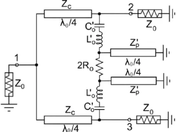
In Fig. 1, a symmetrical multisection 2-way combiner/di-vider network is depicted. The network is composed of lossless lumped or distributed components apart from the isolation arms shown with gray boxes. The contents of the gray boxes are delineated in Fig. 2. It is composed of symmetrical white boxes with resistors in the middle. The white boxes in Figs. 1 and 2 can have more than one series or shunt lossless components as long as the symmetry between the arms is maintained. S-parameter matrix equation of such a three port is given by
(1) where and are the incident and reflected powers at port . can be expressed as
(2)
If and are applied, we find
(3) 0018-9480 © 2014 IEEE. Personal use is permitted, but republication/redistribution requires IEEE permission.
Fig. 2. Possible contents of a gray box: Symmetrical lossless white boxes with isolation resistors in the middle.
(4) The incident power is . Due to the even exci-tation, there is no dissipation in the isolation arms, and the total incident power equals the transmitted power plus the total re-flected power:
(5) From (3)–(5) we find
(6) and finally we arrive at the result1
(7) Corollary 1: For the generic 2-way divider of Fig. 1, if
and , then , and
.
Proof: Defining and
, where and are arbitrary angles, we have
(8) (9) directly follows from (7).
For the generalized two-way divider in Fig. 1, the excitation , , results in the even mode operation. The S-parameter matrix (1) can be rewritten as
(10)
1Equation (7) was implicitly stated in [2].
Fig. 3. (a) Single-section Wilkinson divider with a gray box in the isolation arm. (b) Even mode equivalent circuit. c) Odd mode equivalent circuit. So, the reflection coefficient at the second port equals to
(11)
Similarly, the excitation , , results
in the odd mode operation. The S-parameter matrix (1) can be rewritten as
(12) So, the reflection coefficient at the second port equals to
(13)
and are the even mode and odd
mode reflection coefficients at port 2. From Corollary 1 we can conclude that keeping the even mode and odd mode reflection coefficients at port 2 below a certain level assures that the input-output return loss and isolation parameters are kept below the same level.
In the literature, broadband operation of the power dividers is generally achieved at the expense of an increase in the length and insertion loss of the dividers. In those designs, the isola-tion networks are composed of floating components without a ground connection, hence the isolation network does not affect the even mode circuit. Consequently, the input return loss can not be tuned by the isolation network. This is a significant loss of a degree of freedom. By the inclusion of components with a ground connection, the isolation network can be active both in the even mode as well as in the odd mode. With such an ap-proach both and can be tuned by the iso-lation network.
III. OPTIMALCHOICE OF ISOLATIONNETWORK IN THEEVEN ANDODDMODES
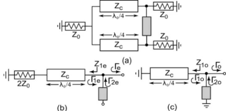
Our goal is to find an optimal isolation network for the single-section Wilkinson divider depicted in Fig. 3(a). The isolation network is represented with a gray box. can be different than for generality. Fig. 3(b) and (c) shows the even and odd mode equivalent circuits with the gray box open-circuited and shorted at its mid point, respectively.
Fig. 4. Two networks connected in parallel. One has an input impedance of , the other one has an input reflection coefficient of to give . For a parallel connection of two one-port networks shown in Fig. 4, the perfect match condition requires
(14) where is the normalized input impedance of the first block and is the input reflection coefficient of the second block giving the perfect match.
The normalized impedances and defined in Fig. 3 are equal to
(15) (16)
where is the center frequency and .
The reflection coefficients and of the even and odd mode isolation circuits that will generate a perfect match can be calculated using (14), (15), and (16):
(17) (18)
A. Even Mode Isolation Circuit
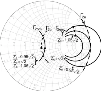
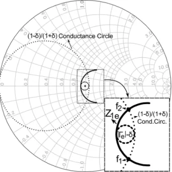
The trajectory of is drawn on the Smith chart of Fig. 5
for , and . Even mode isolation
cir-cuit must be lossless, otherwise the insertion loss of the divider will increase. So, its reflection coefficient must lie on the unity circle of the Smith chart. characteristic can be approxi-mated with a shorted quarter-wave stub of impedance as in Fig. 6. The corresponding is depicted by dashed lines in Fig. 5. For , and coincide only at the center frequency and deviate fast with frequency. For , the situation is even worse. With , , and coincide at two frequencies and the highest deviation occurs at the center frequency, , and at band edges. This characteristic resembles a second degree Chebyshev response maximizing the bandwidth. So, we choose to have a wideband approximation. The deviation at can be adjusted by the value of . At , the shorted quarter-wave stub acts like an open-circuit. Using Corollary-1 we aim to satisfy . The deviation is
max-Fig. 5. and on the Smith chart (solid lines) as the frequency is swept from to (in the direction of arrows) for , and . Approximations, and , (dashed lines) are also shown.
Fig. 6. Even mode equivalent circuit with the shorted quarter-wave stub of impedance at the isolation arm.
imum at , so . Referring to Fig. 6, since at , the value of is equal to
(19) Hence, we have
(20) To calculate the bandwidth and the optimal value of , we refer to the Smith chart shown in Fig. 7. The goal is to bend the trajectory into the circle using the shorted transmission line with the characteristic impedance of . The lowest normalized conductance on the locus of the
circle is . So, the frequencies at which re-sults a conductance of are the minimum and the maximum frequencies satisfying the condition. The lower and upper frequencies are marked as and , respec-tively, in Fig. 7.
At , we have:
(21) Using (15) and (20), (21) can be expanded as
Fig. 7. Trajectories of the constant conductance circle and circle along with the trajectory of (shown in Fig. 6).
We find
(23) For small , we can ignore the term, and write as
(24)
We note that . For example, for
dB , and .
The value of is calculated by considering that the imagi-nary part of the admittance should be compensated per-fectly at :
(25) So, we have
(26) Using (24) the value of is extracted from (26) as
(27) approaches to as gets closer to zero. With , (27) results in
If a lumped circuit is preferred, this shorted line can be approximated as a parallel circuit [24] with the component values expressed as
(28)
Fig. 8. Odd mode equivalent circuit with the optimal isolation network. and are resonant at the center frequency .
Fig. 9. Trajectories of the constant conductance circle and circle along with the trajectory of of Fig. 8.
B. Odd Mode Isolation Circuit
Smith chart trajectories of for three different values (which are almost equal to each other) are shown in Fig. 5. The locus of follows a constant conductance circle. A series circuit resonant at shown in Fig. 8 can be utilized to approximate the desired characteristics.
The same approach as the even mode case is followed to cal-culate the component values of the odd mode isolation network analytically. Referring to Fig. 8, is the reflection coefficient of the series network. The goal is to maximize the bandwidth of the condition. Fig. 9 shows the circle on the Smith chart together with the trajectory of . The points marked as and represent the edge frequencies that can be fitted into the circle by the shorted stub of impedance .
The impedance of a series resonator is not symmetric
around the center frequency. We have .
Therefore, is the bandwidth of the
con-dition. For the circuit in Fig. 8 at , resonates with and the quarter-wave stub is open-circuit. We have
. As shown in Fig. 9, . So, the value of the resistor is equal to
Fig. 10. Schematic diagram of the divider by merging the optimal even mode and odd mode isolation networks.
can be calculated by imposing two conditions at . trajectory crosses the conductance circle and the transmission line with the impedance of compensates the reactive part of perfectly. So, we have two equations:
(30)
(31) Using (29) and (30) we find
(32) Inserting (32) in the denominator of (31) and using (20), is calculated as
(33) Equation (33) together with (32) result in
(34)
For example, with and , we find
and . We note that the odd mode band-width is greater than the even mode bandband-width.
IV. COMBINING THE EVEN AND ODD MODE ISOLATIONNETWORKS
We merge the isolation circuits of Figs. 6 and 8 as shown in Fig. 10. Fig. 11 depicts the approximations involved in the merging process. Due to the interaction between the even and odd mode networks, some component values are shown with a prime symbol to indicate a possible modification in the calcu-lated component values of the previous section.
The value of was determined in the even mode circuit by the condition at . Since the isolation network does not affect
Fig. 11. Equivalent representation of the isolation network for the divider in Fig. 10. (a) Odd-mode. (b) Even-mode.
Fig. 12. Even (upper) and odd (lower) mode equivalent circuits of the divider in Fig. 10.
the even mode circuit at , value of (20) will not be mod-ified. Similarly, was determined in the odd mode circuit by the condition at . Since is open circuit at , the value of
given in (29) will not change.
The new values of and can be calculated following the analysis of the previous sections. Fig. 12 shows the even and odd mode equivalent circuits of the divider. Referring to Fig. 12(a), (26) is modified due to the presence of and :
(35) where is expressed in (24). is independent of the problem handled here, it is determined solely by .
From Fig. 12(b), (30) and (31) are modified to
(36)
(37) is used instead of the in (33) because it is dependent on and . A simultaneous solution of (35), (36), and (37) to find
Fig. 13. Normalized bandwidth comparison of the prosed divider structure with the classical single-section Wilkinson divider and Cohn’s design of two-section Wilkinson divider [2].
error in these equations are minimized numerically. Results of the numerical calculations are used to express and by the following approximations
(38) (39) Table I lists the results normalized with . The achievable normalized bandwidth and required component values for the corresponding level are listed. The divider bandwidth, , is limited by the bandwidth of the even mode circuit:
. , , , , and are determined from (20), (24), (29), (38), and (39), respectively. is resonant with at . Our results are verified using a microwave circuit simulator.2 It is possible to apply the proposed method to a two-section divider. Using a similar isolation arm for both sections, it is possible to extend the bandwidth considerably. The results for the two-section case are given in Appendix A.
Fig. 13 compares the bandwidth capabilities of the proposed section and two-section dividers with the classical single-section Wilkinson divider and Cohn’s two-single-section Wilkinson divider [2]. A significant bandwidth improvement is achieved. For 25 dB of input–output return loss and isolation, three times wider bandwidth is obtained in comparison to a single-section Wilkinson. The bandwidth of a two-section Wilkinson divider
2AWR Corp. El Segundo, CA 90245, USA, http://www.awrcorp.com
Fig. 14. Implemented 2-way power divider of Fig. 10.
is almost reached with a single-section divider, avoiding the extra size and insertion loss of the two-section divider.
In terms of insertion loss, the proposed divider is similar to a single-section Wilkinson divider, because the input signal prop-agates a distance of exactly one quarter wavelength. In fact, our divider is more advantageous in terms of the loss, since the impedance transforming line has a characteristic impedance smaller than resulting in a wider line width. Considering the size of the divider, the line in the isolation arm is shorted at one end and it has a high characteristic impedance with a narrow width. This enables one to use layout techniques such as bending or meandering of the line to get a compact size. We note that a two-section Wilkinson divider with two isola-tion resistors cannot be shaped in the same manner to reduce the size.
We note that presence of a ground path in the isolation net-work generates nulls in . These frequencies can be calcu-lated by considering the sum of the impedances of the line
and pair:
(40) Using (38) and (39), (40) can be rewritten as
(41) For example, for dB , (41) is satisfied at two fre-quencies, at and , outside the operation bandwidth
of the divider.
V. SIMULATION ANDEXPERIMENTALRESULTS The proposed divider in Fig. 10 is implemented for experi-mental verification at a center frequency of GHz.
Fig. 15. Simulated S-parameter characteristics of the divider in Fig. 14.
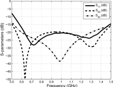
Fig. 16. Measured S-parameter characteristics of the divider in Fig. 14.
Fig. 17. Simulated (upper) and measured (lower) S-parameter characteristics of the divider in Fig. 14.
dB is the design goal. As shown in Table I, the theoretical fractional bandwidth is implying a 20-dB band-width of 0.6 GHz to 1.4 GHz. The divider is simulated using
Fig. 18. Modified version of divider in Fig. 14 upon the replacement of the shorted lines with the parallel resonators.
Fig. 19. Simulated response of the divider in Fig. 18.
the microwave circuit simulator and an electromagnetic simu-lator.3With ideal components, is achieved using the values given in Table I. Inclusion of the junction effects and component parasitics result in a reduction of the bandwidth. To alleviate these effects, the component values are tuned slightly. Fig. 14 shows the photo of the divider implemented on a RO40034substrate with a thickness of 0.8 mm. inductors are implemented using high impedance microstrip lines of 0.3 mm in width and 6.7 mm in length. Presence of in the isola-tion circuit provides a natural separaisola-tion between ports 2 and 3, reducing the length of subsequent connections and improving the isolation between the output ports [25], [26]. In the divider of Fig. 14, the width of lines are 1.1 mm corresponding to a characteristic impedance of . lines have a width of 0.3 mm resulting in an impedance of . 0603 package 5.6-pF capacitors and a resistor are used. Figs. 15 and 17 show the simulation results of the electromagnetic simulator. The output return loss and the isolation are better than 20 dB in the targeted
3SONNET Software, North Syracuse NY 13212, USA,
http://www.sonnet-software.com
Fig. 20. Measured response of the divider in Fig. 18. TABLE II COMPARISONTABLE
bandwidth, the input return loss drops to 17 dB at the band edges due to the nonideal effects.
Measured input–output return loss, isolation and insertion loss responses are shown in Figs. 16 and 17. The measurement results match the simulation results well. In the operation band, the extra insertion loss is less than 0.2 dB and the amplitude mismatch between the output ports is lower than 0.025 dB.
As discussed in (28) of Section III-A, the shorted lines at the isolation arm can be replaced with lumped components. For a verification, a modified version of the divider in Fig. 14 is im-plemented (Fig. 18). Equation (28) results in nH and pF for characteristic impedance and 1-GHz center frequency. Available chip inductor with a value closest
Fig. 21. Two-section divider with the optimal isolation networks.
Fig. 22. Even mode (a) and odd mode (b) equivalent circuits of the divider in Fig. 21.
TABLE III
NORMALIZEDCOMPONENTVALUES FORINPUT–OUTPUTRETURNLOSSES AND
ISOLATIONBETTERTHAN (dB)FOR THEDIVIDER INFIG. 21
to the calculated one is a 20-nH 0805 package chip inductor. S-parameter data provided by the manufacturer shows that the equivalent inductance of the 20-nH chip inductor increases up to 35 nH at 2 GHz due to the parasitic capacitance. This requires a reduction in the calculated value of . The best performance is obtained using a 0.8-pF capacitor. Figs. 19 and 20 show the sim-ulated and measured results, respectively. The characteristic is similar to the case with the shorted line. 19-dB bandwidth spans the 0.6 GHz to 1.35 GHz frequency range. The insertion loss is again below 0.2 dB in the operation bandwidth.
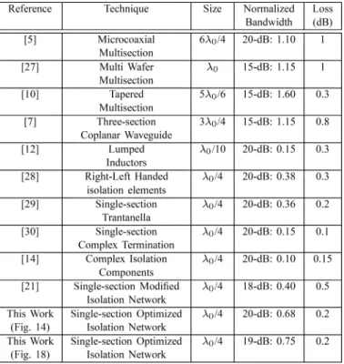
Table II is a comparison5of the dividers of recent studies. Given normalized bandwidth values are valid at the specified
5The loss comparison in the table is not totally fair, because the upper
fre-quencies and the substrate materials of the dividers listed in the table are not the same.
ponents. This increases the circuit implementation complexity and the parasitic problem.
VI. CONCLUSION
Starting from a fundamental S-parameter relation of a lossless power divider, we find that minimizing the even and odd mode reflection coefficients of an output port is sufficient to optimize a power divider. Using this fact, we are able to synthesize even and odd mode isolation networks to maximize the bandwidth of a single-section Wilkinson divider. The reflection coefficients of the isolation network that perfectly match the even and odd mode circuits are calculated individually. Then, circuits are de-signed to realize the required reflection coefficients. The even mode and odd mode isolation networks are merged in a config-uration to load each other minimally. Analytical expressions are derived for the component values of those networks. A modifi-cation in the final component values may be required to alleviate the loading effects. Table I lists the optimal component values. The resulting divider has a considerably wider operation bandwidth compared to the classical Wilkinson divider. Ex-perimental verification is presented proving that the proposed low-loss divider is promising for wide band applications. The method can be applied to a two-section divider. Using a similar isolation arm for both sections, it is possible to extend the bandwidth considerably.
APPENDIX
TWO-SECTION DIVIDERWITH THEOPTIMIZED ISOLATIONNETWORKS
The optimized isolation network is applied to the two-section case as shown in Fig. 21. The even mode and odd mode equiv-alent circuits are shown in Fig. 22. and represent the input impedances in each mode, respectively.
At , the even mode circuit shown in Fig. 22(a) is composed of only and . They provide an impedance transforma-tion from to . The optimal impedance values satisfy the geometric mean condition [31]:
(42) By allowing a nonzero reflection coefficient magnitude of , the bandwidth of operation can be extended. At the band center, , we have a real reflection coefficient of [23]. So, we can write
(43) Using (42) and (43), and are calculated as
(44) (45)
(46) where
(47) The odd mode input impedance can be expressed as
(48) where
(49) The optimal values of the remaining components are found by solving (46) and (48) numerically for the maximal bandwidth. The results indicate that the pair is not needed. For 20 dB and 25 dB cases pair is also absent and hence the first iso-lation network consists of only a resistor, . The normalized component values verified using a microwave circuit simulator are tabulated in Table III. The performance of this divider is de-picted in Fig. 13. Its bandwidth is considerably better than that of a two-section Wilkinson divider.
REFERENCES
[1] E. Wilkinson, “An N-way hybrid power divider,” IEEE Trans. Microw.
Theory Tech., vol. MTT-8, no. 1, pp. 116–118, Jan. 1960.
[2] S. Cohn, “A class of broadband three-port TEM-mode hybrids,” IEEE
Trans. Microw. Theory Tech., vol. MTT-19, no. 2, pp. 110–116, Feb.
1968.
[3] R. Ekinge, “A new method of synthesizing matched broad-band TEM-mode three-ports,” IEEE Trans. Microw. Theory Tech., vol. MTT-19, no. 1, pp. 81–88, Jan. 1971.
[4] H. Oraizi and A.-R. Sharifi, “Design and optimization of broadband asymmetrical multisection Wilkinson power divider,” IEEE Trans.
Mi-crow. Theory Tech., vol. 54, no. 5, pp. 2220–2231, May 2006.
[5] N. Ehsan, K. Vanhille, S. Rondineau, E. Cullens, and Z. Popovic, “Broadband micro-coaxial Wilkinson dividers,” IEEE Trans. Microw.
Theory Tech., vol. 57, no. 11, pp. 2783–2789, Nov. 2009.
[6] J.-C. Chieh and A.-V. Pham, “Development of a broadband Wilkinson power combiner on liquid crystal polymer,” in Proc. Asia Pacific
G-MTT Int. Microwave Symp., May 1968, pp. 16–20.
[10] C. T. Chiang and B.-K. Chaung, “Ultra wideband power divider using tapered line,” Progress In Electromagnetics Res, vol. 106, pp. 61–73, 2010.
[11] K. Hettak, G. Morin, and M. Stubbs, “Compact mmic cpw and asym-metric cps branch-line couplers and Wilkinson dividers using shunt and series stub loading,” IEEE Trans. Microw. Theory Tech., vol. 53, no. 5, pp. 1624–1635, May 2005.
[12] R. Mirzavand, M. Honari, A. Abdipour, and G. Moradi, “Compact mi-crostrip Wilkinson power dividers with harmonic suppression and ar-bitrary power division ratios,” IEEE Trans. Microw. Theory Tech., vol. 61, no. 1, pp. 61–68, Jan. 2013.
[13] Y.-S. Lin and J.-H. Lee, “Miniature ultra-wideband power divider using bridged t-coils,” IEEE Microw. Compon. Lett., vol. 22, no. 8, pp. 391–393, Aug. 2012.
[14] X. Wang, I. Sakagami, A. Mase, and M. Ichimura, “Wilkinson power divider with complex isolation component and its miniaturization,”
IEEE Trans. Microw. Theory Tech., vol. 62, no. 3, pp. 422–430, Mar.
2014.
[15] T. Kawai, J. Yamasaki, Y. Kokubo, and I. Ohta, “A design method of dual-frequency Wilkinson power divider,” in Proc. Asia Pacific
Mi-crow. Conf., 2006, pp. 913–916.
[16] X. Wang and I. Sakagami, “Generalized dual-frequency Wilkinson power dividers with a series/parallel RLC circuit,” in Proc. IEEE
MTT-S Int. Microw. Symp. Dig., Jun. 2011, pp. 1–4.
[17] Y. Wu, Y. Liu, and S. Li, “Unequal dual-frequency Wilkinson power divider including series resistor-inductor-capacitor isolation structure,”
IET Microw. Antennas Propag., vol. 3, no. 7, pp. 1079–1085, 2009.
[18] Y. Wu, Y. Liu, and Q. Xue, “An analytical approach for a novel cou-pled-line dual-band Wilkinson power divider,” IEEE Trans. Microw.
Theory Tech., vol. 59, no. 2, pp. 286–294, Feb. 2011.
[19] Y. Wu, Y. Liu, Y. Zhang, J. Gao, and H. Zhou, “A dual band unequal Wilkinson power divider without reactive components,” IEEE Trans.
Microw. Theory Tech., vol. 57, no. 1, pp. 216–222, Jan. 2009.
[20] A. Genc and R. Baktur, “Dual-and triple-band Wilkinson power dividers based on composite right-and left-handed transmission lines,”
IEEE Trans. Compon. Packag. Manuf. Technol., vol. 1, no. 3, pp.
327–334, Mar. 2011.
[21] J.-C. Kao, Z.-M. Tsai, K.-Y. Lin, and H. Wang, “A modified Wilkinson power divider with isolation bandwidth improvement,” IEEE Trans.
Microw. Theory Tech., vol. 60, no. 9, pp. 2768–2780, Sep. 2012.
[22] S.-F. Chao and Y.-R Li, “Miniature filtering power divider with increased isolation bandwidth,” Electron. Lett., vol. 50, no. 8, pp. 608–610, Apr. 2014.
[23] V. Tas and A. Atalar, “A performance enhanced power divider struc-ture,” in IEEE MTT-S Int. Microw. Symp. Dig., 2014, pp. 1–4. [24] D. M. Pozar, Microwave Engineering. New York, NY, USA: Wiley,
1998.
[25] S. Horst, R. Bairavasubramanian, M. Tentzeris, and J. Papapolymerou, “Modified Wilkinson power dividers for millimeter-wave integrated circuits,” IEEE Trans. Microw. Theory Tech., vol. 55, no. 11, pp. 2439–2446, Nov. 2007.
Wilkinson divider using zero-degree phase shifting composite right/left-handed transmission line,” in IEEE MTT-S Int. Microw.
Symp. Dig., 2010, pp. 1556–1559.
[29] X. wang, I. Sakagami, A. Mase, and M. Ichimura, “Trantanella Wilkinson power divider with additional transmission lines for simple layout,” IET Microw. Antennas Propag., vol. 8, no. 9, pp. 666–672, Jun. 2014.
[30] H. R. Ahn and S. Nam, “3-dB power dividers with equal complex termination impedances and design methods for controlling isolation circuits,” IEEE Trans. Microw. Theory Tech., vol. 61, no. 11, pp. 3872–3883, Nov. 2013.
[31] S. B. Cohn, “Optimum design of stepped transmission-line trans-formers,” IRE Trans. Microw. Theory Tech., vol. MTT-3, no. 3, pp. 16–20, Apr. 1955.
Vahdettin Tas (S’14) received the B.S. degree from
Middle East Technical University, Ankara, Turkey, in 2007 and the M.S. degree from Bilkent Univer-sity, Ankara, Turkey, in 2009, both in electrical en-gineering, where he is currently pursuing the Ph.D. degree.
In 2009, he was with the Electrical Engineering and Computer Science Department, University of California, Berkeley, CA, USA, as a Research Assistant. From 2010 to 2011, he was an RF Design Engineer at Meteksan Defense, Inc. Since 2011, he has been with the Power Amplifier Technologies Divison, Aselsan, Inc. His current research interests include broadband and efficient power amplification, power coupling, and power combining techniques.
Abdullah Atalar (M’88–SM’90–F’07) received the
B.S. degree from Middle East Technical University, Ankara, Turkey, in 1974, and the M.S. and Ph.D. de-grees from Stanford University, Stanford, CA, USA, in 1976 and 1978, respectively, all in electrical engi-neering.
He was with Hewlett Packard Labs, Palo Alto, CA, USA, in 1979. From 1980 to 1986, he was on the fac-ulty of the Middle East Technical University as an Assistant Professor. In 1986, he joined the Bilkent University as the chairman of the Electrical and Elec-tronics Engineering Department and served in the founding of the Department where he is currently a Professor. In 1995, he was a Visiting Professor of Stan-ford University. From 1996 to 2010, he was the Provost of Bilkent University. He is currently the Rector of the same university. His current research interests include micromachined devices and microwave electronics. He was awarded the Science Award of TUBITAK in 1994.
![Fig. 13. Normalized bandwidth comparison of the prosed divider structure with the classical single-section Wilkinson divider and Cohn’s design of two-section Wilkinson divider [2].](https://thumb-eu.123doks.com/thumbv2/9libnet/5931540.123353/6.888.479.824.93.416/normalized-bandwidth-comparison-divider-structure-classical-wilkinson-wilkinson.webp)