Localized plasmon-engineered spontaneous emission of
CdSe/ZnS nanocrystals closely-packed in the proximity of Ag nanoislands
Ibrahim Murat Soganci, Sedat Nizamoglu, Evren Mutlugun, and Hilmi Volkan Demir
Department of Physics and Department of Electrical and Electronics Engineering, and Nanotechnology Research Center, Bilkent University, Ankara, 06800 Turkey. Tel:[+90]( 312) 290-1021, e-mail: [email protected]
Semiconductor nanocrystals (NCs) have recently been exploited for different high-technology applications, including light-emitting devices and biomedical labels [1, 2], which require high luminescence efficiencies. For that, plasmonic resonance coupling offers a potential solution for metal-enhanced photoluminescence of such NC emitters. To date the luminescence enhancement of these semiconductor NCs via localized plasmons and surface plasmons has been investigated [3-6]. Using patterned metallic nanostructures, the improved luminescence of CdSe/ZnS core-shell NCs has been reported with enhancement factors up to 30-50 [3-4]. In another work, the luminescence of CdSe/ZnS NCs has been demonstrated to increase 5 times using metallic nanocolloids [5]. To enhance luminescence intensity, the use of metal nanoisland films has also been shown for CdTe NCs, reported only with a maximum of 5-fold enhancement factor till date [6]. Here this method of metal nanoisland film formation provides advantages including relatively simpler implementation and easier engineering to tune the optical characteristics of the resulting metal nanoislands (by controlling deposition conditions). Using these patterned, colloidal, or nanoisland metal films, the previous literature successfully demonstrated plasmon coupled emission of NCs, mostly focusing on the enhancement of the photoluminescence (PL) intensity. However, the plasmonic engineering of NC spontaneous emission is not only limited to PL enhancement. It is further possible to control the other main PL spectrum characteristics such as the PL peak wavelength and PL full-width-at-half-maximum (FWHM) employing the plasmonic resonance. To the best of our knowledge, for the first time, in this work using metal nanoisland film formation, we develop and demonstrate localized plasmonic resonance of
randomly-distributed Ag nanoislands tuned for the proximal closely-packed CdSe/ZnS NC emitters for the purposes of
1.) shifting the peak emission wavelength (by 14 nm) and 2.) reducing the emission linewidth (by 10 nm,
corresponding to more than 22 % reduction of FWHM for ± 5 % NC size distribution), while also 3.) enhancing the PL intensity (via radiative energy transfer) by 15.1 and 21.6 times on the average compared to the two control groups of the same NCs without Ag nanoislands (when no plasmonic resonance) and the same NCs with Ag nanoislands but no dielectric spacer (when quenched via nonradiative energy transfer), respectively (Figure 1).
400 450 500 550 600 650 700 0.0 0.2 0.4 0.6 0.8 1.0 506 nm N o rm al iz ed pho to lu m ines cenc e wavelength (nm) NC+SixOy+nanoAg control NC 492 nm 506 nm NC NC+SixOy+nanoAg λPL : 492 nm FWHM: 45 nm 35 nm 400 450 500 550 600 650 700 0 5000 10000 15000 20000 25000 30000 P hot ol um inescence ( count s) wavelength (nm) NC+SixOy+nanoAg control NC control NC+nanoAg
NC+SixOy+nanoAg: NC: NC+nanoAg
15.1:1.0: 0.7
Fig.1 PL peak wavelength of CdSe/ZnS NCs+SixOy+nanoAg (506 nm) is shifted by 14 nm with respect to CdSe/ZnS nanocrystals
alone (492 nm) due to plasmonic resonance coupling (left) and PL peak intensity of CdSe/ZnS NCs with Ag (20 nm) and a dielectric spacer (10 nm silicon oxide) between them is 15.1 times larger than that of the same CdSe/ZnS NCs alone and 21.6 times stronger than that of the same CdSe/ZnS NCs with identical Ag nanoislands (20 nm) but no dielectric spacer (right).
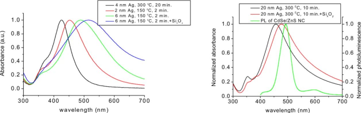
We form silver nanoislands by evaporating on smooth quartz substrates in vacuum environment at very low deposition rates around 0.1-0.2 Å/sec for mass thicknesses < 20 nm. At such slow evaporation rates and low mass thicknesses, the resulting Ag film consists of randomly-distributed nanoislands separated from each other. These metal nanoislands exhibit localized plasmon characteristics. Figure 2 compares the normalized absorption spectra of different Ag nanoislands prepared under different conditions. The larger mass thicknesses cause red-shifted, broader plasmon resonances due to the increasing size of the nanoislands, while annealing the films after evaporation leads to blue-shifted, sharper resonances. Also, the existence of dielectrics with larger refractive indices at the metal interface red-shifts the plasmon resonance. These spectra display the tunability of plasmon resonance as we desire.
533
WN3
11:30 AM – 11:45 AM
To demonstrate the plasmonic resonance coupling of the luminescent nanocyrstals in the proximity of the nanometallic structures, we use the closely-packed CdSe/ZnS NC film and Ag nanoisland film separated by a 10 nm thick silicon oxide layer, which is an important factor to determine the level of plasmonic interaction spatially (since quenching becomes increasingly dominant for spacing shorter than 10 nm). To further investigate the effect of localized plasmons on the spontaneous emission characteristics of these NCs, we also prepare two control groups for comparison: one with the same NCs directly on the identical Ag nanoisland film, and the other only with the same NCs. We carefully tune the plasmonic resonance of the nanosilver film to match well with the emission spectrum of NCs, which is another important factor to determine the level of plasmonic coupling spectrally. We use CdSe/ZnS NCs of 1.9 nm in diameter with a size distribution of ± 5 % and a peak emission wavelength of 492 nm. For this luminescent material, we use Ag nanoislands with a mass thickness of 20 nm annealed at 300 ºC for 10 minutes. Figure 2 displays the absorption spectra of this silver film with and without 10 nm silicon oxide spacer along with the PL spectrum of CdSe/ZnS NCs in film, featuring an excellent spectral overlap with the absorption spectrum of plasmonic silver nanoparticles (which further red-shifts when the NCs are in their proximity, effectively increasing the dielectric constant of the medium). Figure 1 shows the resulting PL peak wavelength of the NC emitters shifted from 492 nm to 506 nm (by 14 nm) and their FWHM reduced from 45 nm to 35 nm (by 10 nm, corresponding to more than 22 % reduction) as a result of the interaction with the nanometallic film. Figure 1 also depicts the
resulting collective photoluminescence spectrum of the sample CdSe/ZnS NCs+SixOy+nanoAg when excited at 325
nm with a He-Cd laser at room temperature, along with those of the control groups. In these PL spectra, despite the random distribution of the closely-packed nanocrystals and silver nanoislands and the resultant spatial fluctuations in their PL, we observe significant enhancement (of 21.6 times) in the ensemble photoluminescence average of
CdSe/ZnS NCs+SixOy+nanoAg with respect to the control group CdSe/ZnS NCs+nanoAg. This is due to the
dominant nonradiative energy transfer, which quenches the NC emission when there is no dielectric spacer, and the dominant radiative energy transfer (Förster-type energy transfer) when there is a spacer of right thickness (thick enough to prevent nonradiative decay and thin enough to utilize the increased optical density of states in the proximity of the plasmonic structures). When compared to the other control group of the same NCs without Ag nanoislands (when there is no plasmonic resonance coupling), the enhancement factor is 15.1-fold, which implies a quenching factor of 0.7 in the case of no spacer. Consequently, the PL enhancement ratio is given as 15.1:1.0:0.7 for NC+SixOy+nanoAg:NC:NC+nanoAg. Furthermore, this corresponds to 12-fold enhancement in the total number of photons collected from the NC emitters in the case of plasmonic coupling compared to no plasmonic resonance. In conclusion, as a proof-of-concept demonstration, we show that the localized plasmons of metal nanoisland films provide the ability to modify and control the collective spontaneous emission of nanocrystals in their proximity (including emission peak wavelength and linewidth in addition to intensity). Using randomly-distributed Ag nanoparticles, we demonstrate plasmonic resonance tuned for the proximal CdSe/ZnS NC emitters to shift PL peak wavelength (by 14 nm) and reduce the FWHM (by 10 nm), while enhancing PL intensity by 15.1 and 21.6 times compared to the control groups of nanocrystals alone and those with nanoAg but no dielectric spacer, respectively.
300 400 500 600 70 0 0.0 0.2 0.4 0.6 0.8 1.0 A bso rb an ce ( a.u .) w avelength (nm ) 4 n m Ag , 30 0 0C , 2 0 m in . 2 nm Ag , 1 50 0C, 2 m in. 6 nm Ag , 1 50 0C, 2 m in . 6 nm Ag , 1 50 0C, 2 m in .+Si xOy 300 400 500 600 700 0.0 0.2 0.4 0.6 0.8 1.0 0.0 0.2 0.4 0.6 0.8 1.0 N orm aliz ed phot olum ines cenc e N o rm aliz ed a b so rbanc e wavelength (nm) 20 nm Ag, 300 0C, 10 m in. 20 nm Ag, 300 0C, 10 m in.+Si xOy PL of CdSe/ZnS NC
Fig. 2. Absorption spectra of Ag with mass thickness of 4 nm annealed at 300ºC for 20 min, Ag(2 nm) 150 ºC 2 min, Ag (6 nm)
150ºC 2 min, Ag (6 nm) 150 ºC 2 min covered with 10 nm-thick SixOy (left) and absorption spectra of Ag (20 nm) annealed at 300 ºC for 10 min and that also covered with 10 nm-thick SixOy along with the photoluminescence spectrum of CdSe/ZnS NCs (right).
Acknowledgements: This work is supported by EU MOON, EU NOE PHOREMOST and TUBITAK 104E114, 106E020, 105E065, and
105E066. H.V.D, I.M.S., and S. N. also acknowledge support from Turkish Academy of Sciences (TUBA GEBIP) and TUBITAK.
References
[1] S. Nizamoglu, et al., Nanotechnology 18, 065709, (2007). [2] D. Alexson, et al., J. Phys.: Con. Matter 17, R637-R656,(2005). [3] P. P. Pompa, et al., Nature Nanotechnology 1, 126-130, (2006).
[4] J.-H. Song, et al., Nano Letters 5, No. 8, 1557-1561, (2005). [5] O. Kulakovich, et al., Nano Letters 2, No. 12, 1449-1452, (2002). [6] K. Ray, et al., J. Am. Chem. Soc. 128, 8998-8999, (2006).