共Received 24 April 2001; revised manuscript received 16 July 2001; published 17 October 2001兲 We experimentally investigated the influence of positional disorder on the photonic band gap, defect char-acteristics, and waveguiding in two-dimensional dielectric and metallic photonic crystals. Transmission mea-surements performed on the dielectric photonic crystals have shown a stop band even if a large amount of disorder was introduced to these structures. On the other hand, the photonic band gap of the metallic crystals was found to be very sensitive to disorder, while the metallicity gap was not affected significantly. We addressed how the transmission characteristics of a cavity were affected in the presence of weak disorder. Since the translational symmetry was broken by disorders, we measured different cavity frequencies when we generated defects at various locations. We also demonstrated the propagation of photons by hopping through coupled-cavity structures in both dielectric and metallic two-dimensional photonic crystals. Effects of weak disorder on guiding and bending of electromagnetic waves through the coupled-cavity waveguides were also investigated.
DOI: 10.1103/PhysRevB.64.195113 PACS number共s兲: 42.70.Qs, 42.60.Da, 74.80.⫺g, 71.15.Ap I. INTRODUCTION
Photonic crystals are periodic dielectric and metallic structures in which the refractive index modulation gives rise to stop bands for electromagnetic共EM兲 waves within a cer-tain frequency range in all directions. In recent years, photo-nic band gap共PBG兲 materials have attracted much attention, and many possible applications of such materials were pro-posed and demonstrated.1,2
PBG materials are considered as the photonic analogues of the semiconductors. Existence of photonic band gaps,3 localization of classical waves in disordered photonic systems,4 defect modes5 are reminiscent of what we ob-served in electronic case. For instance, it is well known that the amorphous semiconductors have similar band gaps com-pared to their crystalline counterparts. Similarly, the exis-tence of photonic gaps does not require long range periodic order in photonic structures.6Therefore, investigation of lo-calization phenomena and disorder effects in PBG materials has a fundamental importance in pure and applied physics.
By introducing a defect into an otherwise perfect photonic crystal, it is possible to create localized EM mode inside the photonic band gap. Photons with certain wavelengths can locally be trapped inside the defect volume. Properties of the cavity modes are reminiscent of the impurity states in a semiconductor.5,7 In the past several years, researchers have proposed various applications based on cavity structures built around photonic crystals such as waveguides,8 –13 lasers,14,15 fibers,16 splitters,17 switches,17–20 and resonant antennas.21
PBG structures also provide a promising tool to control and manipulate the flow of EM waves in integrated optical devices.1Therefore, there is a growing interest in developing photonic crystal-based waveguides which can efficiently guide and bend EM waves either along a line defect共a row
of missing rods兲8 –12 or through coupled cavities.13 In the latter case, which is known as coupled-cavity waveguides 共CCW’s兲,13
the EM waves were tightly confined at each de-fect site, and photons can propagate via hopping due to in-teraction between the neighboring evanescent cavity modes.22,23,13 This type of propagation mechanism was al-ready demonstrated experimentally in 1D 共Ref. 24兲 and 3D 共Refs. 13 and 25兲 dielectric photonic crystals.
Since unintentional positional disorders are always present in the PBG structures, it is important to address the influence of disorders on the photonic band gaps, cavity modes, waveguides, and waveguide bends. Previously, the disorder effects were investigated in one-,26 –28two-,29–36and three-dimensional37– 41photonic structures. However, to our knowledge, there are not any complete experimental studies on investigation of positional disorder effects in 2D dielectric and metallic photonic crystals.
Although the employment of PBG structures made of di-electric materials have been successful in various applica-tions, there are certain advantages of introducing metals to the photonic crystals.42– 47For instance, the metallic photonic crystals have a large forbidden gap that extends from zero frequency up to the plasma frequency.44,47Moreover, the me-tallic PBG structures are almost perfect reflectors in low fre-quency regions.43
The paper is organized as follows. In Sec. II, we first describe the experimental setup and construction of photonic crystals. We then investigate the effect of disorders on the photonic band gaps in 2D dielectric and metallic photonic crystals. Localization length was derived from the transmis-sion measurements. Influence of disorder on defect charac-teristics of single rod removed cavities is presented in Sec. III. In Sec IV, we demonstrate guiding and bending of EM waves through 2D dielectric and metallic CCW’s, and inves-tigate how the positional disorder affects the waveguiding phenomena in these structures.
II. INFLUENCE OF DISORDER ON PHOTONIC BAND GAPS
A. Dielectric photonic crystals
In our experiments, the dielectric photonic crystals were made up of cylindrical alumina rods having radius 1.55 mm and refractive index 3.1 at the microwave frequencies with a lattice constant a⫽1.1 cm. The experimental setup con-sisted of a HP 8510C network analyzer and microwave horn antennas to measure the transmission-amplitude spectra. We measured only transverse magnetic共TM兲 fields in which the incident electric field, E, was parallel to the rods. It is well known that the other polarization, transverse electric 共TE兲, does not produce any photonic band gaps in this frequency range.1
The positional disorder was introduced as follows. Each lattice point, zi, was displaced according to zi→zi⫹rei, where r is the randomness parameter, and is a random variable between关0⫺2兴. Therefore, in this way, the degree of the disorder can be changed by varying the parameter r between 0 and a/4. Figure 1 shows the schematics of peri-odic 共left panel兲 and the disordered 共right panel兲 photonic crystals. In our experiments, we performed the transmission measurements by using five different random configurations for disordered case.
We first performed transmission measurements on the pe-riodic and disordered dielectric crystals. We used two differ-ent values of the disorder parameter r, namely r⫽a/9, and
a/4. The transmission was averaged over five different
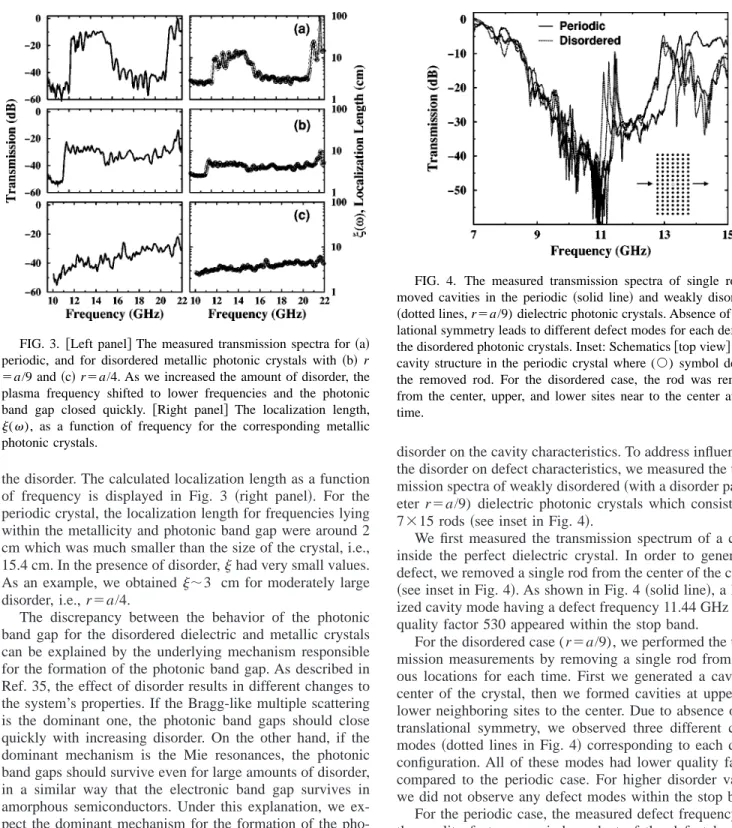
ran-dom configurations for the disordered case. For the periodic case, there appears a stop band extending from 8.67 to 13.25 GHz关Fig. 2共a兲, left panel兴. When we introduced disorder, we observed that 共1兲 the width of the stop band became nar-rower, and共2兲 the upper band edge decreased nearly 15 dB. It was also observed that the photonic band gap persisted even if large amount of disorder was introduced 关Figs. 2共b兲 and 2共c兲, left panel兴. This observation is consistent with the argument that the long-range order is not necessary to achieve stop bands in dielectric photonic crystals.6,35
We also considered frequency dependence of the localiza-tion length which is usually defined as35,34,38
⫺1共兲⫽⫺
具
ln T共兲典
2L , 共1兲
where L⫽15.4 cm is the crystal length and
具
•••典
denotes the ensemble averaging over various configurations. Figure 2 共right panel兲 displayed the calculated localization length by using Eq.共1兲 for 共a兲 the periodic and 共b兲, 共c兲 the disordered cases. For the periodic crystal, while the localization lengths were much smaller than the length of the crystals for the frequencies within the photonic band gap, the localization lengths corresponding to lower and higher transmission bands were larger than the crystal length. On the other hand, the localization length became smaller as we increased the amount of the disorder in disordered crystals 关see Fig. 2共c兲, right panel兴.B. Metallic photonic crystals
Next, we performed the transmission measurements cor-responding to the periodic and disordered metallic photonic crystals. The metallic photonic crystals were constructed from cylindrical copper rods with radius 1.45 mm, and peri-odicity a⫽1.1 cm. Figure 3 共left panel兲 displays the mea-sured transmission spectra as a function of frequency. For the periodic crystal 关see Fig. 3共a兲, left panel兴, we were able to observe the upper band edge of the metallicity gap which extended from 0 GHz to the plasma frequency p ⫽11.67 GHz.42,44,47 We also observed the photonic band
gap that extended from 15.37 to 20.82 GHz due to the peri-odicity of the crystal.44,46
When we introduced disorder to the metallic crystals, we observed two important behaviors. First, the metallicity gap still appeared in the transmission spectrum with a plasma frequency that was shifted to the lower frequencies. Second, the photonic band gap quickly disappeared.32We also inves-tigated how the localization length changed as a function of FIG. 1. Schematic drawing 关top view兴 of the periodic 共left
panel兲 and disordered 共right panel兲 two-dimensional photonic crys-tals. The disorder was introduced by changing the position of lattice points randomly.
FIG. 2. 关Left panel兴 The measured transmission spectra for 共a兲 periodic (r⫽0), and for disordered dielectric photonic crystals with 共b兲 r⫽a/9 and 共c兲 r⫽a/4. The photonic stop band shrank as the amount of disorder was increased. 关Right panel兴 The localization length,(), as a function of frequency for the corresponding pho-tonic crystals. The localization length became smaller than the length of the crystal in the presence of disorder.
the disorder. The calculated localization length as a function of frequency is displayed in Fig. 3 共right panel兲. For the periodic crystal, the localization length for frequencies lying within the metallicity and photonic band gap were around 2 cm which was much smaller than the size of the crystal, i.e., 15.4 cm. In the presence of disorder,had very small values. As an example, we obtained ⬃3 cm for moderately large disorder, i.e., r⫽a/4.
The discrepancy between the behavior of the photonic band gap for the disordered dielectric and metallic crystals can be explained by the underlying mechanism responsible for the formation of the photonic band gap. As described in Ref. 35, the effect of disorder results in different changes to the system’s properties. If the Bragg-like multiple scattering is the dominant one, the photonic band gaps should close quickly with increasing disorder. On the other hand, if the dominant mechanism is the Mie resonances, the photonic band gaps should survive even for large amounts of disorder, in a similar way that the electronic band gap survives in amorphous semiconductors. Under this explanation, we ex-pect the dominant mechanism for the formation of the pho-tonic band gap to be the Bragg scattering in metallic crystals, and the Mie resonances for the dielectric crystals.
III. DEFECT CHARACTERISTICS IN THE PRESENCE OF DISORDER
A. Dielectric photonic crystals
In literature, most of the photonic crystal based applica-tions were built around the cavities which were formed by removing material from otherwise perfect PBG structures. Therefore, it is very important to investigate influence of
disorder on the cavity characteristics. To address influence of the disorder on defect characteristics, we measured the trans-mission spectra of weakly disordered共with a disorder param-eter r⫽a/9) dielectric photonic crystals which consisted of 7⫻15 rods 共see inset in Fig. 4兲.
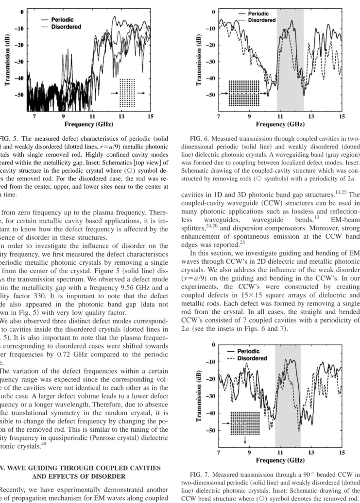
We first measured the transmission spectrum of a cavity inside the perfect dielectric crystal. In order to generate a defect, we removed a single rod from the center of the crystal 共see inset in Fig. 4兲. As shown in Fig. 4 共solid line兲, a local-ized cavity mode having a defect frequency 11.44 GHz and a quality factor 530 appeared within the stop band.
For the disordered case (r⫽a/9), we performed the trans-mission measurements by removing a single rod from vari-ous locations for each time. First we generated a cavity at center of the crystal, then we formed cavities at upper and lower neighboring sites to the center. Due to absence of the translational symmetry, we observed three different cavity modes 共dotted lines in Fig. 4兲 corresponding to each defect configuration. All of these modes had lower quality factors compared to the periodic case. For higher disorder values, we did not observe any defect modes within the stop band.
For the periodic case, the measured defect frequency and the quality factor were independent of the defect location. However, in the presence of positional disorder, depending on the size of the cavity, the resonance frequency shifted towards to lower or higher frequencies. Therefore, the cavity frequency depends on the position of the defect site in the disordered photonic crystals.
B. Metallic photonic crystals
Introducing metallic photonic crystals had certain advan-tages, namely, high rejection ratio, nearly perfect reflectivity at microwave frequencies, and large metallicity gap extend-FIG. 3. 关Left panel兴 The measured transmission spectra for 共a兲
periodic, and for disordered metallic photonic crystals with 共b兲 r ⫽a/9 and 共c兲 r⫽a/4. As we increased the amount of disorder, the plasma frequency shifted to lower frequencies and the photonic band gap closed quickly. 关Right panel兴 The localization length, (), as a function of frequency for the corresponding metallic photonic crystals.
FIG. 4. The measured transmission spectra of single rod re-moved cavities in the periodic共solid line兲 and weakly disordered 共dotted lines, r⫽a/9) dielectric photonic crystals. Absence of trans-lational symmetry leads to different defect modes for each defect in the disordered photonic crystals. Inset: Schematics关top view兴 of the cavity structure in the periodic crystal where (䊊) symbol denotes the removed rod. For the disordered case, the rod was removed from the center, upper, and lower sites near to the center at each time.
ing from zero frequency up to the plasma frequency. There-fore, for certain metallic cavity based applications, it is im-portant to know how the defect frequency is affected by the presence of disorder in these structures.
In order to investigate the influence of disorder on the cavity frequency, we first measured the defect characteristics of periodic metallic photonic crystals by removing a single rod from the center of the crystal. Figure 5 共solid line兲 dis-plays the transmission spectrum. We observed a defect mode within the metallicity gap with a frequency 9.56 GHz and a quality factor 330. It is important to note that the defect mode also appeared in the photonic band gap 共data not shown in Fig. 5兲 with very low quality factor.
We also observed three distinct defect modes correspond-ing to cavities inside the disordered crystals 共dotted lines in Fig. 5兲. It is also important to note that the plasma frequen-cies corresponding to disordered cases were shifted towards lower frequencies by 0.72 GHz compared to the periodic case.
The variation of the defect frequencies within a certain frequency range was expected since the corresponding vol-ume of the cavities were not identical to each other as in the periodic case. A larger defect volume leads to a lower defect frequency or a longer wavelength. Therefore, due to absence of the translational symmetry in the random crystal, it is possible to change the defect frequency by changing the po-sition of the removed rod. This is similar to the tuning of the cavity frequency in quasiperiodic共Penrose crystal兲 dielectric photonic crystals.48
IV. WAVE GUIDING THROUGH COUPLED CAVITIES AND EFFECTS OF DISORDER
Recently, we have experimentally demonstrated another type of propagation mechanism for EM waves along coupled
cavities in 1D and 3D photonic band gap structures.13,25The coupled-cavity waveguide 共CCW兲 structures can be used in many photonic applications such as lossless and reflection-less waveguides, waveguide bends,13 EM-beam splitters,24,20and dispersion compensators. Moreover, strong enhancement of spontaneous emission at the CCW band edges was reported.25
In this section, we investigate guiding and bending of EM waves through CCW’s in 2D dielectric and metallic photonic crystals. We also address the influence of the weak disorder (r⫽a/9) on the guiding and bending in the CCW’s. In our experiments, the CCW’s were constructed by creating coupled defects in 15⫻15 square arrays of dielectric and metallic rods. Each defect was formed by removing a single rod from the crystal. In all cases, the straight and bended CCW’s consisted of 7 coupled cavities with a periodicity of 2a 共see the insets in Figs. 6 and 7兲.
FIG. 5. The measured defect characteristics of periodic 共solid line兲 and weakly disordered 共dotted lines, r⫽a/9) metallic photonic crystals with single removed rod. Highly confined cavity modes appeared within the metallicity gap. Inset: Schematics关top view兴 of the cavity structure in the periodic crystal where (䊊) symbol de-notes the removed rod. For the disordered case, the rod was re-moved from the center, upper, and lower sites near to the center at each time.
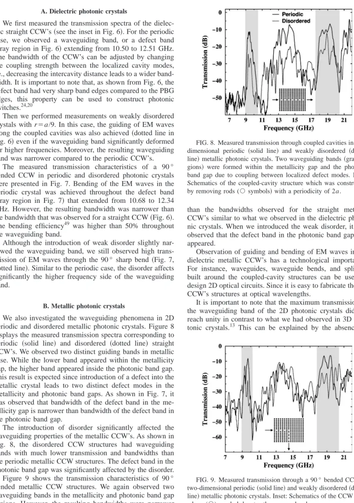
FIG. 6. Measured transmission through coupled cavities in two-dimensional periodic 共solid line兲 and weakly disordered 共dotted line兲 dielectric photonic crystals. A waveguiding band 共gray region兲 was formed due to coupling between localized defect modes. Inset: Schematic drawing of the coupled-cavity structure which was con-structed by removing rods (䊊 symbols兲 with a periodicity of 2a.
FIG. 7. Measured transmission through a 90 ° bended CCW in two-dimensional periodic共solid line兲 and weakly disordered 共dotted line兲 dielectric photonic crystals. Inset: Schematic drawing of the CCW bend structure where (䊊) symbol denotes the removed rod.
width. It is important to note that, as shown from Fig. 6, the defect band had very sharp band edges compared to the PBG edges, this property can be used to construct photonic switches.24,20
Then we performed measurements on weakly disordered crystals with r⫽a/9. In this case, the guiding of EM waves along the coupled cavities was also achieved 共dotted line in Fig. 6兲 even if the waveguiding band significantly deformed for higher frequencies. Moreover, the resulting waveguiding band was narrower compared to the periodic CCW’s.
The measured transmission characteristics of a 90 ° bended CCW in periodic and disordered photonic crystals were presented in Fig. 7. Bending of the EM waves in the periodic crystal was achieved throughout the defect band 共gray region in Fig. 7兲 that extended from 10.68 to 12.34 GHz. However, the resulting bandwidth was narrower than the bandwidth that was observed for a straight CCW共Fig. 6兲. The bending efficiency49 was higher than 50% throughout the waveguiding band.
Although the introduction of weak disorder slightly nar-rowed the waveguiding band, we still observed high trans-mission of EM waves through the 90 ° sharp bend 共Fig. 7, dotted line兲. Similar to the periodic case, the disorder affects significantly the higher frequency side of the waveguiding band.
B. Metallic photonic crystals
We also investigated the waveguiding phenomena in 2D periodic and disordered metallic photonic crystals. Figure 8 displays the measured transmission spectra corresponding to periodic 共solid line兲 and disordered 共dotted line兲 straight CCW’s. We observed two distinct guiding bands in metallic case. While the lower band appeared within the metallicity gap, the higher band appeared inside the photonic band gap. This result is expected since introduction of a defect into the metallic crystal leads to two distinct defect modes in the metallicity and photonic band gaps. As shown in Fig. 7, it was observed that bandwidth of the defect band in the me-tallicity gap is narrower than bandwidth of the defect band in the photonic band gap.
The introduction of disorder significantly affected the waveguiding properties of the metallic CCW’s. As shown in Fig. 8, the disordered CCW structures had waveguiding bands with much lower transmission and bandwidths than the periodic metallic CCW structures. The defect band in the photonic band gap was significantly affected by the disorder. Figure 9 shows the transmission characteristics of 90 ° bended metallic CCW structures. We again observed two waveguiding bands in the metallicity and photonic band gap regions. However, the resulting bandwidths were narrower
than the bandwidths observed for the straight metallic CCW’s similar to what we observed in the dielectric photo-nic crystals. When we introduced the weak disorder, it was observed that the defect band in the photonic band gap dis-appeared.
Observation of guiding and bending of EM waves in 2D dielectric metallic CCW’s has a technological importance. For instance, waveguides, waveguide bends, and splitters built around the coupled-cavity structures can be used to design 2D optical circuits. Since it is easy to fabricate the 2D CCW’s structures at optical wavelengths.
It is important to note that the maximum transmission in the waveguiding band of the 2D photonic crystals did not reach unity in contrast to what we had observed in 3D pho-tonic crystals.13 This can be explained by the absence of FIG. 8. Measured transmission through coupled cavities in two-dimensional periodic 共solid line兲 and weakly disordered 共dotted line兲 metallic photonic crystals. Two waveguiding bands 共gray re-gions兲 were formed within the metallicity gap and the photonic band gap due to coupling between localized defect modes. Inset: Schematics of the coupled-cavity structure which was constructed by removing rods (䊊 symbols兲 with a periodicity of 2a.
FIG. 9. Measured transmission through a 90 ° bended CCW in two-dimensional periodic共solid line兲 and weakly disordered 共dotted line兲 metallic photonic crystals. Inset: Schematics of the CCW bend where (䊊) symbol denotes the removed rod.
confinement of the EM waves along the vertical direction 共along the rod axis兲,50
that resulted in leakage of EM waves along this direction.
V. CONCLUSIONS
In conclusion, we investigated the influence of disorder on photonic band gap characteristics of 2D dielectric and metallic photonic crystals. We observed that positional dis-order had a minor effect on the photonic band gap of the dielectric crystals. For the metallic crystals, the photonic band gap that originated from the periodicity quickly disap-peared in the presence of disorder. However, the metallicity gap persisted even if a large amount of disorder was intro-duced to the crystals. We investigated effect of the disorder on defect characteristics. In disordered photonic crystals, in
which the translational symmetry was absent, the defect fre-quency was changed depending on the position of the defect site. We also reported the observation of guiding and bending of EM waves through coupled cavities in dielectric and me-tallic crystals. Moreover, the influence of disorder on the waveguiding through the coupled-cavity waveguide struc-tures was investigated.
ACKNOWLEDGMENTS
This work was supported by NATO Grant No. SfP971970, National Science Foundation Grant No. INT-9820646, Turkish Department of Defense Grant No. KOBRA-001, and Thales JP8.04. Ames Laboratory is oper-ated for the U.S Department of Energy by Iowa State Uni-versity under Contract No. W-7405-Eng-82.
*Author to whom correspondence should be addressed. Electronic address: [email protected]
1J. D. Joannopoulos, R. D. Meade, and J. N. Winn, Photonic Crys-tals: Molding the Flow of Light 共Princeton University Press, Princeton, NJ, 1995兲.
2
For a recent review, see articles in Photonic Crystal and Light Localization in the 21st Century, edited by C. M. Soukoulis 共Kluwer, Dordrecht, 2001兲.
3K. M. Ho, C. T. Chan, and C. M. Soukoulis, Phys. Rev. Lett. 65, 3152共1990兲.
4S. John, Phys. Rev. Lett. 53, 2169共1984兲; 58, 2486 共1987兲; Phys. Today 44, 32共1991兲.
5E. Yablonovitch, T. J. Gmitter, R. D. Meade, A. M. Rappe, K. D. Brommer, and J. D. Joannopoulos, Phys. Rev. Lett. 67, 3380 共1991兲.
6S. John, in Photonic Band Gap Materials, edited by C. M. Souk-oulis共Kluwer, Dortrecht, 1996兲, p. 563.
7E. Ozbay, G. Tuttle, M. M. Sigalas, C. M. Soukoulis, and K. M. Ho, Phys. Rev. B 51, 13 961共1995兲.
8A. Mekis, J. C. Chen, I. Kurland, S. Fan, P. R. Villeneuve, and J. D. Joannapoulos, Phys. Rev. Lett. 77, 3787共1996兲.
9Shawn-Yu Lin, E. Chow, V. Hietala, P. R. Villeneuve, and J. D. Joannopoulos, Science 282, 274共1998兲.
10B. Temelkuran and E. Ozbay, Appl. Phys. Lett. 74, 486共1999兲. 11A. Chutinan and S. Noda, Phys. Rev. B 62, 4488共2000兲. 12M. Loncar, D. Nedeljkovic, T. Doll, J. Vuckovic, A. Scherer, and
T. P. Pearsall, Appl. Phys. Lett. 77, 1937共2000兲.
13M. Bayindir, B. Temelkuran, and E. Ozbay, Phys. Rev. Lett. 84, 2140共2000兲; Phys. Rev. B 61, R11 855 共2000兲.
14O. Painter, R. K. Lee, A. Scherer, A. Yariv, J. D. O’Brien, P. D. Dapkus, and I. Kim, Science 284, 1819共1999兲.
15A. Mekis, M. Meier, A. Dodabalapur, R. E. Slusher, and J. D. Joannopoulos, Appl. Phys. A: Mater. Sci. Process. 69, 111 共1999兲.
16J. C. Knight, J. Broeng, T. A. Birks, and P. St. J. Russell, Science 282, 1476共1998兲.
17M. Bayindir, B. Temelkuran, and E. Ozbay, Appl. Phys. Lett. 77, 3902共2000兲.
18P. R. Villeneuve, D. A. Abrams, S. Fan, and J. D. Joannopoulos, Opt. Lett. 21, 2017共1996兲.
19R. W. Ziolkowski and M. Tanaka, Opt. Quantum Electron. 31, 843共1999兲.
20S. Lan, S. Nishikawa, and O. Wada, Appl. Phys. Lett. 78, 2101 共2001兲.
21B. Temelkuran, M. Bayindir, E. Ozbay, R. Biswas, M. M. Sigalas, G. Tuttle, and K. M. Ho, J. Appl. Phys. 87, 603共2000兲. 22N. Stefanou and A. Modinos, Phys. Rev. B 57, 12 127共1998兲. 23A. Yariv, Y. Xu, R. K. Lee, and A. Scherer, Opt. Lett. 24, 711
共1999兲.
24M. Bayindir, S. Tanriseven, and E. Ozbay, Appl. Phys. A: Mater. Sci. Process. A72, 117共2001兲; M. Bayindir, S. Tanriseven, A. Aydinli, and E. Ozbay, ibid. 73, 125共2001兲.
25M. Bayindir, E. Ozbay, B. Temelkuran, M. M. Sigalas, C. M. Soukoulis, R. Biswas, and K. M. Ho, Phys. Rev. B 63, 081107共R兲 共2001兲.
26A. R. McGurn, K. T. Christensen, F. M. Mueller, and A. A. Ma-radudin, Phys. Rev. B 47, 13 120共1993兲.
27L. Pavesi and P. Dubos, Semicond. Sci. Technol. 12, 570共1997兲. 28S. A. Bulgakov and M. Nieto-Vesperinas, J. Opt. Soc. Am. A 15,
503共1998兲.
29A. R. McGurn, P. Sheng, and A. A. Maradudin, Opt. Commun. 91, 175共1992兲.
30M. M. Sigalas, C. M. Soukoulis, E. N. Economou, C. T. Chan, and K. M. Ho, Phys. Rev. B 48, 14 121共1993兲.
31M. M. Sigalas, C. M. Soukoulis, C. T. Chan, and D. Turner, Phys. Rev. B 53, 8340共1996兲.
32G. Guida, Opt. Commun. 156, 294共1998兲.
33H. Y. Ryu, J. K. Hwang, and Y. H. Lee, Phys. Rev. B 59, 5463 共1999兲.
34A. A. Asatryan, P. A. Robinson, L. C. Botten, R. C. McPhedran, N. A. Nicorovici, and C. M. de Sterke, Phys. Rev. E 62, 5711 共2000兲.
35E. Lidorikis, M. M. Sigalas, E. N. Economou, and C. M. Souk-oulis, Phys. Rev. B 61, 13 458共2000兲.
36G. Guida, T. Brillat, A. Ammouche, F. Gadot, A. De Lustrac, and A. Priou, J. Appl. Phys. 88, 4491共2000兲.
37M. Stoytchev and A. Z. Genack, Phys. Rev. B 55, R8617共1997兲. 38Yu. A. Vlasov, M. A. Kaliteevski, and V. V. Nikolaev, Phys. Rev.
B 60, 1555共1999兲.
39A. Chutinan and S. Noda, J. Opt. Soc. Am. B 16, 1398共1999兲. 40M. M. Sigalas, C. M. Soukoulis, C. T. Chan, R. Biswas, and K.
Rev. Lett. 76, 2480共1996兲.
45E. Ozbay, B. Temelkuran, M. M. Sigalas, G. Tuttle, C. M. Souk-oulis, and K. M. Ho, Appl. Phys. Lett. 69, 3797共1996兲.
waveguide.
50S. G. Johnson, P. R. Villeneuve, S. Fan, and J. D. Joannopoulos, Phys. Rev. B 62, 8212共2000兲.