Plasmonic Absorbers for Multispectral and Broadband Absorption
Sencer Ayas, Hasan Guner, Burak Turker, Oner Ekiz, Aykutlu Dana
National Institute of Material Science and Nanotechnology
Material Science and Nanotechnology Program, Bilkent University, 06800, Ankara, Turkey
ABSTRACT
We present polarization dependent multispectral and broadband plasmonic absorbers in the visible spectrum. The spectral characteristics of these structures are tunable over a broad spectrum. Experimental results are verified with the FDTD and RCWA analysis methods. These structures are used as surface enhanced raman spectroscopy(SERS) substrates. Designed structures have resonances that span the Raman Stokes and excitation wavelength. Such structures can be used for energy, LED and other spectroscopy applications.
Keywords: absorbers, plasmon, SERS,metamaterial absorbers, coupled modes, fabry-perot mode
1. INTRODUCTION
Plasmonics is one of the emerging fields in the field of nanotechnology and nanophotonics. Due to the fascinating properties of surface plasmons, it has great interest for some applications including surface plasmon sensors[1], plasmonic solar cells[2], negative index metamaterials [3], color filtering[4] and sub diffraction limited imaging[5]. Controlling the efficient absorption of incident light is one of the main goals for most of these applications. Structuring the surface of metallic films is one of the ways to do this where nearly perfect absorption can be obtained. Another way is to use metamaterial absorbers(MAs). MAs is an artificially designed structure, where optical properties are engineered such that impedances of designed structure and medium is matched for certain frequencies. When the impedances are perfectly matched nearly perfect absorption can be obtained. Generally, MAs are composed of a metallic photonic structure that coupled to a thick metallic ground plane through a dielectric layer. One of the main properties of these structures, localized plasmons are excited at the dielectric layer at the resonance frequencies and large field enhancements are possible in this region. Near perfect metamaterial absorbers in the microwave[6], Infrared[7], and near-Infrared[8] frequencies have been experimentally demonstrated. MAs can also be used for surface plasmon sensing platforms where very sharp and near unity resonances are required. Refractive index[9,10] and hydrogen sensing[11] using MAs in the near-infrared and visible frequencies is demonstrated. On the other hand, for some applications, such as solar cells, broadband absorption is more important. If broadband and near unity MAs can be realized, those may be integrated with solar cells and other electrooptical devices. Very recently, broadband and wide angle MA is demonstrated[12] in the visible spectrum where polarization independent and wide angle absorption is obtained using triangular shape plasmonic structures.
In this letter, we report broadband and multispectral polarization dependent MAs in the visible spectrum. Our structure is composed of one dimensional nanowire lamellar grating coupled to a thick metallic layer through a dielectric layer. We realized that rather than using complex two dimensional or more complex multilayer plasmonic structures for multispectral and broadband absorption, simple structures can also be engineered for the same purpose. By tuning only the width of nanowires, we have shown that it is possible to obtain broadband absorption. Even the structures are defined with e-beam lithography, it is very promising compared to other complex MAs for large area fabrication where only the tuning parameter is the width of grating structures. These structures are promising for SERS and spectroscopic applications, where multispectral or broadband field enhancement is important. Also, due to the very thin dielectric layer, these structures can be used for energy applications[13].
2. DESIGN AND SIMULATION
The plasmonic absorber structure is designed to operate over the visible spectrum(400nm-800nm). Silver and Gold are the most popular metals for plasmonic applications. But gold has strong absorption for wavelengths less than 500nm. So that we have used silver for the designed structures. The top and side view of proposed structure is shown in Figure 1.
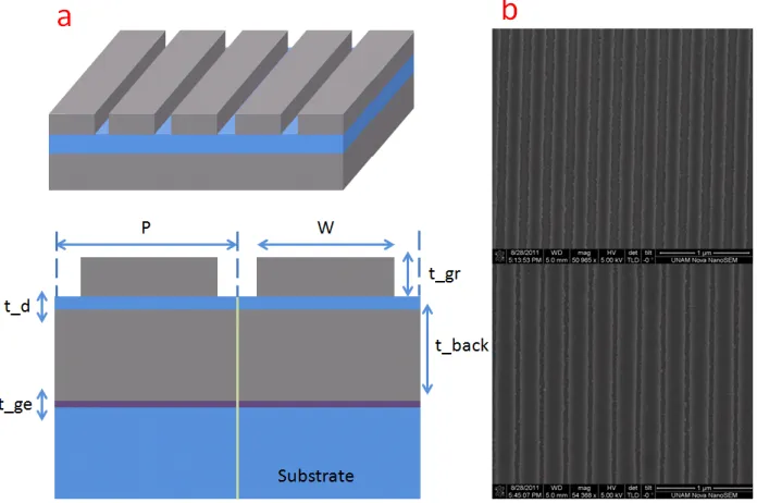
Figure 1.(a)Geometry of proposed structure, P is the period, W is the width of the nanowires, t_d is the thickness of dielectric spacer, t_gr is thickness of nanowires, t_back is the the thickness of supporting metal layer and t_ge is the thickness of germanium layer(b) SEM images of fabricated nanowire plasmonic nanowire metamaterial absorber structures with different nanowire widths.
We choose the thicknesses of dielectric spacer and nanowire grating constant. For all the simulations we assumed a constant dielectric and nanowire thicknesses as t_d=10nm and t_gr=50nm. These values are chosen such that the fabrication of proposed structures are feasible and repeatable. The thickness of back supporting silver layer is 70nm throughout the simulations where it transmits less that 1% of incident light for the specified wavelengths. The period and the duty cycle or the nanowire widths are the only parameters swept in the simulations. In the simulations, germanium layer is neglected, where light transmission through back silver layer is less than 1% of incident light in the 400nm-800nm spectral range. Since the transmitted light is almost zero absorption is calculated as, A(λ)=1-R(λ). Alumina(Al2O3) is used for the dielectric spacer layer. Dielectric function of silver is obtained from the literature[14]. For the alumina, our experimentally characterized dielectric function is used which will be given in the further chapters. The simulations are based on RCWA and FDTD. RCWA is a frequency domain method to simulate the spectral response of periodic structures[15]. The problem domain is divided into small layers. At the boundaries of each layer, electric field and magnetic field are assumed to be continuous. Due to the periodicity, field components can be expressed in terms of fourier expansion. Also incident, transmitted and reflected field components can be written in terms of fourier expansion. Boundary conditions are defined at the interfaces of each layers. By equating tangential components of electric and magnetic fields and their derivatives at each boundary, transmission, reflection and field components in each layer can determined. RCWA method is more accurate for the oblique angles compared to FDTD, where FDTD suffers from high reflection from the boundaries.
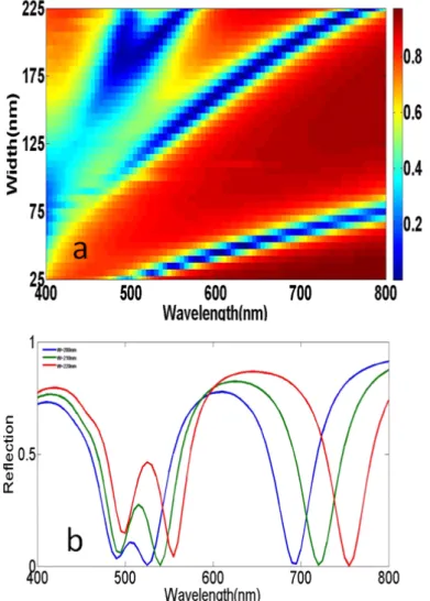
In Figure 2(a), reflection spectra with respect to the width of nanowires is shown. As the width of nanowire width increases above 180nm, the mode starts to split into two separate modes with almost zero reflectance values. For W= 200nm, the absorption bandwidth is about 40nm with near 90% average absorption. For W= 210 and 220nm, resonance modes moves to higher wavelengths. To understand this effect we simulated the magnetic field for these splitted modes. In Figure 3, magnetic field intensities of three resonances(λ=490nm,525nm and 690nm) are shown. For 490nm, the magnetic field is more localized in the gap between nanowires. For 525nm, field is still localized in the gaps but the magnetic field intensity in the dielectric spacer layer increased. For 690nm, magnetic field is localized in the dielectric spacer layer.
Figure 2.(a) Reflection spectra vs width of nanowires or P=250nm. Splitting of low wavelength mode starts around W=180nm (b) Reflection spectra for W=200nm,210nm and 220nm
Shorter wavelength modes can be understood as composite modes of Fabry-Perot and MIM plasmonic modes due to the magnetic field confinement in the gap region[16-17]. When the magnetic field is localized between the nanowires, To further understand the nature of the Fabry-Perot type plasmonic resonances, we simulated the field intensities and dispersion diagram for W=200nm and P=250nm where the thickness of dielectric spacer is zero. In Figure 4(a), dispersion diagram for W=200nm and P=250nm lamellar grating structure is shown. The resonance is around 530nm and it is almost independent of the angle and the magnetic field is localized in the gap region. This kind of response is the nature of Fabry-Perot type plasmon resonances. So that, the double and multispectral resonance characteristic and mode splitting shown in Figure 2(b) is due to the excitation of Fabry-Perot Type Plasmon resonances and the coupling of MIM and Fabry-Perot type plasmon resonances.
Figure 4.(a) Dispersion diagram for W=200nm and P=250nm (b) Magnetic field intensity distribution for λ=530nm, W=200nm and P=250nm
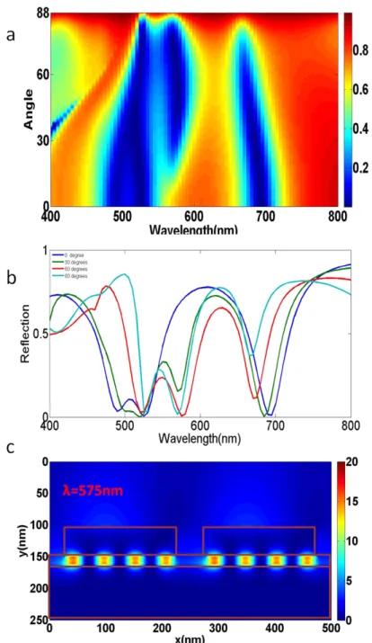
In Figure 5, dispersion diagram of plasmonic metamaterial absorber is shown for W=200nm and P=250nm. From the dispersion diagram, wide angle broadband absorption band is obtained between 490 and 525nm up to 30 degrees. The resonance at 490nm vanishes due to the destructive interference with grating coupled surface plasmon resonance. After, that another resonance is emerged around 570nm and it is angle independent above 30 degrees. This resonance is known as an even MIM mode of plasmonic metamaterial absorber.
Figure 5.(a) Dispersion diagram of plasmonic metamaterial absorber for W=200nm and P=250nm (b) Reflection spectra vs Wavelength for various angle of incidences (c)Magnetic field intensity distribution for λ=575nm and incidence angle=60 o
3. FABRICATION AND CHARACTERIZATION
The SEM image of fabricated structures are as shown in Figure 1(b). Silicon wafer is used as substrate. Germanium, Silver and Alumina(Al2O3) are evaporated using e-beam evaporation. Germanium layer is used to smoothen the roughness of back silver layer. Also it is used as an adhesion layer for the silver. Without Germanium layer the
roughness is less than 3nm. The dielectric function and the thickness of Alumina(Al2O3) is characterized by
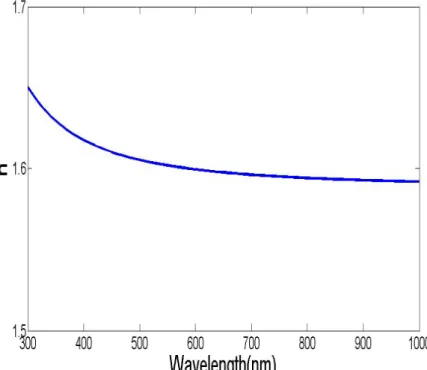
ellipsometer system. The measured thickness of the dielectric is 12nm. Also, the dielectric constant of Alumina(Al2O3) is different than the literature[14, and] it is around 1.6 in the visible spectrum as shown in Figure 6. 30kV E-Beam Lithography system is used to pattern the nanowire arrays. By simply changing the dose, the width of the nanowires are tuned. Final structures are defined with silver E-beam evaporation followed by a subsequent liftoff. Experimental Characterization of the structures are done using a reflection setup as shown in Figure 7(a). Halogen lamp is used as the light source. Light is coupled to a fiber and collimated with a lens. Then using a slit, spot size of the light is reduced. 20x objective is further reduces the spot size to 30um diameter. Reflected light is collected by the same objective and it is coupled to a fiber and sent to the spectrometer. We measured the divergence angle of the beam is about 3 degrees. Since the period of fabricated structures is 250nm, only 0th order reflection is measured which is normal to the surface for the
visible spectrum. Due to the roughness of the silver film, random scattering is unavoidable which is much smaller compared to the diffractive orders. Reflection spectrum is calculated by dividing the reflected light spectrum to a reference spectrum which is the silver film with dielectric spacer on it(Figure 7(b)) for TM polarization only.
Figure 6 Refractive index of Alumina(Al2O3) vs Wavelength. In the simulations refractive index is assumed constant as n=1.6
In Figure 7(b), the reflection spectrum of the fabricated structures is shown and it is compared with the
simulations(Figure 7(c)) where the thickness of the dielectric spacer is assumed 12nm. The widths of the nanowire structures are approximately measured, and they are assumed constant in the simulations(Figure 7(c)). In Figure 7(b), as the width of nanowires increase the resonances shift to higher wavelengths. The noisy spectrum around 400nm is because of the spectrum of the halogen lamp used in the experimental setup. Experimental results are blue shifted compared to the simulations. This might be due to the fabrication imperfection. Such as the cross sections of the nanowire arrays are not exactly rectangular and the dielectric function of the silver does not coincide with the literature values. Although, experiments and simulations are not perfectly matched, multispectral and broadband spectrum characteristics are quite clear. For W=170nm, there is a broad resonance between 450nm and 550nm with an average absorption about 90%. For W=200nm, lower wavelength resonance starts to split into two modes in the simulations. However in the experiment, this is not quite clear which is due to the very noisy spectrum around 400nm.
Figure7.(a) Dispersion Experimental Setup for normal incidence characterization. CL=Collimating lens,BS=Beam Splitters (b) Experimental Reflectivity vs Wavelength for W=170nm, 180nm,190nm, 200nm and P=250nm(c) Simulation Reflectivity vs Wavelength for W=170nm, 180nm,190nm, 200nm and P=250nm and t_d=12nm. We next used these structures as SERS substrates. Recently SERS substrates are demonstrated by strong coupling of localized and grating coupled surface plasmon modes[18]. Due to this coupling, surface and localized plasmon modes separates into two modes. By proper selecting the grating parameter and localized plasmon resonances, structures with resonances at excitation and Stokes wavelengths can be realized. Also, field intensities get stronger due to the strong coupling of these modes. However, designing complex structures with large number of optimization parameters requires excessive effort. On the other hand, structures we have fabricated has only one tuning parameter which is the width of
For 532nm excitation wavelength the Stokes resonances of Raman probe is higher than 532nm and larger periods have to be used. However, from the experimental results, the resonances are broad and goes over 600nm which can be utilized as broadband SERS substrate. For raman measurements, we used 10e-5 Molar Cresyl Violet solution in ethanol as the raman probe. Firstly, samples with nanostructures on it are immersed in the solution for 2 hours. Then the sample is washed with ethanol and dried with nitrogen. The absorption and emission spectrum of Cresyl Violet is shown in Figure 8(a). Witec Alpha 300S NSOM-Raman system with 20x objective is used for raman measurements. The excitation wavelength is 532nm. The power of laser is set between 0.1-0.5mW not to harm the surface of the nanostructures and the integration time for the measurements is 25seconds. In Figure 8(b), raman spectrums of raman probes fabricated nanostructures are shown. Reference spectrum is taken from positions where 50nm thick nanowire silver gratings are replaced by 50nm thick silver film. For the largest peak shown in the raman spectrum, the maximum raman ehancement factor is about 15 fold. For W= 180nm, maximum enhancement factor is obtained. But for other raman peaks,
enhancement factor is higher for W=190nm and W=200nm. Also, The fluorescence is also enhanced more for
W=190nm and 200nm. This is due to the resonances around 600nm as shown in Figure 7(b). The fluorescence peak is shifted to longer wavelength for W=200nm where the resonance is also at longer wavelength.
Figure8.(a) Absorption and Emission Spectrum of Cresyl Violet (b) Relative Raman Spectrum for W=170nm,180nm, 190nm, 200nm and reference
4. CONCLUSION
In conclusion, we have demonstrated wide angle broadband and multispectral plasmonic
metamaterial absorbers in the visible spectrum. The mechanism is based on the coupling of
Fabry-Perot type and MIM plasmonic modes by simply tuning the width of the nanowires. These
structures are easy for large area fabrications. We have also shown that, these structures are
promising as SERS substrates.
REFERENCES
[1] Burak Turker, Hasan Guner, Sencer Ayas, Okan O. Ekiz, Handan Acar, Mustafa O. Guler and Aykutlu Dâna," Grating coupler integrated photodiodes for plasmon resonance based sensing" Lab Chip, 11, 2011
[2] Harry A. Atwater and Albert Polman," Plasmonics for improved photovoltaic devices", Nature Materials, 9, 2010 [3] Stanley P. Burgos, Rene de Waele, Albert Polman, Harry A. Atwater, "A single-layer wide-angle negative-index
metamaterial at visible frequencies", Nature Materials, 9, 2010
[4] Ting Xu, Yi-Kuei Wu, Xiangang Luo, L. Jay Guo,"Plasmonic nanoresonators for high-resolution colour filtering and spectral imaging", Nature Communications
[5] Fang N., Lee H., Sun C., Zhang X., "Sub-diffraction-limited optical imaging with a silver superlens", Science, 308, 2005
[6] N. I. Landy, S. Sajuyigbe, J. J. Mock, D. R. Smith, and W. J. Padilla,"Perfect Metamaterial Absorber", Phys. Rev. Let., 100, 2008
[7] Xianliang Liu, Tatiana Starr, Anthony F. Starr, and Willie J. Padilla," Infrared Spatial and Frequency Selective Metamaterial with Near-Unity Absorbance", Phys. Rev. Let. ,104, 2010
[8] Jiaming Hao, Jing Wang, Xianliang Liu, Willie J. Padilla, Lei Zhou, Min Qiu," High performance optical absorber based on a plasmonic metamaterial", App.Phys. Let., 96, 2010
[9] Na Liu, Martin Mesch, Thomas Weiss, Mario Hentschel, Harald Giessen,"Infrared Perfect Absorber and Its Application As Plasmonic Sensor",Nano Lett., 10 , 2010
[10] Andrea Cattoni, Petru Ghenuche, Anne-Marie Haghiri-Gosnet, Dominique Decanini, Jing Chen, Jean-Luc Pelouard, Stéphane Colli,"λ3/1000 Plasmonic Nanocavities for Biosensing Fabricated by Soft UV Nanoimprint Lithography",
Nano Lett., 11 , 2011
[11] Andreas Tittl, Patrick Mai, Richard Taubert, Daniel Dregely, Na Liu, Harald Giessen,"Palladium-Based Plasmonic Perfect Absorber in the Visible Wavelength Range and Its Application to Hydrogen Sensing", Nano Lett., 11 , 2011 [12] Koray Aydin, Vivian E. Ferry, Ryan M. Briggs, Harry A. Atwater,"Broadband polarization-independent resonant
light absorption using ultrathin plasmonic super absorbers",Nature Communications,2
[13] Fuming Wang and Nicholas A. Melosh ,"Plasmonic Energy Collection through Hot Carrier Extraction", Nano Lett., 11 2011
[14] E.D. Palik, Handbook of Optical Constants of Solids,1997
[15] M. G. Moharam, Drew A. Pommet, Eric B. Grann, T. K. Gaylord,"Stable implementation of the rigorous coupled-wave analysis for surface-relief gratings: enhanced transmittance matrix approach",JOSA A, Vol. 12, Issue 5, 1995 [16] Jin E. Kim, Y.C. Yoon, D.J. Park, Y.H. Ahn, C.Ropers, C.Lienau, J.Kim,Q. H. Park, D.S. Kim,"Fabry-Perot tuning
of the band-gap polarity in a plasmonic crystal",Phys. Rev.B, 75, 2007
[17] X. Jiao, P. Wang, L. Tang, Y. Lu, Q. Li, D. Zhang, P. Yao, H. Ming, J. Xie ,"Fabry-Perot like phenomenon in the surface plasmons resonant transmission of metallic gratings with very narrow slits", ,Appl. Phys. B, 80, 2005 [18] Yizhuo Chu, Mohamad G. Banaee, Kenneth B. Crozier, "Double-Resonance Plasmon Substrates for


![[Nermidil Erner Binark'ın "Şakir Paşa Köşkü-Ahmet Bey ve Şakirleri" adlı kitabının tanıtım haberi]](data:image/gif;base64,R0lGODlhAQABAIAAAP///wAAACH5BAEAAAAALAAAAAABAAEAAAICRAEAOw==)