J. Phys. D: Appl. Phys. 41 (2008) 155317 (10pp) doi:10.1088/0022-3727/41/15/155317
Buffer optimization for crack-free GaN
epitaxial layers grown on Si(111)
substrate by MOCVD
Engin Arslan
1,4, Mustafa K Ozturk
2, Ali Teke
3, Suleyman Ozcelik
2and
Ekmel Ozbay
11 Nanotechnology Research Center–NANOTAM, Department of Physics, Department of Electrical and Electronics Engineering, Bilkent University, 06800 Ankara, Turkey
2 Department of Physics, Faculty of Science and Arts, Gazi University, Teknikokullar, 06500 Ankara, Turkey
3 Department of Physics, Faculty of Science and Letters, Balıkesir University, 10145 Balıkesir, Turkey E-mail: [email protected]
Received 14 April 2008, in final form 19 June 2008 Published 18 July 2008
Online at stacks.iop.org/JPhysD/41/155317
Abstract
We report the growth of GaN films on the Si(111) substrate by metalorganic chemical vapour phase deposition (MOCVD). Different buffer layers were used to investigate their effects on the structural and optical properties of GaN layers. A series of GaN layers were grown on Si(111) with different buffer layers and buffer thicknesses and were characterized by
Nomarski microscopy, atomic force microscopy, high-resolution x-ray diffraction (XRD) and photoluminescence (PL) measurements. We first discuss the optimization of the LT-AlN/HT-AlN/Si(111) templates and then the optimization of the graded AlGaN intermediate layers. In order to prevent stress relaxation, step-graded AlGaN layers were introduced along with a crack-free GaN layer of thickness exceeding 2.6µm. The XRD and PL measurements results confirmed that a wurtzite GaN was successfully grown. The resulting GaN film surfaces were flat, mirror-like and crack-free. The mosaic structure in the GaN layers was investigated. With a combination of Williamson–Hall measurements and the fitting of twist angles, it was found that the buffer thickness determines the lateral coherence length, vertical coherence length, as well as the tilt and twist of the mosaic blocks in GaN films. The PL spectra at 8K show that a strong band edge photoluminescence of GaN on Si (111) emits light at an energy of 3.449eV with a full width at half maximum (FWHM) of approximately 16meV. At room temperature, the peak position and FWHM of this emission become 3.390eV and 58meV, respectively. The origin of this peak was attributed to the neutral donor bound exciton. It was found that the optimized total thickness of the AlN and graded AlGaN layers played a very important role in the improvement of quality and in turn reduced the cracks during the growth of GaN/Si(111) epitaxial layers.
As a substrate for the growth of GaN/AlGaN epitaxial layers, silicon has many advantages as compared with SiC and sapphire due to its high crystal quality, low cost, good electrical and thermal conductivity and large area size [1–7]. 4 Author to whom any correspondence should be addressed.
wafers has attracted considerable academic and commercial attention. However, because of the large mismatches in the latticeparameter(−16.9%)andthermalexpansioncoefficients (approximately 57%) between Si and GaN, cracking occurs along the equivalent {1−100} GaN plane during the cool down [4–11]. Cracking significantly reduces the performance of GaN-based devices due to their current-scattering centres
0022-3727/08/155317+10$30.00 © 2008 IOP Publishing Ltd Printed in the UK
for light propagation as well as poor crystal quality [2]. The growthconditionsandqualityofthecrystalsstronglyaffectthe crack density. The average size of the crack-free surface areas on an epitaxial sample can be increased by manipulating the growth conditions as well as the post-growth heat treatment. However, the appearance of cracks is quite random on the film, whichproducescriticaldifficultiesindeviceapplications. Therefore, the control of the crack distribution in a large area film is the main issue of this study [3–9].
Many methods have been reported to eliminate the cracks and to improve the crystal quality. Kim et al [10] used a five-step graded AlxGa1−xN (
x
= 0.87–0.07) interlayer between an AlN buffer layer and GaN on Si(111). An AlGaN/GaN superlattice was used by Nikishin et al [4] instead of an AlGaN layer, and the insertion of a lowtemperatureAlN(LT-AlN)interlayerintothebulkhighgrowth temperature GaN was reported by Amano et al [8]. However, because of the excessively large thermal expansion coefficient mismatch, these methods have not achieved a perfect crackfree GaN/Si(111) epitaxy when compared with the growth of GaN on the sapphire substrate.
The insertion of a low-temperature AlN (LT-AlN) interlayer into the bulk high growth temperature GaN, which was proposed by Amano et al [8], is considered to be a promising approach to the elimination of cracks for GaN growth on Si(111) substrates. The LT-AlN interlayer can lead to a lower threading dislocation (TD) density, improvement of the crystalline quality and the reduction of tensile stress and cracking that is generated during the high-temperature GaN growth or cooling [12–14,16]. The AlN epitaxial layers are widely applied as nucleation layers (NLs) for GaN growth on silicon and serve not only as wetting layers for GaN but also as barrier layers to prevent Ga meltback etching.
Graded AlGaN intermediate layers between the AlN NL and the GaN introduce compressive stress during growth in order to compensate for the tensile stress that is generated primarily during the cool down from the growth temperature [11]. The growth of a successive AlxGa1−xN layer introduces compressive stress when x < y due to the negative lattice mismatch between GaN and AlN according to [10,13].
The influence of the growth parameters, including the growthtemperature, V/IIIratioandthickness, hasbeenstudied in terms of the crystalline quality of the top GaN layers. However, there have been very few reports on the optimization of HT-AlN and the step-graded AlGaN layers
relating the crystalline quality, surface morphology and stress in the epitaxial GaN layers [11,13].
In this paper, we demonstrate extremely smooth and flat GaN high-quality and nearly crack-free GaN/Si(111) epitaxy. We also discuss the effects of the LT-AlN and HT-AlN template layers’ thicknesses. We investigated the changes in morphologies as a function of the HT-AlN layer thickness. As a next step, the step-graded AlGaN intermediate layers were successfully introduced between the AlN NL and GaN to prevent the cracking of GaN. Then the thickness of the step-graded AlGaN intermediate layers was optimized. We have investigated in detail the effects of the LT-AlN and HT-AlN template layers’ thicknesses on the characteristics of
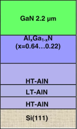
Figure 1. Schematic view of GaN/Si(111) with the HT-AlN/LT-AlN/HT-AlN/AlxGa1−xN buffer system.
the structural features (correlation lengths normal and parallel tothesubstratesurface,tiltandtwist,heterogeneousstrain)and dislocation densities (edge and screw types) by HXRD and the opticalpropertiesbytemperature-dependentPLmeasurements of the hexagonal epitaxial GaN films grown on Si (111).
2. Experimental procedure
GaN epitaxial layers on the Si substrate were grown in a lowpressure metalorganic vapour phase deposition
(MOCVD)
reactor(Aixtron200/4HT-S),usingtrimethylgallium(TMGa), trimethylaluminum (TMAl) and ammonia as Ga, Al and N precursors, respectively. H2 was used as a carrier gas during AlN and AlGaN growth. Before loading the substrates, Si substrates
were sequentially degreased by H2OSO4 :H2O2 :H2O (2:1:1) solutions for 1min and etched in a 2% HF solution for 1min, rinsed in de-ionized water and dried with a nitrogen gun.
At the beginning of the growth of AlN, the substrate was baked in an H2 ambient at 1100◦C for 20min to remove the native oxide. For all the samples, in order to prevent the formation of the amorphous SiNx layer, we carried out Al predeposition on the silicon surface. The buffer structures includedlow-temperature(700◦
C)AlN(LT-AlN)layers,hightemperature (1100◦C) AlN (HT-AlN) layers and a five-step graded AlxGa1−xN interlayer (x = 0.64, 0.54, 0.40, 0.33, 0.22). In all the samples, the GaN layers were
grown at
1050◦C.TheAlNtemplatelayergrowthtemperatureproduces the best crystalline quality and a reasonably low tensile stress in the layer.
FiveGaNsamplesweregrownusingdifferentbufferstructur es (figure 1). The structure of sample A is Si(111)/30nm HT-AlN/30nm LT-AlN/300nm HT-AlN/AlxGa1−xN/GaN. In samples B and C, we used the same buffer structures and changed the HT-AlN layer thickness to 400nm and 500nm, respectively. In all three samples, we used a 700nm AlxGa1−xN interlayer (x = 0.64, 0.54, 0.40, 0.33, 0.22) with different layer thicknesses. The AlGaN layer’s thickness ratio was approximately: 1/1.5/2/2.5/3. In samples D and E, Si(111)/30nm HT-AlN/30nm LT-AlN/400nm HT-AlN/AlxGa1−xN/GaN structures were grown. In these samples
the AlxGa1−xN interlayer thicknesses changed to 800nm and 950nm, respectively. In this study, five different samples were grown with different buffer systems: samples A, B, C, D and E with buffer systems 30nm HT-AlN/30nm LT-AlN/300nm HT-AlN/700nm AlxGa1−xN, 30nm HT-AlN/30nm LT-AlN/400nm HT-AlN/700 AlxGa1−xN, 30nm HT-AlN/30nm
LT-AlN/500nm HT-AlN/700nm AlxGa1−xN, AlN/30nm LT-AlN/400nm HT-AlN/800nm AlxGa1−xN and AlN/30nm LT-AlN/400nm HT-AlN/950nm
AlxGa1−xN, respectively.
The crystalline quality of the GaN layers was examined by high-resolution x-ray diffraction (HRXRD). The x-ray diffraction (XRD) was performed using a Bruker D-8 highresolutiondiffractometersystem,
deliveringCuKα1(1.540Å) radiation, using a prodded mirror and a 4-bounce Ge(220) symmetric monochromator. Data were collected on the (0002), (0004), (0006), (10−15), (20−22), (12−31), (10−11), (10−13) and (11−24) reflections only with ω and ω − 2θ scans. PL measurements were carried out in the temperature range 8–300K with the sample placed in a closedcycle cryostat. A 325nm He–Cd laser with 30mW optical power was used as an excitation source. The luminescence was collected by suitable lenses and then dispersed with a 550mm spectrometer and detected by CCD. The surface morphology was characterized by Nomarski interface contrast optical microscopy and atomic force microscopy (AFM).
3. Results and discussion
We used AlN layers in order to grow III-nitrides on Si(111) surfaces [17]. In order to minimize the disorientation of GaN islands on top, a smooth surface of AlN is required. In our study, we used an HT-AlN interlayer with thicknesses ranging from 300, 400 to 500nm. The crystalline quality, which was characterizedbyHRXRD,improvesandmorestressrelaxation is achieved when the HT-AlN interlayer possesses thicknesses exceeding 400nm. The growth of AlN epitaxial layers starts with Volmer–Weber island growth due to the large lattice mismatch between AlN and the silicon substrate (−17%) [18]. As the thickness of the AlN epitaxial layer increases, the island density is reduced and the size of the islands becomes increasingly larger. When the thickness of the AlN layer reaches 400nm, the surface is nearly smooth and coalesced, which can be then used as a good template for further AlGaN or GaN growth.
Although the AlN/Si(111) template was optimized and a rather low tensile stress in the GaN layer was achieved, the GaN layer still suffered from cracking problems. In order to avoid compressive stress relaxation, seven layers of AlGaN withdifferentcompositionswereintroduced,i.e.theAlcontent wasvariedinsteps. Theseincrementalstepsonlyledtomodest changes in the lattice constant. Therefore, we expected to maintain a pseudo-2D growth mode for each successive layer. This in turn led to a smooth and crack-free GaN surface, as shown in figure 2. We found an optimal value for the total thickness of the step-graded AlGaN intermediate layers. This was achieved by varying the total thickness of these intermediate layers from 700 to 950nm while keeping the thickness ratio constant.
The surface morphologies of all the samples were studied by optical Nomarski interference microscopy. Figures 2(a)– (d) show the Nomarski microscopy (NM) photographs of samples A, B, C, D and E. The variation of the cracks in the samples grown under different conditions is clearly revealed. A nearly crack-free surface was achieved on sample B with a 700nm AlGaN graded interlayer and 400nm HT-AlN layers GaN grown on the silicon substrate. This indicates that the cracks of GaN on Si are seriously affected by the thickness of the AlN and AlGaN buffer.
ThemeasuredcrackdensitiesforsamplesA,B,C,DandE were about 15/cm, 4/cm, 9/cm, 22/cm and 28/cm, respectively. In our case, the crack density increased for those samples with less than 300nm HT-AlN thickness. It also increased above 500nm. In our study, we obtained a completely crack-free 1.9µm GaN layer with a 30nm HT-AlN/30nm LT-AlN/400nm HT-AlN/700nm graded AlxGa1−xN buffer system. The cracks along {1−100} in the GaN layers grown on the Si substrate have been reported by
many groups [10,19].
CracksinGaNonSiareknowntobeformedduringthecooling stage due to a large tensile stress that is caused by the large difference in the thermal expansion coefficients [13–15].
The surface morphology of the GaN layer grown on the step-graded AlGaN intermediate layers is extremely smooth. The root-mean-square (RMS) roughness and the maximum peak-to-valley roughness are between 0.4 and 0.7nm. Figures
3(a)–(e) show a comparison of the surface morphology for samples A, B, C, D and E, respectively. Sample B has a smooth surface with a low rms roughness (rms = 0.4nm)comparedwithsamplesA,C,DandE.Sample
Bwitha700nmgradedAlGaNinterlayershowsfewerdefects, but sample E with a 950nm graded AlGaN interlayer shows structural defects along with a rough morphology, in which similar surface defects have been associated with open core dislocations that have a screw-type component [9,13,43–46].
XRD was performed for all the samples to investigate the crystal phase of the GaN on Si(111). Figure 4 shows the θ scan XRD pattern of a GaN layer grown on a HT-AlN and graded AlxGa1−xN interlayer buffer system. The diffraction patterns exhibited only the dominant wurtzite GaN crystalline (0002), (0004) and (0006) peaks plus two peaks from the Si substrate and a small peak from the AlN buffer layers. For sample B, the (0002), (0004) and (0006) reflections of wurtzite GaN are clearly observed at 34.56◦, 73.02◦ and 126.24◦, respectively. These results indicate a grown GaN layer with the normal orientation along the c-axis of wurtzite crystalline structures [9].
An in-plane scan was also taken by rotating the sample around its surface-normal direction to investigate the in-plane alignment of the GaN film. Figure 5 shows the scan pattern of the (10−11) plane of sample B. It can be seen in figure 5
that diffraction peaks from the (10−11) plane of GaN were observed at 60◦ intervals, confirming the hexagonal structure of the GaN epilayer.
Heteroepitaxial thin films having a large lattice mismatch
with respect to the substrate form a mosaic structure of slightly misoriented sub-grains [20,21,23,24], which is characterized by the nucleation of slightly misoriented islands and the coalescence of these islands towards a smooth surface. The mosaic structure of the epilayers is determined by the size and angular distribution of the mosaic blocks. The vertical and lateral correlation lengths, heterogeneous strain and degree of mosaicity expressed by the tilt and twist angles are important parameters in characterizing the quality of the epitaxial films with a large lattice mismatch to the substrate [20,22,25]. The mosaic blocks are assumed to be slightly misoriented with respect to each other. The out-of-plane rotation of the blocks perpendicular to the surface normal is the mosaic tilt, and the in-plane rotation around the surface normal is the mosaic twist. The average absolute values of the tilt and twist are
directly related to the full width at half maximum (FWHM) of
the corresponding distributions of crystallographic orientations [24,25].
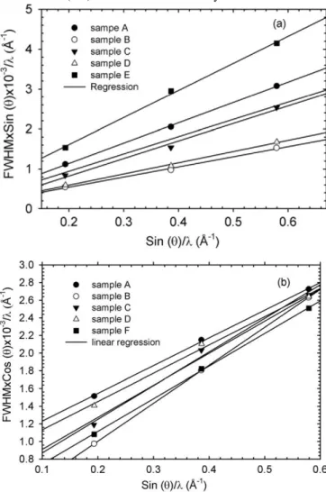
The parameters, vertical and lateral coherence length and tilt angle can be obtained from the Williamson–Hall measurement and the twist angle from an approach that was developed by Srikant et al [25] or from a direct measurement [26], which explains the superposed effect of tilt and twist on the broadening of the FWHMs of off-axis plane rocking curves [27].
Each contribution to the broadening of particular XRD curves can be separated in a Williamson–Hall measurement [20, 27]. Specifically, in triple-axis diffractometer measurements, the broadening of the rocking curve (angular-scan or ω (angular-scan) of the symmetric (0002), (0004) and (0006) reflections for the GaN epitaxial layer is influenced only by Figure 2. Optical Nomarski microscopy views of (a) sample A, (b) sample B, (c) sample C, (d) sample D and (e) sample E.
(c)
(e)
(d)
the tilt angle αtilt and the short coherence length parallel to the substrate surface L.
Separation analogous to the tilt angle αtilt and short
coherence length can be made with a Williamson–Hall plot, when βω(sin θ)/λ is plotted against (sin θ)/λ for each reflection and fitted by a straight line. Then the tilt angle αtilt is obtainedfromtheslopeofthelineardependenceandthelateral coherence length from the inverse of the y-intersection y0 of the fitted line with the ordinate, where is
the FWHM in angular units, θ is the Bragg reflection angle and λ is the x-ray wavelength.
In the radial-scan direction (ω−2θ scan) of the symmetric
reflections (0002), (0004) and (0006), a small vertical correlation length and a heterogeneous strain along the c-axis cause a broadening of the Bragg reflections. These two parameters L⊥ and ε⊥ can similarly be derived from the Williamson–Hall plot. In the Williamson–Hall plot, βω−2θ(cosθ)/λ is plotted against (sin θ)/λ for each reflection and Figure 3. AFM images (2 µm × 2µm scans) of GaN films in (a) sample A, (b) sample B, (c) sample C, (d) sample D and (e) sample E.
(c)
(e)
(d)
again fitted by a straight line. From the y-intersection y0 the vertical correlation length L⊥ can be calculated and the heterogeneous strain ε⊥ can be estimated directly from the slope of the line which is 4ε⊥.
Figure 6 shows the corresponding Williamson–Hall plots for reflections (0002), (0004) and (0006) for triple-axis (a) ω scan and (b) ω − 2θ of all the samples with a different buffer system. The straight lines are linear fits of the experimentaldata. Theexpectedlinearbehaviourofthegraphs
Figure 4. The XRD pattern of all the samples.
Figure 5. Phi scan curve of an asymmetric GaN (10−11) reflection plane for sample B. Every peak shows azimuths of the (10−11) plane. The diffractive peak repeats every 60◦.
is experimentally well confirmed, which gives rather accurate tilt angle values.
The lateral coherence lengths Land tilt angles are shown in table 1. As can be clearly seen, the tilt angles for all the samples were rather small. It can be seen from this table that minimum tilt angle values were obtained for sample B with a 400nm HT-AlN layer and a 700nm AlGaN layer. Furthermore, the same tilt angle values can be obtained for sample D with an 800nm AlGaN buffer layer. The lateral coherence lengths were determined to range from 176 to
1500nm. As seen in table 1, the maximum values were observed for sample B.
The vertical coherence lengths L⊥ values are shown in table 1. The values range from 500 to 1800nm. For sample B, the maximum L⊥ value was 1800nm.
The strain normal to the substrate ε⊥ values obtained for
all the samples is shown in table× 4 to 9.7 × 10⁻⁴. Small
changes were observed for a1. The ε⊥ values range from
8.0 10−
heterogeneous strain with the buffer system thickness. The mean twist angle between the sub-grains can be extrapolated from a fit to the measured double-axis scans data for different (hkl) reflections in a skew symmetric diffraction.
Figure 6. Williamson–Hall plot for GaN layers for all samples. (a) Triple-axis ω scan and (b) triple-axis ω − 2θ scan were measured for the (000l) (l = 2, 4, 6) reflections indicated in the figure. The lines result from a linear fit of the data.
Several extrapolation methods have been reported in the literature for a mean twist angle calculation [20, 25, 28]. However, all these methods include a complicated calculation and fitting procedure for the extraction of the twist angle from the experimental data. On the other hand, Zheng et al [26] proposed a simple empirical approach to obtain the mean twist angle directly without falling into complications.
The FWHM of the rocking curve of an imperfect film is composed of several contributions, such as the mean tilt, twist,theaveragesizeofthesub-grainsandtheinhomogeneous strain distributions. Although the broadening, due to a limited domain size and inhomogeneous strain, can be significant in highly imperfect films, their effects have been eliminated by using a slit of 0.6mm that is placed in front of the detector in double-axis ω scans. Indeed, their contribution to the overall broadening was found to be of minor influence in this measurement case.
In addition, the (0002) reflection and (hkl) reflections with either h or k nonzero orientation of our samples with triple-axis ω − 2θ scans exhibit a small FWHM. The last important point is that the intrinsic width of the reflection for the crystal and the apparatus broadening for all the
angle χ. Therefore, the mean twist angles must be the average value of the FWHMs of scans of χ = 78.6◦.
The measured mean twist angle of the GaN layers is shown in table 1. The mean twist angles change with the HT-ALN layer thickness and the AlGaN layer thickness. The
minimum mean twist angle value was obtained as 0.468◦ for sampleB.ThesampleHT-AlNlayerthicknesswas400nmand the AlGaN buffer layer thickness was 700nm. Based on this observation, it can be argued that the mean twist angle of the GaN epilayers grown on the Si substrate is strongly affected by the HT-AlN layer thickness and the AlGaN layer thickness. It is well known that the GaN epilayers grown on Si(111) in two steps exhibit a high dislocation density [1–7]. There are three main types of dislocations present in the GaN thin film [20,26,29]: the pure edge dislocation with Burgers vector
), the pure screw dislocation with Burgers vector and the mixed dislocation with
. The dislocation density Ddis of GaN films can be calculated from the equations [30,31]
β
(20002) β(21012)
Dscrew = 2, Dedge = 9bedge2 ,
(1)
9bscrew
Ddis = Dscrew + Dedge, (2)
where Dscrew is the screw dislocation density, Dedge is the edge dislocationdensity, β istheFWHMmeasuredbyXRDrocking Table 1. The properties of the GaN layers that were grown with different interlayers are listed. The second and third columns show the HT-AlN and graded AlGaN layer thickness (nm). In the third and fourth columns, the peak position and the FWHM (meV) of the band emission of PL at room temperature are listed. The buffer layer thickness and structural characteristics of all the samples are given, last column shows the rms surface roughness (nm) measured for a 2including the vertical grain size L⊥, lateral grain size L, vertical heterogeneous strain× 2µm2 scan area.ε⊥ parallel to the lattice vector and tilt angle αtilt. The
HT-AlN AlGaN
layer layer PL peak FWHM Twist Tilt Heterogeneous Rms
Sample thickness thickness position of PL angle angle strainroughness
experimentalreflectionsarenegligiblebecausetheseeffects amounttoonlyafewarcsec.Forthisreason,wecanonly measurethebroadeningthatwascausedbythetwistusing ( hkl ) reflectionsinskewgeometry.
TheextendedFWHMsof and scanswereobtained byusingthefitofpseudo-Voigtfunctiontotherockingcurves. TheFWHMofthe scanincreaseswiththeincrementof , whiletheFWHMof scandecreaseswiththeincrementof
[ 26 ] .Theybecomecloserwhenthe (12 31) reflection yields at78.6 .Theseresultsshowedthattherocking-curve widthsof or scansforthishigher anglearecloseto thetwistangles.Ineveryrespect,theFWHMsof scansare largerthanthoseof scanswiththechangeintheinclination
curves and b is the Burgers vector length (bscrew = 0.5185nm, bedge = 0.3189nm).
Figure 7 shows the edge, screw and total dislocation densities for different samples. As seen in this figure, the edge Figure 7. The edge, screw and total dislocation densities for different samples.
andscrewdislocationdensitieschangedwiththeHT-AlNlayer thickness and the AlGaN intermediate layer thickness. It can beseenthatforsampleB,witha400nmHT-AlNtemplatelayer and a 700nm AlGaN intermediate layer thickness, minimum dislocation densities were obtained.
The photoluminescence (PL) spectra at room temperature for all the samples were measured. The PL peak and FWHM values for the five samples are all listed in table 1. The samples show a strong PL emission band between 3.387 and 3.394eV due to the near-band edge emission from wurtzite GaN. The FWHMs of the band edge emission were within the
range 58–
62meV.ThesmallFWHMvaluesofthePLemissionpeaks also indicate a high-quality w-GaN material.
In table 1, the FWHM of the near-band edge emission peak was 58meV for sample B. It indicates that sample B that was grown with a 700nm AlGaN layer and a 400nm HT-AlN layer has the best optical property versus other samples. Theseresultswerecomparedwiththeresultachieved for GaN/Si epilayers [30–32]. The low FWHM values in our films may likely be attributed to the high degree of crystallographic alignment of the buffer layers and to the layers without a grain structure. Jang et al [15] used various Al0.3Ga0.7N/GaN superlattices as an intermediate layer for GaN/Si(111) epitaxial layers, in which their reported values for the FWHM values were 34.49meV.
Figure 8 shows the evolution of PL spectra for sample B over the temperature range 8–300K. As seen in the figure, the
Figure 8. The temperature dependence of the PL spectra and assignment of the peaks for sample B.
PLspectraat8KweredominatedbyaGaNbandedgeemission centred at 3.449eV and its phonon replicas were separated by approximately92meVinsuccessiveorder. TheFWHMofthis main peak is approximately 16meV. At room temperature, the peak position and FWHM of this emission become 3.390eV and58meV,respectively. Theoriginofthispeakwasattributed to the neutral donor bound exciton. These types of transitions arecommonlyresponsibleforthedominantPLlineinundoped and n-type GaN grown by any technique on any substrate. In high-quality strain-free GaN samples with a low concentration of defects, two or more sharp lines that were observed around 3.471eV were attributed to different neutral shallow donor bound exciton transitions [32,33]. In our case, the energy peak position of the main peak redshifted by approximately 18meV compared with a strain-free GaN template, which implies that there is a strong tensile stress present in GaN epilayers grown on Si(111). The shoulder at approximately 3.477eV, which becomes clearer as the temperature increases (see the inset of figure8),wasattributedtotheA-freeexcitontransition[34,35]. Additional defect-related weak blue luminescence (BL) and strong yellow luminescence (YL) peaks at 2.9eV and 2.2eV, respectively, were also observed at the low energy side of the PL spectra at 8K. The YL was attributed to a shallow donor– deep acceptor transition [36]. The deep acceptor is believed to be the native gallium vacancy (VGa), while the shallow donor is attributed to substitutional oxygen (ON) and silicon (SiGa) or C impurities substituted for the nearest neighbour of the Ga sites [37,38]. In our case, VGa–SiGa complexes are believed to be the main cause of the YL band due to the diffusion of Si impurities from the substrate during growth. The BL band peak at approximately 2.9eV in GaN was similar to the notorious YL in this material. The BL band is often observed in undoped, Mg- and Zn-doped GaN with a very similar shape and position [36]. The origin of this peak is not clear in our case, but most probably it is due to the transitions from a deep donor to the MgGa shallow acceptor arising from the residual memory effect of the MOCVD system.
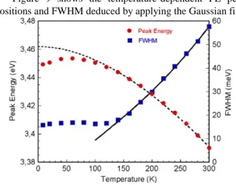
Figure 9 shows the temperature-dependent PL peak positions and FWHM deduced by applying the Gaussian fit
Figure 9. The temperature induced a shift in the energy peak positions of GaN band edge emission together with its FWHM deduced by using Gaussian fits to the PL spectra shown in figure
8. The dashed line and the full circles are drawn by using Varshni's equation (equation (3)) and the solid line is drawn using equation (4).
to the experimental data. The temperature dependence of the peak positions of the GaN band edge emission can be fitted by using Varshni’s equation;
, (3)
where Eg(T) is the transition energy at temperature T , Eg(0) the corresponding energy at 0K and α and β are knownasVarshni’sthermalcoefficientandDebyetemperature, respectively. The best fitted values of α and β are 0.92meVK−1 and 867K, respectively. These values are similar to those reported by Calle et al [34] for the free exciton transition of GaN grown on the Si (111) substrate. As seen in the figure, although the energy peak position of the band edge emission line follows the typical temperature dependence of the energy gap shrinkage over 80K, it deviates from Varshni’s equation at low temperatures. As the temperature increases from 8 to 80K, the peak energy blueshifts by approximately 6meV. This blueshift in the peak position can be interpreted by considering the thermal dissociation of the main bound exciton to other shallower donor bound excitons, which could notberesolvedduetothelimitedlinewidthofthePLspectrum. Similar behaviour was also observed by Zhang et al [39]. The thermal dissociation of the main bound exciton to free excitons and other shallower donor bound excitons is also accompanied by a change in the relative intensities of these transitions with increasing temperature [40].
Figure 9 also shows the temperature dependence of the FWHM of the main peak. A study of the linewidth of excitons provides information about the scattering mechanisms [41]. Temperature-independent inhomogeneous and homogeneous broadeningmechanismsrelatedtovariousscatteringprocesses such as phonons or excitons can be considered for the observed behaviour of the linewidth. Since the excitation power density of the current measurements is approximately 5mWcm−2 the exciton–exciton interaction can be ignored. If we assume that the linewidth is mainly related to the exciton broadening through phonon scattering, it can be described by
Figure 10. GaN band edge related PL intensity as a function of inverse temperature and the temperature dependence of the relative intensities (IBE/IYL). The solid line is drawn to calculate the activation energies by using equation (5). The dashed line represents the exponential fit to the temperature behaviour of the IBE/IYL ratio.
the expression [41]
LO
FWHM(T)
where subscripts I and H refer to inhomogeneous and homogeneous broadening and γac and LO are parameters describing the exciton–phonon interactions. It is clearly observed that the FWHM increases with temperature at two different rates. At low temperatures homogeneous broadening is determined by the scattering of excitons by acoustic phonons, which shows a monotonic increase in the FWHM.
At hightemperaturestheexciton–
LOphononinteractionbecomes the dominant mechanism since the density of LO phonons increases as the temperature increases. Indeed, fitting the experimental data using equation (4) above the temperature of 120K gives an excellent correlation indicating that the main contribution to the observed FWHM is the exciton–phonon interaction.
Figure 10 shows an Arrhenius plot of the PL intensity for band edge emission over the temperature ranges under investigation. As shown in the figure, the PL intensity of the emission decreases as the temperature increases. The dominant mechanism leading to this thermal quenching of PL intensity is due to the increase in the effects of the nonradiative recombination centres with temperature. As seen in the figure, the PL intensity decreases rather little at low temperatures but decreases more rapidly at high temperatures. This suggests that there are two different mechanisms that are responsible in the low- and high-temperature regimes. The activation energies in these thermally activated processes were calculated using the following equation [42]:
, (5) where Eai is the activation energy of the corresponding nonradiative recombination centres, αi is the process rate parameter and kB is Boltzmann’s constant. The fitted curve is shown as the solid line in figure 10. The thermal activation energies of 6meV for the low-temperature and 50meV for the high-temperature regimes were deduced from the best fit by considering the bi-exponential function. At low temperatures, the thermal quenching of the PL peak intensity with 6meV activation energy could be related to the thermal dissociation of the main donor bound exciton line at 3.449nm into other shallower donors as discussed in the temperature dependence of the emission peak. A faster decreasing rate of PL intensity with 50meV thermal activation energy is related to the increase in nonradoative recombination centres as the temperature increases. The temperature dependence of the relative intensities of the GaN band edge emission with respect to the YL (IBE/IYL) is also shown in figure 10. This ratio decreases with temperature and becomes less than 1 at room temperature indicating that the defect density in this sample is most probably due to the intensive diffusion of Si impurities from the Si substrate to the GaN epilayer.
4. Conclusions
Inthisstudy, theinfluenceoftheHT-AlNbufferlayerthickness in the range from 300 to 500nm and the AlGaN buffer layer thicknessintherangefrom700to950nmontheGaNlayerwas investigated. Single crystalline GaN films were successfully grown on Si(111) substrates by MOCVD. The thicknesses of the GaN epitaxial layers exceeded 2.6µm. The evolution of the surface morphology of GaN films as a function of the HT-AlN thickness was investigated. Crack-free flat GaN films were obtained with a 400nm HT-AlN layer. Nearly crack-free GaNepitaxiallayerswereachievedbyintroducingstep-graded AlGaN intermediate layers on optimized HT-AlN/Si(111) templates. The crystalline quality and morphology of the GaN layers significantly improved after the insertion of stepgraded AlGaN layers. We found that stress relaxation due to the step-graded AlGaN layers was also dependent on the layer thickness. Thestep-gradedAlGaNlayersweregrowntoatotal thickness of 700nm. The edge and screw dislocation density changed with the HT-AlN layer thickness and the AlGaN intermediate layer thickness. For sample B, with a 400nm HT-AlNtemplatelayeranda700nmAlGaNintermediatelayer thickness, minimum dislocation densities were obtained.
At room temperature, the samples show a strong PL emission band between 3.387 and 3.394eV due to the nearband edge emission from wurtzite GaN. The FWHMs of the band edge emission were within the range 58–62meV. The small FWHM values of the PL emission peaks also indicate high-quality w-GaN material. The FWHMs of the near-band edge emission peak were 58meV for sample B that was grown
with a 700nm AlGaN layer and a 400nm HT-AlN layer which has the best optical property of all the samples.
Acknowledgments
This work is supported by the European Union under the projects METAMORPHOSE, PHOREMOST, EU-PHOME, EU-ECONAM and TUBITAK under Project Numbers 105E066, 105A005, 106E198, 106A017. One of the authors (EO) also acknowledges the partial support from the Turkish Academy of Sciences.
References
[1] Pal S and Jacob C 2004 Bull. Mater. Sci. 27 501
[2] Krost A and Dadgar A 2002 Phys. Status. Solidi a 194 361 [3] Krost A and Dadgar A 2002 Mater. Sci. Eng. B 93 77 [4]
Nikishin S A, Faleev N N, Antipov G, Francoeur S, Grave de Peralta L, Seryogin G A, Temkin H, Prokofyeva T I, Holtz M and Chu S N G 1999 Appl. Phys.
Lett. 75 2073
[5] Gokkavas M, Butun S, Tut T, Biyikli N and Ozbay E 2007 Photon. Nanostruct. 5 53
[6] Butun B, Cesario J, Enoch S, Quidant R and Ozbay E 2007 Photon. Nanostruct. 5 86
[7] Yu H, Ozturk K M, Ozcelik S and Ozbay E 2006 J. Cryst. Growth 293 273
[8] Amano H, Iwaya M, Hayashi N, Kashima T, Katsuragawa M, Takeuchi T, Wetzel C and Akasaki I 1999 J. Nitride Semicond. Res. 4S1 G10.1
[9] Yu J W, Lin H C, Feng Z C, Wang L S, Tripaty S and Chua S J
2006 Thin Solid Films 498 108
[10] Kim M-H, Do Y-G, Kang H C, Noh D Y and Park S-J 2001 Appl. Phys. Lett. 79 2713
[11] Ishikawa H, Zhao G Y, Nakada N, Egawa T, Soga T, Jimbo T and Umeno M 1999 Phys. Stat. Sol. (a) 176 599
[12] Able A, Wegscheider W, Engl K and Zweck J 2005 J. Cryst. Growth 276 415
[13] Cheng K, Leys M, Degroote S, Van Daele B, Boeykens S, Derluyn J, Germain M, Van Tendeloo G, Engelen J and
Borghs G 2006 J. Electron. Mater. 35 592
[14] Raghavan S and Redwing J M 2005 J. Appl. Phys. 98 023514 [15] Jang S-H and Lee C-R 2003 J. Cryst. Growth 253 64 [16] Mastro M A, Eddy C R Jr, Gaskill D K, Bassim N D, Casey J,
Rosenberg A, Holm R T, Henry R L and Twigg M E 2006 J. Cryst. Growth 287 610
[17] Dadgar A, Blasing J, Diez A, Alam A, Heuken M and Krost A¨
2000 Japan. J. Appl. Phys. 39 L1183
[18] Wu C-L, Chou L-J and Gwo S 2004 Appl. Phys. Lett. 85 2071 [19] Hageman P R, Haffouz S, Kirilyuk V, Grzegorczyk A and
Larsen P K 2001 Phys. Status Solidi a 188 523
[20] Metzger T, Hoppler R, Born E, Ambacher O, Stutzmann M,¨ Stommer R, Schuster M, G¨ obel H, Christiansen S,¨
Albrecht M and Strunk H P 1998 Phil. Mag. A 77 1013 [21] Heying B, Wu X H, Keller S, Li Y, Kapolnek D, Keller B P,
DenBaars S P and Speck J S 1995 Appl. Phys. Lett. 68 643 [22] Vickers M E, Kappers M J, Datta R, McAleese C,
J. Phys. D: Appl. Phys. 38 A99
[23] Weimann N G and Eastman L F 1998 J. Appl. Phys. 83 3656 [24] Holy V, Kubena J, Abramof E, Lischka K, Pesek A and
Koppensteiner E 1993 J. Appl. Phys. 74 1736 [25] Srikant V, Speck J S and Clarke D R 1997 J. Appl. Phys. 82 4286 [26] Zheng X H, Chen H, Yan Z B, Han Y J, Yu H B, Li D S,
Huang Q and Zhou J M 2003 J. Cryst. Growth 255 63 [27] Williamson G K and Hall W H 1953 Acta Metall. 1 22 [28] Sun Y J, Brandt O and Ploog K H 2003 J. Mater. Res. 18
1247
[29] Sasaki H, Kato S, Matsuda T, Sato Y, Iwami M and Yoshida S
2007 J. Cryst. Growth 298 305
[30] Gay P, Hirsch P B and Kelly A 1953 Acta Metall. 1 315 [31] Dunn C G and Koch E F 1957 Acta Metall. 5 548 [32]
Reshchikov M A, Huang D, Yun F, He L, Morkoc¸ H, Reynolds D C, Park S S and Lee K Y 2001 Appl. Phys. Lett.
79 3779
[33] Freitas J A Jr, Moore W J, Shanabrook B V, Braga G C B, Lee S K, Park S S and Han J Y 2002 Phys. Rev. B 66 233311
[34] Calle F, Sanchez F J, Tijero J M G, Sanchez-Garcia M A, Calleja E and Beresford R 1997 Semicond. Sci. Technol.
12 1396
[35] Tu L W, Lee Y C, Stocker D and Schubert E F 1998 Phys. Rev. B 58 10696
[36] Reshchikov M A and Morkoc¸ H 2005 J. Appl. Phys. 97 061301 [37] Neugebauer J and Vande Walle C G 1996 Appl. Phys. Lett.
69 503
[38] Mattila T and Nieminen R M 1997 Phys. Rev. B 55 9571 [39] Zhang J X, Qu Y, Chen Y Z, Uddin A, Chen P and Chua S J
2007 Thin Solid Films 515 4397
[40] Viswanath A K, Lee J I, Yu S, Kim D, Choi Y and Hong C H 1998 J. Appl. Phys. 84 3848
[41] O’Neill M, Oestreich M, Ruhle W W and Ashenford D E 1993 Phys. Rev. B 48 8980
[42] Dean P J 1967 Phys. Rev. B 157 655
[43] Rinaldi R, Antonaci S, Anni M, Lomascolo M, Cingolani R, Botchkarev A and Morkoc H 1999 Phys. Status Solidi b 216 701
[44] Gangopadhyay S, Schmidt T and Falta J 2006 Phys. Status Solidi b 243 1416
[45] Brazel E G, Chin M A and Narayanamurti V 1999 Appl. Phys. Lett. 74 2367
[46] Zheng L X, Xie M H, Seutter S M, Cheung S H and Tong S Y 2000 Phys. Rev. Lett. 85 2352
![Figure 9 also shows the temperature dependence of the FWHM of the main peak. A study of the linewidth of excitons provides information about the scattering mechanisms [41]](https://thumb-eu.123doks.com/thumbv2/9libnet/5619142.111257/10.892.475.816.98.388/temperature-dependence-linewidth-excitons-provides-information-scattering-mechanisms.webp)
