COUPLED PLASMONIC STRUCTURES
FOR SENSING, ENERGY AND
SPECTROSCOPY APPLICATIONS
A DISSERTATION SUBMITTED TO
THE GRADUATE SCHOOL OF ENGINEERING AND SCIENCE OF BILKENT UNIVERSITY
IN PARTIAL FULFILLMENT OF THE REQUIREMENTS FOR THE DEGREE OF
DOCTOR OF PHILOSOPHY IN
MATERIALS SCIENCE AND NANOTECHNOLOGY PROGRAM
By
Sencer Ayas
I certify that I have read this thesis and that in my opinion it is fully adequate, in scope and in quality, as a thesis of the degree of Doctor of Philosophy.
………. Assist. Prof. Dr. Aykutlu Dana (Advisor)
I certify that I have read this thesis and that in my opinion it is fully adequate, in scope and in quality, as a thesis of the degree of Doctor of Philosophy.
………. Assist. Prof. Dr. Necmi Biyikli
I certify that I have read this thesis and that in my opinion it is fully adequate, in scope and in quality, as a thesis of the degree of Doctor of Philosophy.
………. Assoc. Prof. Dr. Ozgur Oktel
I certify that I have read this thesis and that in my opinion it is fully adequate, in scope and in quality, as a thesis of the degree of Doctor of Philosophy.
………. Assoc. Prof. Dr. Hamza Kurt
I certify that I have read this thesis and that in my opinion it is fully adequate, in scope and in quality, as a thesis of the degree of Doctor of Philosophy.
………. Assist. Prof. Dr. Mehmet Solmaz
Approved for the Graduate School of Engineering and Science:
………. Prof. Dr. Levent Onural Director of the Graduate School
ABSTRACT
COUPLED PLASMONIC STRUCTURES FOR SENSING, ENERGY
AND SPECTROSCOPY APPLICATIONS
Sencer Ayas
Ph.D. in Material Science and Nanotechnology Program Supervisor: Assist. Prof. Dr. Aykutlu Dana
August, 2015
Recent advances in nanofabrication and characterization methods have enabled the study of novel optical phenomena, thus boosting the research in nanophotonics and plasmonics. Metal nanostructures offer a route for the excitation of surface plasmons by confining the light in sub-wavelength dimensions, yielding extremely high electromagnetic field intensities. Moreover, coupling different plasmon modes offers a rich optical dispersion which cannot be obtained inherently by using single plasmonic resonator. In this thesis, we first present a detailed study of simple coupled plasmonic structures based on metal-insulator-metal structure. Then, we use similar structures to devise novel optical platforms in various applications such as surface enhanced Raman spectroscopy (SERS), surface enhanced infrared absorption spectroscopy (SEIRA) and plasmon enhanced hot-electron devices.
The first part of this thesis concentrates on coupled plasmonic structures and their spectroscopy and photodetector applications. Firstly, we study these structures numerically and analytically and show surface enhanced Raman spectroscopy (SERS) as a possible application with uniform signal intensities over large areas. Then, fabricating these plasmonic surfaces with sub-10nm gaps over large areas lead to development of single molecule Raman spectroscopy platforms. As an energy related application, a contact free characterization method is developed to probe hot electrons where similar coupled plasmonic surfaces are employed as hot electron devices. Finally, using aluminum and its native aluminum oxide hierarchical plasmonic surfaces are fabricated and its spectroscopy applications are demonstrated.
In the second part of, we develop interference-coating-based sensing platforms in the visible and infrared wavelengths. Despite large field enhancements, plasmonic
structures suffer from low signal intensities due to low mode volumes. To overcome this issue we propose another strategy, namely using interference coatings with small and uniform electric field enhancements over large mode volumes. These surfaces outperform the conventional plasmonic surfaces when they are used as infrared absorption spectroscopy platforms. Finally, similar surfaces are employed as colorimetric sensor platforms to sense monolayer and bilayer proteins simply by change in the surface color.
Keywords: Surface plasmons, coupled plasmons, spectroscopy, hot-electrons, interference coatings, optical sensors
ÖZET
Eşlenmiş Plazmonik Yapıların Sensör, Enerji ve Spektroskopi
Uygulamaları
Sencer Ayas
Malzeme Bilimi ve Nanoteknoloji Programı, Doktora Tez Yöneticisi: Assist. Prof. Dr. Aykutlu Dana
Ağustos, 2015
Nanofabrikasyon ve karakterizasyon metotlarındaki yeni gelişmeler yenilikçi optik çalışmaları hızlandırmış, bu da nanofotonik ve plazmonik çalışmalarında ciddi bir artışa sebep olmuştur. Metal nano-yapılar ışığı dalga boyundan çok küçük boyutlara hapsederek yüzey plazmonlarının uyarılması sağlayarak elektromanyetik alan şiddetini arttırmaktadır. Diğer yandan, farklı plazmon modlarının eşlenmesi tek plazmonik rezonatör yapısıyla elde edilemeyecek çok zengin bir optik bant yapısı sunmaktadır. Bu tezde, ilk olarak metal-dielektrik-metal rezonatör yapısı baz alınarak eşlenik plazmon yapıları detaylı olarak çalışılmıştır. Sonra, benzer yapılar kullanılarak yenilikçi optik platformlar üretilerek yüzey artırımlı Raman spektroskopisi (SERS), yüzey artırımlı kızılötesi emilim spektroskopisi (SEIRA) ve plazmon artırımlı sıcak elektron aygıt uygulamaları gösterilmiştir.
Tezin ilk kısmı plazmonik yapılar ve bu yapıların spektroskopi ve fotodetektör uygulamalarına yoğunlaşmıştır. İlk olarak, bu yapıları analitik ve numerik olarak çalışarak geniş alanlarda sabit artırımlı SERS uygulaması gösterilmiştir. Sonra, benzer yapıların 10nm'den küçük aralıklı olarak üretilmesiyle tek molekül Raman spektroskopisi uygulaması gösterilmiştir. Enerji uygulaması olarak da benzer eşlenik plazmonik yapıları kullanılarak sıcak elektronların ölçüldüğü XPS tabanlı bir yöntem geliştirilmiştir. Son olarak da aluminyum ve doğal aluminyum oksit tabakası kullanılarak hiyerarşik plazmonik yapıları üretilerek spektroskopi uygulamaları gösterilmiştir.
Tezin ikinci kısmında görünür ve kızılötesi dalga boylarında girişim kaplamasına dayanan sensör platformları geliştirilmiştir. Plazmonik yapılar elektromanyetik alan şiddetini çok fazla arttırmalarına rağmen, moleküllerin sinyal şiddetleri mod
hacminin küçüklüğünden dolayı azdır. Bu problemi aşmak için yeni girişim kaplamalara dayalı yeni bir strateji önerilmektedir. Bu yüzeyler kızılötesinde kullanıldıklarında plazmonik yüzeylerden daha iyi performans göstermektedirler. Son olarak da benzer yüzeyler görünür bölgede tek ve çift tabakalı proteinleri renk değişimine bağlı olarak tespit etmek için önerilmektedir.
Anahtar kelimeler: Yüzey plazmonları, eşlenik plazmonlar, spektroskopi, sıcak elektronlar, girişim kaplamaları, optik sensörler
Acknowledgement
I would like to thank my PhD advisor Aykutlu Dâna for accepting me as a PhD student in his group. This thesis would not be successful without his efforts, guidance and support. I have learnt a lot from him; mathematical modeling, coding and tips about clean room processes are few of them. I wouldn't ask for a better advisor.
I would like to thank Prof. Salim Çıracı for accepting me to PhD program.
I would like to thank my thesis committee; Assist. Prof. Necmi Bıyıklı, Assoc. Prof. Mehmet Özgür Oktel, Assist. Prof. Mehmet Ertuğrul Solmaz and Assoc. Prof. Hamza Kurt.
I would like to thank some of my present and past group members; Dr. Gökhan Bakan, Dr. Kemal Çelebi, Hasan Güner, Andi Çupallari, Mustafa Ürel, Ahmet Emin Topal and Serkan Karayalçın. I would especially thank Gökhan and Kemal for being good friends and editing this thesis' drafts. I want to thank Andi for being good friend and companion. He is one of the handy people I have known who made things happen easily; especially clean room processes. I want to thank Mustafa for AFM roughness measurements. I would like to thank Mehmet Kanık for FTIR measurements, graphical illustrations and for being a good friend.
I want to thank Mehmet Ertuğrul Solmaz for partially supporting me for the last 8 months of my PhD.
I would like to thank clean room engineers and technicians; particularly Semih Yaşar, Murat Dere and Mustafa Güler.
I greatly acknowledge TUBITAK through grant 111M344.
Finally, I thank my family for encouraging and supporting me to complete my PhD work.
Contents
ABSTRACT ... iv
ÖZET ... vi
Acknowledgement ... viii
Contents ... ix
List of Figures ... xii
List of Tables ... xxv
Chapter 1 Introduction ... 1
Chapter 2 Well-Defined Coupled Plasmonic Structures ... 7
2.1. Surface Plasmons at Metal-dielectric Interface ... 8
2.2. Surface Plasmons in Metal-Insulator-Metal Resonators ... 11
2.3. Raman Enhancement on a Broadband Meta-surface ... 13
2.3.1. Introduction ... 13
2.3.2. Description of the Plasmonic Meta-Surface ... 14
2.3.3. Coupled Meta-Atoms and Meta-Molecules ... 17
2.3.4. Experimental Results ... 21
2.3.5. Discussion of Spatial Uniformity of Enhancement at the Nanoscale 24 2.4. Edge Rounding Induced Broadband Plasmonic Metamaterial Absorber Structures ... 27
2.5. Conclusion ... 34
Chapter 3 Nano-particle Based Large Area Broadband Plasmonic Surfaces and Their Applications ... 35
3.1. Large Area Plasmonic Metasurfaces ... 36
3.2. Single Molecule Raman Events Using Large Area Plasmonic Surfaces .... 40
3.2.1. Observation of Single Molecule Raman Events Using Smart Phone's Camera 42 3.3. Probing Hot-electron Effects in Wide Area Plasmonic Surfaces Using XPS ... 48
3.3.1. Introduction ... 48
3.3.2. Results ... 49
3.4. Conclusion ... 55
Chapter 4 Exploiting Native Aluminum Oxide for Multispectral Aluminum Plasmonics 56 4.1. Introduction ... 57
4.2. Native Oxide Based Plasmonic Meta-surfaces... 58
4.3. Nanoparticle Based Large Area Surfaces ... 64
4.4. Surface Enhanced Infrared Absorption (SEIRA) Spectroscopy and Surface Enhanced Raman Spectroscopy (SERS) Using Hierarchical Plasmonic Surfaces 67 4.5. All Aluminum Hierarchical Surfaces in the Infrared ... 75
4.6. Conclusion ... 82
Chapter 5 ... 83
Interference Coating Based Sensing Platforms ... 83
5.1. Thermally Tunable Ultrasensitive Vibrational Spectroscopy Platforms Based on Thin Phase Change Films ... 83
5.1.1. Introduction ... 84
5.1.2. Results ... 86
5.2. Strong Interference Based Colorimetric Sensors ... 99
5.2.1. Introduction ... 99
5.2.2. Results ... 101
5.2.3. Protein Binding Experiment ... 106
5.3. Conclusion ... 107
Chapter 6 ... 109
Conclusion ... 109
Bibliography ... 111
Appendix A ... 135
A.1. Effective index simulation in MIM geometry ... 135
A.2. Field Profile Simulation in Multilayer Coatings ... 136
List of Figures
Figure 2-1 Surface plasmon excitation scheme at metal-dielectric interface. ... 8 Figure 2-2. Dispersion relation of surface plasmons at metal-air interface (Solid blue curve). Dispersion of photons in air and glass are shown with solid and dashed red curves. ... 10 Figure 2-3. Surface plasmon excitation scheme for Kretchmann geometry (a) and angular reflectance spectrum for λ=600nm (b). ... 10 Figure 2-4. Geometry of metal-insulator-metal resonator geometry. ... 11 Figure 2-5. (a) Schematic cross section of metal–insulator–metal (MIM) meta-material structures. The metal layers are evaporated Ag, and the dielectric layer (0– 40 nm thick) is Al2O3 deposited. (b) Scanning electron micrograph of a representative structure is shown; scale bar 1 μm. (c) Effective index (neff) and impedance (ZMIM) of the MIM fundamental TM mode as a function of wavelength for various dielectric layer thicknesses (3, 13, 23, 33, and 43 nm) are given for convenience. (d) Depending on the frequency of excitation, different resonant modes can be excited within the MIM section. In the one-dimensional case, the MIM can be viewed as a transmission line, whose propagation constant (or effective index) depends on the gap between the top and bottom metal layers. Truncation at both ends results in a Fabry–Perot (FP)-type resonator. Electric field intensity squared is plotted for a 200 nm long MIM structure with 10 nm dielectric gap excited at 555 nm, corresponding to a resonance of the FP resonator. (e) When the same structure is excited at 660 nm, another resonance is excited displaying a different field distribution. (f) When the gap is reduced to zero, one resonant mode persists in the vertical transmission line cavity formed with side walls of the top metal layer as conducting planes. (g) Cartoons show the field amplitudes of modes shown in (d, e, and f). ... 15 Figure 2-6. (a) Cavity resonance (LFP) can be thought as corresponding to a light atom, with a single localized state, and (b) MIM can be thought as corresponding to a
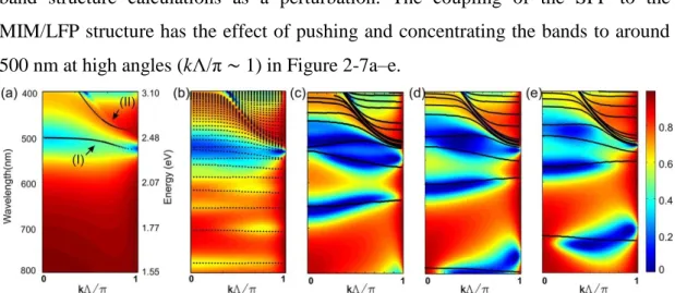
heavy atom, with a multiple localized states. (c) In a one-dimensional periodic arrangement of the light atoms, coupling through the surface plasmon mode can introduce a coupling of the LFPs and propagating bands can be formed. (d) Similarly, in a one-dimensional periodic arrangement of the MIM structures with a relatively thick top metal and a thin gap dielectric, the MIM modes and the LFP mode formed between consecutive MIMs are hybridized to form a diatomic molecule. The molecules are coupled to form the band structure of the diatomic crystal. (e) Effect of mode coupling is observed in the reflection coefficient, plotted as a function of wavelength and dielectric thickness, h, for a one-dimensional crystal. Numerical computation results are shown for a 250 nm period structure with 180 nm MIM width, for normal incidence. Resonance wavelengths are calculated using the Fabry–Perot resonator model for the MIM structures (black lines; see text for details) that are superimposed. Antisymmetric modes (even mode number m) are not coupled to the free-space modes at normal incidence and, therefore, contribute no absorption (arrow (i)). The LFP mode wavelength is estimated using the LC model (vertical line around 520 nm, denoted by arrow (ii)). (f) Reflection coefficient is plotted as a function of wavelength and dielectric thickness h at a 10° angle of incidence. Due to the broken symmetry, even modes also contribute to absorption. (g) Lumped circuit model for the diatomic unit cell consists of a transmission line capacitively coupled to a localized LC resonator representing the LFP mode. The model is used to calculate the resonance frequencies of the modes, plotted as dots, on top of the computational results in (f). The model captures the essential features of numerical calculations such as the resonance frequencies and anticrossing behavior due to coupling of modes. ... 19 Figure 2-7. (a) Band structure of a monatomic meta-surface is calculated using the circuit model in Figure 2g and the ABCD matrix approach and superimposed on the reflection obtained through numerical calculations. When the dielectric thickness is zero, only the bands formed are through coupling of the LFP (arrow I) modes via the surface plasmon mode (arrow II) are observed. (b) Increasing the gap to 3 nm results in the appearance of a large number of MIM modes and formation of a diatomic meta-surface. (c) Increasing the gap to 13 nm results in a reduction of the number of MIM modes, while increasing the absorption in the coupled bands due to improved
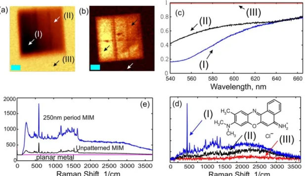
structures are shown in (d) and (e) for 180 and 160 nm MIM widths, with 250 nm period. Color bar shows corresponding reflectance values. ... 20 Figure 2-8. Theoretical and experimental reflectance plotted as a function of wavelength at normal incidence for (a) one-dimensional, 250 nm period structures with nanowire widths of 180 nm (I), 170 nm (II), 160 nm (III), 150 nm (IV), 140 nm (V) and (b) one-dimensional, 300 nm period structures with nanowire widths of 200 nm (I), 190 nm (II), 180 nm (III), 170 nm (IV), 160 nm (V). (c) TM mode reflectance for a 10 nm band around 550 nm observed with different numerical apertures (20×, 50×, and 100× objectives) on one-dimensional 250 nm period 150 nm width structures. Insensitivity to numerical aperture demonstrates the quasi-omni-directional absorption of the surfaces. ... 21 Figure 2-9. (a) Reflectance map (540–600 nm band) acquired using a 20× objective (NA 0.4) on a 250 nm period structure with 200 nm MIM width. (b) Raman spectra map (intensity of 591 cm–1 band, collected with 100 μW excitation power at 532 nm, 20× objective, 100 ms dwell time per pixel) of Cresyl Violet monolayer on the same structure. Scale bar is 10 μm. (c) Reflectance as a function of wavelength for several locations and (d) corresponding Raman spectra. Reflectance is plotted at two different locations (I) and (II) as referenced to location (III). Due to non-uniformity of the fabrication process, a gradient of the resonance wavelength is observed from top-right position to bottom-left position. When the absorption overlaps with excitation and emission wavelengths, improved Raman scattering is observed. Inset shows chemical structure of Cresyl Violet. (e) Raman signal is collected using a longer integration time (22 s, 100 μW excitation power) on a planar silver surface, unpatterned MIM, and 250 nm period MIM regions. Although Cresyl Violet exhibits no Raman signal on the plane metal surface, some enhancement is seen on unpatterned MIM regions, possibly due to the surface roughness of the top layer. .. 23 Figure 2-10. (a) Superimposed Raman spectra collected from 1600 individual spots over an area of 10 μm × 10 μm (100 μW excitation power, 100× objective, and 40 ms dwell time per pixel). (b) Histograms of intensity of two spectral locations shown by arrows (I) and (II) demonstrate uniform signal intensity within ca. 10% of average value for the fluorescence (arrow II) and ca. 20% for the Raman signal (arrow I). (c) Raman map formed using the 591 cm–1 Raman band (scale bar 2 μm) where the contrast is enhanced to show several dead-spots with submicrometer dimensions, demonstrating the high-resolution imaging capability with such substrates. ... 24
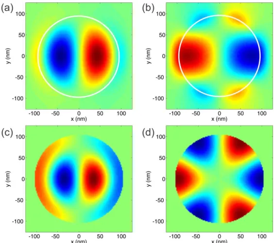
Figure 2-11. (a) Enhancement factors (EF) averaged over various regions (see inset in c) for a MIM structure with 50 nm periodicity, 10 nm top metal thickness, 20 nm dielectric gap, and 30 nm top metal width. (b) Maximum value of EF for different regions for the geometry in panel a. (c) Average EF values for a MIM structure with 100 nm periodicity, 20 nm top metal thickness, 20 nm dielectric gap, and 80 nm top metal width. (d) Maximum value of EF for different regions for the geometry in panel c. (e) Average EF values for a MIM structure with 250 nm periodicity, 50 nm top metal thickness, 20 nm dielectric gap, and 230 nm top metal width. (f) Maximum value of EF for different regions for the geometry in panel e. It is seen that shrinking the MIM size results in fewer resonances and improved average enhancement over the unit cell, especially on the top surface (10 nm thick slab over the top metal). The maximum values of the EFs are much higher than the average, showing the inherent spatial non-uniformity of enhancement. Comparing panels a–c, it is seen that tuning of the resonances through choice of geometry greatly improves EF for the wavelength range of interest (532 to 650 nm). ... 26 Figure 2-12. Sem images of polarization independent plasmonic metamaterial surface. The fabricated structures are dis-shaped despite they are aimed perfect squares. ... 28 Figure 2-13. (a) Schematic description of the proposed MMA structures. Top (b) and side (c) view of simulated structures. Periods in x and y directions are 250nm. W is width of the patches and R is the curvature of the corners. ... 29 Figure 2-14. (a) Absorption spectra of the MMA structure with perfect nano-square patches (R=0nm) for tox= 0 (blue) and tox= 30nm (green) (b) Absorption spectra for various nano-square patch widths (tox= 30 nm). Magnetic (c) and Electric (d) field profiles at the resonances shown in (a). ... 31 Figure 2-15. Effect of the curvature on the absorption spectra for W=200nm (a,b) and W=210nm (c,d) for tox=30nm. Effect of the oxide thickness on the absorption spectra for W=200nm and R=100nm (e-f). The magnetic plasmon mode splits into two modes at smaller radius as the width of the resonator increases. ... 32 Figure 2-16. Origin of resonances for W=200nm, R=100nm and tox=30nm. Simulated z component of electric field profiles for λ=550nm (a) and λ=600nm (b). Calculated electrical field profiles for modes m=1, n=2 (c) and m=3, n=1 (d). ... 33
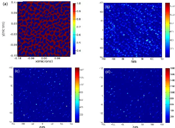
Figure 2-17. Effect of side angle on the absorption spectra. (a) Cross section of the simulated structure. (b-c) Absorption spectra with respect to the side angle. As the slope of the cone increases absorption of magnetic resonance mode decreases. ... 34 Figure 3-1. (a) Scanning Electron Micrographs (SEM) of plasmonic surfaces with 1, 3 and 5 nm mass thickness Ag overlayer shows coarsening and percolation of Ag nanoislands. Scale bars 250 nm. Plasmonic field enhancement is greater as the nanoislands approach each other, reducing the inter-particle gap. 3 nm mass thickness sample exhibits greatest hot spot density. (b) Schematic view of the substrate showing layer structure. (c) Reflectance of the surfaces near normal incidence for 1, 3 and 5 nm mass thickness Ag over-layer and 30 nm HfO2. Gray band shows the wavelength region of interest for Raman scattering excited by 532 nm light. Ag mass thickness of 3 nm results in a wide band meta-surface. (d) The reflectance is plotted for HfO2 thicknesses of 5, 10, 20 and 30 nm. (e) Dependence of reflectance on angle of incidence is plotted for 20, 30, 40, 50, 60, 70 and 80 degrees. The 30 nm HfO2/ 3nm Ag surface is quasi-omni-directional, maintaining high absorption over a wide wavelength range at angles up to 60 degrees. ... 37 Figure 3-2. . (a) Maximum |E|2 field enhancement factor as a function of wavelength, plotted for 10, 20 and 30 nm dielectric thickness for a periodic arrangement of Ag nanoislands (40 nm period, 10 nm thickness, 35 nm island size, 75 degree sidewall angle), shows increase in the enhancement around 550 nm as thickness increases to 30 nm. (b) Calculated reflectance of the periodic arrangement, plotted as a function of wavelength. (c) Maximum |E|2 field enhancement factor as a function of wavelength, for a quasi-random surface derived from SEM data as a function of dielectric thickness. (d) Calculated reflectance of the quasi-random arrangement, plotted as a function of wavelength and dielectric thickness. A dielectric thickness of 40 nm is also included in the calculations, as it better fits the experimental reflectance for 30 nm HfO2 shown in Figure 3-3. ... 38 Figure 3-3. SEM derived surface model for field enhancement and reflectance calculations. a) The SEM data is used to extract silver island shapes. b) Field enhancement factor (|E|2 for 550 nm excitation) at the top metal-dielectric interface. c) Field enhancement in the middle point of upper boundary of the top metal and dielectric interface. d) Field enhancement at the upper boundary of the metal islands ... 39
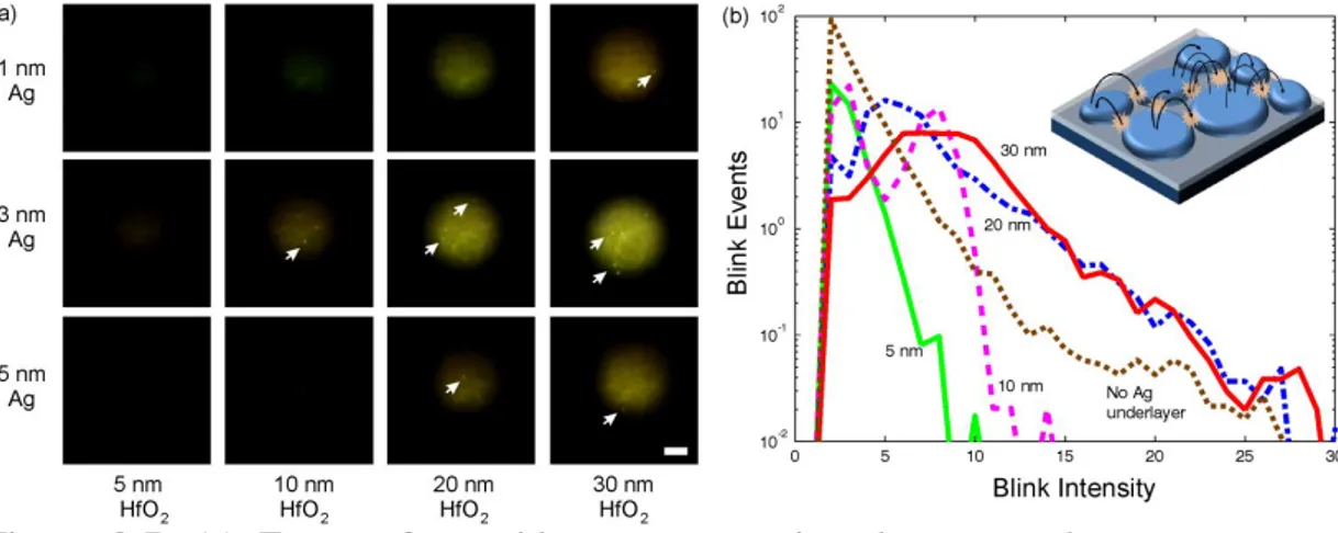
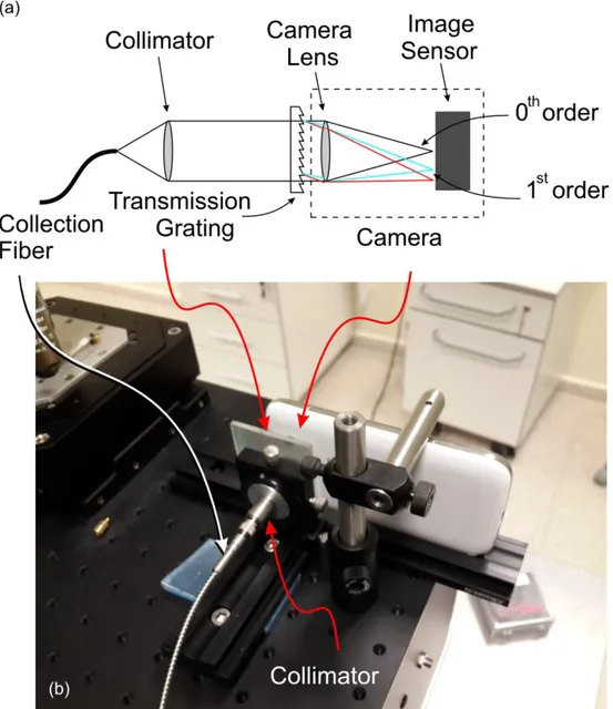
Figure 3-4. (a) Cross sectional magnetic field profile for a periodic arrangement of metal-insulator-metal resonators (40 nm period, 35 nm width, 20 nm thickness, 75 degree sidewall angle Ag, on 20 nm HfO2, on Ag) at 430 nm excitation wavelength and (b) at 700 nm excitation wavelength. (c) For a top metal thickness of 10 nm, fields have enhancement at the top surface (excited at 550 nm) as compared to (d) a top metal thickness of 20 nm (all scale bars are 20 nm wide). ... 39 Figure 3-5. (a) Time series of the integrated intensity within 0 to 3500 cm-1, as recorded by the cooled CCD spectrometer on a particularly bright hot-spot, shows blinking events as fluctuations in the intensity (500 µW of excitation at 532 nm). (b) The time series plotted to feature the full spectrum exhibits Raman lines that fluctuate in intensity and frequency, characteristic of single molecule SERS. (c) Occasionally, a fluorescent molecule is captured in the hot-spot (at time 35 s in (a)). (d) Typical Raman spectra during a SERS blink (at time 76 s in (a)) exhibits a broad fluorescence superimposed with distinct Raman bands. ... 42 Figure 3-6. a) Schematic of the measurement set-up for using the camera of a smart-phone for imaging with a confocal Raman system. b) Photograph of the measurement set-up showing various components described in (a). ... 43 Figure 3-7. (a) Frames from video captures using the smart phone camera on plasmonic surfaces with 1, 3 and 5 nm mass thickness Ag over-layer and 5, 10, 20, 30 nm HfO2 dielectric layer thickness. Excitation laser is defocused to illuminate an area 50 µm in diameter. Arrows denote blink events on a fluorescence background of the Ag nano-island layer. Scale bar is 20 µm wide. (b) Video frames are analysed to extract a histogram of blink event intensity for the 3 nm Ag samples at varying HfO2 thickness. A dielectric thickness of 30 nm produces brightest blink events. As the bottom Ag layer is removed (dielectric thickness infinite), blink events can still be observed, however at a decreased rate and intensity. Inset shows the potential source of blinking, i.e. surface diffusion of physisorbed volatile organic compounds into and out of hot-spots. ... 43 Figure 3-8. a) Schematic of the spectrometer configuration. b) Photograph of the measurement set-up showing various components described in (a). ... 44 Figure 3-9. (a) Configuration for using the smart phone camera as a low resolution spectrometer. The collection fiber from the Raman set-up is collimated and dispersed
excitation using the cooled CCD spectrometer are shown. (c) Smart phone camera recordings of the two orders of the dispersed input light in the snap-shot mode. Solid blue lines show integrated pixel intensity and dotted red line shows superimposed Raman spectra convolved with a lineshape function that represents the point spread function (PSF) of the optical configuration. Insets show actual camera excerpts. (d) Close-up of the second order diffraction region of the camera output (solid lines) superimposed with Raman spectra shown in (b) convolved with the PSF of the configuration. ... 46 Figure 3-10. (a) False color coded excerpts from series of smart phone camera snapshot captures during blink events on the plasmonic substrate, in the spectrometer configuration (1 mW excitation at 532 nm). The spectral region is cropped, rotated and stitched for each frame. Inset shows actual camera color coding of the same data. Integration time per frame is ~ 1 sec. (b) False color coded excerpts from a video sequence recorded at 30 frames per second. Although video recording is at lower resolution, distinct spectral features during blink events can be observed (also see Supporting Video). The SERS spectra of plasmonic surfaces (30 nm HfO2 thickness) were also recorded using the cooled CCD spectrometer, treated with 10 nM Methylene Blue solution in (c) and 1 µM Cresyl Violet solution in (d) using 100 µW excitation. Corresponding spectra are also captured using the smart phone camera as shown in (e) and (f). Insets show excerpts of the region of interest from actual camera captures in snapshot mode. ... 47 Figure 3-11. (a) Cross-section of the MIM surface during an XPS measurement with laser illumination. Jx represents the X-ray induced photoemission current into the vacuum. (b) The band diagram of the MIM junction under X-ray and laser illumination. Hot-electron energy distributions are shown with rectangles above the Fermi level, due to absorption of light in the top and bottom metal layers. (c) A simplified circuit model with various currents acting on the top metal layer which acquires a steady state voltage of Vs. Current JT through the dielectric is modeled within a first order approximation by the resistor RT. ... 49 Figure 3-12. (a) Schematic description of the MIM grating structures used in polarization dependent measurements. (b) Calculated field profiles of the structures for TE and TM polarizations. Field enhancement is minimal for TE polarization, while plasmonic enhancement is present in the gap for TM polarization. (Scale bar 50 nm). (c) XPS spectra of the Ag 3d peaks acquired on gratings labeled as (I) and
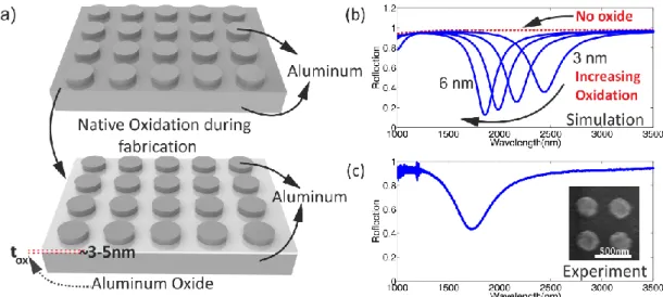
(II) for two polarizer orientations. As the polarizer is rotated from 0° to 90°, apparent binding energy shifts of the Ag 3d3/2 and 3d5/2 are observed for the gratings with different orientations. Each polarization excites only one of the gratings, for which the plasmonic modes are excited... 50 Figure 3-13. (a) Scanning electron micrograph of MIM surface fabricated by atomic layer deposition of HfO2 on Ag and self-organized formation of Ag nanoislands on HfO2 upon 3 nm thick Ag evaporation (Scale bar 250 nm). (b) Reflectance of the surfaces for incidence angles ranging from 20° to 80° shows a broad plasmonic absorption peak around 580 nm. (c) Photo-response of the MIM surface when illuminated by 532 nm excitation, measured by XPS. (d) Consecutive measurements of the XPS spectrum under dark and illuminated conditions exhibit repeatable differential shifts of the Ag 3d lines. (e)–(h) Same as in (a)–(d) except the top Ag mass thickness is 5 nm and a semicontinuous Ag film is formed instead of MIM nano-islands and no surface photovoltage is observed. ... 52 Figure 3-14. a) XPS spectra of the Ag 3d peaks measured on the MIM surface for dark and illuminated conditions, using lasers of 650, 532, and 445 nm wavelength, 20 mW power. The binding energies shift to negative due to hot-electron tunneling from the bottom metal to the top Ag island. Greater shifts are observed for increasing photon energy. (b) As the illumination intensity (445 nm) is increased from 5 to 20 mW, greater negative shift of the binding energy is observed which saturates at high intensities. ... 53 Figure 4-1. (i) Thermal evaporation of Al on silicon substrates. 3nm germanium is evaporated as an adhesion layer prior to Al deposition. (ii) Formation of a thin aluminum oxide (Al2O3) layer upon exposing the Al films to air for e-beam lithography. (iii) ~100nm PMMA is spin coated and annealed at 180˚C for 120 seconds. (iv) Patterns are formed using e-beam lithography. (v) 50nm of Al or Ag is evaporated. (vi) Lift-off process to form the final structures. ... 60 Figure 4-2. Verification of NO-MIM structures through observations of resonances in NIR. (a) Schematic of formation of NO-MIM surfaces during fabrication process (Top patterned layer height is 50 nm). (b) Simulated reflectance spectrum of NO-MIM structures for various Al2O3 thicknesses. While no plasmonic resonance is observed in the absence of native oxide, plasmonic resonances in NIR are observed
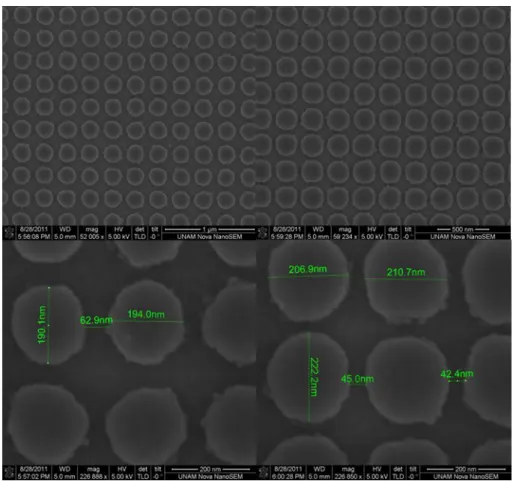
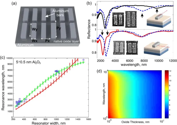
Diameter and period of the discs are 250nm and 400nm, respectively. (Inset) SEM image of the nanodisc array. ... 60 Figure 4-3. Characterization of the native oxide thickness over a time span of 24 days using XPS. (a) XPS spectrum of an aluminum film. High energy shoulder corresponds to the aluminum oxide peak. (b) Evolution of the calculated native oxide thicknesses. ... 61 Figure 4-4. Resonance tuning in the NIR and MIR range using anisotropic Al bar arrays. (a) Schematic of asymmetric NO-MIM structures with nonidentical periods and widths along x and y directions to excite multiple modes in IR (Top patterned layer height is 50 nm). (b) Typical reflection spectra showing multiple resonances in the NIR and MIR range due to the asymmetry of the structures with Px=500nm, Py=2000nm and Wx=310nm and Wy=1000nm (black curve), 1500nm (blue curve) (top) and Wx=250nm (red curve), 310nm (blue curve) for Wy=1000nm (bottom). (Inset) SEM images of corresponding structures. Red dashed lines on the cartoon illustrations indicate the axis on which the structures’ width is modified. (c) Experimentally observed resonance wavelengths as functions of the Al bar width either along the short or long axis (blue dots). Calculated resonances by treating the NO-MIM structures as Fabry-Perot (FP) resonators consisting of truncated waveguides (green and red curves). A better fit of the FP resonator model to the experiments can be achieved if the dielectric function of Al2O3 is assumed to be wavelength dependent (green curve), as opposed to a constant (red curve, n=1.6). Vertical lines on the curves are errors bars corresponding to 0.5nm uncertainty in the oxide thickness. (d) Effective refractive index of the waveguide forming the FP resonator as a function of Al2O3 thickness, using the wavelength dependent dielectric function. ... 63 Figure 4-5. Simultaneous resonances in visible and NIR regime using 1D NO-MIM. (a) Schematic of 1D NO-MIM structures. tgr=50nm and P=250nm. Experimental results showing tuning of resonance wavelengths as W changes between 110 and 150nm, (b) in the visible and (c) in the NIR regime. Simulation results for the experimented structures shown in (d-e) being in a good agreement with the experimental results. Each spectrum curve is shifted by 1 along y-axis for clarity. (f) First order (m=1) and third order (m=3) mode profiles corresponding to NIR (ii) and visible (i) resonances as indicated with arrows in (d) and (e). The even mode (m=2)
is not observed for normal incidence. In the simulations 5nm of native oxide layer thickness is assumed. ... 64 Figure 4-6. SEM images of Ag nanoparticles on silicon and their size distribution. 65 Figure 4-7. Nano-particle based large area NO-MIM structures. (a) Reflection spectra for Ag nano-particle based NO-MIM structures. Resonance blue-shifts if the time period between two deposition processes increases (dashed and solid red lines). No resonance is observed if the deposition of Al and Ag is done without breaking the vacuum (blue solid line). (Inset) SEM images of 3nm Ag on Si(i) and Al(ii). (c) Simulation results and simulated structure (inset) for tox=3nm and 5nm. Simulated structure is a periodic array of truncated cones with D=35nm, P=40nm, tgr=20nm and θ=75 degrees ... 66 Figure 4-8. SEIRA on NO-MIM structures with patterned Ag top layer fabricated by e-beam lithography. Reflection spectra of these structures before (blue) and after (green) DDT monolayer formation for (a) Wx,y=300nm and (b) Wx,y=350nm. Periods along x and y directions are the same (Px=Py=50nm). (c) and (d) First derivative of the reflection spectra in (a) and (b), respectively. Molecular signatures of PMMA and DDT are more visible in the first derivative curves in (c) and (d) compared to the reflection spectra in (a) and (b). (e) An SEM image of the fabricated structures. (Scale bar: 1 μm ). ... 68 Figure 4-9. (a) Infrared reflection spectrum of the monolayer DDT on bare Ag mirror measured under Grazing Angle Illumination after background subtraction. (b) Infrared reflection of the monolayer DDT on the NO-MIM structures with Ag top layer after background subtraction. ... 69 Figure 4-10. SEIRA detection of molecular monolayers on hierarchical NO-MIM structures. (a) Schematic of hierarchical NO-MIM structures before and after nanoparticle deposition with top patterned layer height of 50 nm. Periods and widths along x and y directions are the same, Px=Py=500nm and Wx=Wy=350nm. (b) SEM image of NO-MIM structures after 3nm Ag deposition (Scale bar: 500nm). (c) FTIR reflection spectrum of thick DDT solution on a bare Al film. Region of interest is highlighted in grey. (Inset) Molecular sketch of DDT molecule. (d) FTIR reflection spectra of NO-MIM structures for: (i) just after fabrication of all Al NO-MIM structures, (ii) after plasma cleaning of PMMA residues, (iii) after the formation of
between 2500 and 3500 cm-1, and its derivative (f) for better visualization of stretching of monolayer DDT molecules. Arrows mark the DDT and PMMA signatures in (e). Molecular signatures (2930 cm-1 and 2955 cm-1) of PMMA are observable before oxygen plasma cleaning. No distinctive bands are observed after oxygen plasma (ii) and Ag deposition (iii). ... 70 Figure 4-11. (i) Thermal evaporation of Al on silicon substrates. 3nm germanium is evaporated as an adhesion layer prior to Al deposition. (ii) Formation of a thin aluminum oxide (Al2O3) layer upon exposing the Al films to air for e-beam lithography. (iii) ~100nm PMMA is spin coated and annealed at 180˚C for 120 seconds. (iv) Patterns are formed using e-beam lithography. (v) 50nm of Al is evaporated. (vi) Lift-off process to form all Al MIM structures. (vii) O2 plasma cleaning for PMMA residue removal and formation of a thin oxide film on the top Al structures. (viii) Formation of Ag nanoparticles through evaporation of 3nm Ag film. ... 71 Figure 4-12. (a) Reflectance spectra for Ag nanoparticles-based NO-MIM (blue), all Al NO-MIM (red) and hierarchical NO-MIM (green) surfaces in the visible regime. (b) Reflectance spectra for all Al NO-MIM and hierarchical NO-MIM (red) surfaces in the MIR regime. ... 72 Figure 4-13. Characterization of NO-MIM structures fabricated using Focused Ion Beam (FIB) milling. (a) Fabrication steps for NOMIM structures: (i) Thermal evaporation of 100nm of Al on silicon substrates, (ii) formation of a thin aluminum oxide (Al2O3) layer upon exposing the Al films to air, (iii) thermal evaporation of 50nm of Ag, (iv) FIB patterning of the top Ag layer. (b) Measured (100μmx 100μm) area with respect to the fabricated area (50μmx 50μm). (c) Top-view and cross-section (inset) SEM images of FIB fabricated surfaces. (d) Reflectance spectra for the FIB fabricated surfaces with shown widths and periods. ... 73 Figure 4-14. SERS detection of molecular monolayers on hierarchical NO-MIM structures. (a) Raman Spectra of a thick DDT solution on 80nm Al coated silicon. (b) SERS spectra of monolayer DDT on hierarchical NOMIM surfaces and an Al coated Si substrate. Integration time and laser power are 100ms and 0.5mW, respectively, for hierarchical NOMIM surfaces; where they are 10s and 13mW, for Al films on Si. (c) Simulated field profiles for all Al MIM (MIM1), Ag nano-particle based NO-MIM (NO-MIM2) and hierarchical NO-NO-MIM (NO-MIMIM) structures. (d) Optical micrograph of hierarchical NO-MIM surfaces. (e) SERS mapping of DDT on
hierarchical NO-MIM surfaces. Brighter and darker regions emphasize hierarchical NO-MIM and nano-particle based NO-MIM structures, respectively. (f) Wide-field CMOS camera image of blink events on NO-MIM structures. Blink events are only observed on hierarchical NO-MIM structures. ... 75 Figure 4-15. (a) 3D and (b) side view of the hierarchical aluminum surfaces. Top Al layer thicknesses (tgr1 and tgr2) are 50nm. The thicknesses of the bottom and top oxide layers are denoted as tox1 and tox2, respectively. (c) Top-down SEM image of the fabricated structures. (d) Fabrication of hierarchical Al structures. (i) Deposition of 80 nm thick Al. (ii) Formation of native Al2O3 after exposure of the Al films to air. (iii) PMMA coating. (iv) Pattering PMMA with e-beam lithography. (v) Deposition of the 1st 50 nm thick Al. (vi) Formation of the 2nd native Al2O3 layer after vacuum break. (vii) Deposition of the 2nd 50 nm thick Al layer. (viii) Lift-off process. ... 77 Figure 4-16. Depth dependent XPS characterization of Al surfaces with thin native Al2O3 on top. (a) Just after the deposition of Al films. (b) After the fabrication of hierarchical Al structures. ... 78 Figure 4-17. (a) Measured and (b) simulated reflectance spectra for W=290nm, 300nm, 320nm and 340nm (Period=500nm). (c) Magnetic field intensities for the resonances shown in (b). ... 79 Figure 4-18. Simulated reflection spectra for the hierarchical MIM structure with two oxide layers assuming different extinction coefficients for the native oxide layer.... 80 Figure 4-19. Simulated reflection spectra for (a) varying tox-1 and tox-2, (b) varying t ox-2 with tox-1=5nm. W=300 nm, P=500 nm for all cases ... 81 Figure 4-20. (a) 3D schematics of higher order hierarchical aluminum surfaces with multiple MIM resonators. Simulated reflectance spectra for structures with (b) 3, (c) 4 oxide layers. (d) Corresponding magnetic field profiles for the resonances shown in (c). The thickness of the top Al layers is 50nm, W=300nm and P=500nm for both geometries. ... 82 Figure 5-1. Sensing performance of various optical platforms. 5 nm PMMA (a) suspended in air, (b) on semi-continuous CaF2 substrate, (c) on 300 nm a-Si/Al surface, (d) on 400 nm a-Si/Al surface. (i) Simulated electric field enhancement profiles on cartoon illustrations at λ: 5780 nm (1/λ: 1732 cm-1). (ii) Simulated electric field enhancement factors on the surface of each structure, (iii) far-field signal
Measured optical properties of PECVD deposited a-Si are used for the simulations (n: 3.3 in the IR, see Figure S11). Optical properties of PMMA are fitted to a Lorentzian oscillator (Figure S12) centered around 5780 nm. ... 87
List of Tables
Chapter 1
Introduction
Surface plasmons are known as propagating electromagnetic waves at metal-dielectric interfaces. The field of plasmonics deals with interaction of electromagnetic waves with metal surfaces and nanostructures. Since, the surface plasmon field is tightly confined to the interface; electromagnetic field intensity is enhanced at the metal-dielectric interface. Various optical sensors[1]–[3], interconnects[4]–[7], photodetectors[8]–[11], optical elements[12] and photovoltaic devices[13], [14] utilize such unique characteristic of surface plasmons. There are different ways of exciting surface plasmons at metal-dielectric interfaces such as electrons and light[15]–[17]. Among the excitation sources, light is the most common and easiest way of exciting surface plasmons[18].
Metallic nanoparticles, on the other hand, provide an easier route for plasmonics research due to ease of fabrication and characterization methods[15], [19], [20]. Various fabrication methods are utilized plasmonic metallic nanoparticles. E-beam lithography[21], [22], focused ion-beam lithography[23], nano-imprint lithography[24], [25], interference lithography[26] and nano-sphere lithography[27], [28] are among the top-down fabrication methods where nanoparticles with uniform size distributions can be fabricated. Despite the uniformity and resolution of fabricated devices, top-down fabrication methods like e-beam lithography and focused-ion-beam lithography suffer from high fabrication costs and small fabrication areas. Periodic nanopatterns can be fabricated over large areas using interference lithography and nanosphere lithography, even at wafer-scale[1], [26]. Physical vapor deposition (PVD) of nanoparticles on the other hand emerges as one of the easiest way of fabricating nanoparticles over large areas without using
chemical processes[29], [30]. Thermal evaporation and e-beam evaporation are among the most used PVD methods to fabricate metal nanoparticles[29], [31]. However, the control of physical vapor deposition of nanoparticles lacks order and uniformity due to stochastic nature of nanoparticle formation process[32], [33]. Dewetting of metal films results in nanoparticles during PVD process due to the surface energy difference between the substrate and metal film. Depending on the substrate, the thickness of the metal film, the size of nanoparticles and the interparticle distance change. The size of nanoparticles also differs depending on the deposition rate and the thickness of the metal[30]. Moreover, the post-fabrication processing of metal nanoparticles such as thermal and laser annealing modify the final shape and the interparticle distance of nanoparticles[34], [35]. On the other hand, fabrication of nanoparticles by chemical means gives flexibility to fabricate nanoparticles in low-costs with large amounts with fair size distributions[36]. Nanoparticles can be fabricated in various shapes which further provide different functionalities for specific applications[20].
When nanoparticles are brought together, they start interacting optically[37], [38]. The interaction between nanoparticles can be intuitively understood as the coupling of individual resonators which results a shifted energy spectrum compared to the individual resonators' energies[39]. Due to coupling, plasmonic coupled systems offer a very rich energy spectrum[40], [41]. Since, energy spectrums of coupled structures are broad or multispectral they are desired for various nanophotonics and plasmonic applications. Coupled plasmonic structures are fabricated by either top-down or chemical methods[19], [42]. The aggregating nanoparticles in solutions results another plasmon peak in the red wavelengths which is due coupling of nanoparticles[43]. Scattering spectra of nanoparticles changes drastically when they get close to metallic planes due to hybridization of surface plasmon and localized plasmon modes and resulting gap plasmon modes in between[44]. Gap plasmon modes are also known as metal-insulator-metal (MIM) modes when they are excited between two metal planes. MIM geometry offers rich physics as well as plasmon enhanced applications rooted in classical and quantum electromagnetics[45], [46]. Negative index metamaterials, superlensing, metamaterial absorbers, color printing, photodetectors, plasmonic sensors and surface enhanced spectroscopies are few of
One of the applications of plasmonic surfaces studied here is label-free sensing. Labeled sensing platforms are tagged with fluorescent molecules or quantum dots which are prone to bleaching or deterioration[55], [56]. Label-free sensing strategies are developed to overcome the difficulties that labeled sensing platforms face. Surface plasmon sensors (SPR) are the known as the golden standard for the label-free sensing platforms. Bulk prism based SPR systems are among the widely used plasmonic sensing platforms to probe bio-molecular binding events. Various sensing platforms have been developed on nanoparticles, gratings and plasmonic metamaterials utilizing top-down and bottom-up fabrication methods. Spectroscopic methods combined with plasmonic structures offer another route for label-free sensing methods. Surface enhanced Raman spectroscopy (SERS) provides vibrational information and molecular signatures of molecular moieties[57]–[59]. Typically, Raman spectroscopy requires large amount of molecules to probe molecules due to low probability of release of a Raman scattered photon. When, a monochromatic light (typically laser light) interacts with molecules' vibrational modes, scattered photons have either higher energy (Anti-Stokes) or lower energy (Stokes) than the excitation source. Anti-stokes signals are generally filtered out from the Raman spectra due to their low intensities. Since Raman signal scales with 𝐸 = |𝐸0|4, enhancing electromagnetic field intensity near the probe molecules increases the Raman signal enormously. In SERS enhancing electromagnetic field intensity by utilizing nanostructured metal surfaces enhances the Raman signal 4-10 orders of magnitude, thus enabling the possibility of detecting single molecules. On the other hand, debate on the origin of single molecule Raman events is still unresolved. The charge transfer between the metal and molecules might lead to the single molecule Raman events. This mechanism is also known as chemical enhancement factor. SERS platforms should provide electromagnetic field enhancement at the excitation and Stoke's wavelengths. Double resonant nanoantennas, metamaterials and plasmonic gratings are good examples for good SERS platforms where each resonance is accompanied with field enhancement[25], [60], [61]. Broadband plasmonic surfaces are desired as SERS substrates whose resonances span all the vibrational bands of a molecule.
Infrared absorption spectroscopy is a well established label-free tool used in biological and chemical sciences to identify molecular moieties by utilizing specific molecular vibrational bands in the infrared wavelengths[62]. Since the selection rules
in IR and Raman spectroscopy are different, the vibrational information of these techniques is complementary[63]. However, the absorption efficiencies of molecules for specific bands are low in the IR which limits the use of IR spectroscopy for small amount of molecules, molecular or protein monolayers. Different techniques are developed in the IR to identify molecules in small amounts. Attenuated total reflectance (ATR), infrared reflection absorption spectroscopy (IR-RAS) are two widely used tools to identify molecules[64], [65]. In ATR, electromagnetic field decays exponentially when light is sent through a high index prism to a low index medium. The enhanced field at the prism medium interface is used to increase absorption of molecules. Similar to ATR, electromagnetic field is enhanced when a p-polarized light is sent to a substrate at oblique incidences on which molecules are deposited. Metal nanoparticles and deterministically designed plasmonic metal nanostructures emerge as an alternative tool to detect minute amount of molecules[58], [66], [67]. The electromagnetic field is highly enhanced and concentrated around nanoparticles which results in the enhancement of the absorption of the molecules in close proximity. The absorption of the molecules is sensed in the far field signal (reflection/transmission spectrum). This powerful technique is also known as surface enhanced infrared absorption spectroscopy (SEIRA). However, there are some limitations to SEIRA. Vibrational bands of molecules are embedded in plasmonic resonance background in the farfield reflection spectra and data post processing is required to extract positions of vibrational bands. All of the vibrational bands cannot be detected because the electromagnetic field cannot be enhanced over very large bandwidths (3-20μm band) using single resonant plasmonic structures. Moreover, the positions and shapes of vibrational modes are modified due to strong coupling between plasmonic resonances and vibrational modes. Although electromagnetic field enhancement is on the order of 103-105 signal intensities suffer from low vibrational intensities (~1-5%). Therefore, field enhancements with high mode volumes are preferred over highly localized field enhancements.
Energy harvesting is another application area that plasmonics studies target. Plasmon enhanced photovoltaics is emerged as alternative to current solar cell technologies by either incorporating metallic nanophotonics structures to thin films
and increasing the absorption in semiconductor films to decrease the costs and thicknesses. Despite the huge amount of literature, the success of plasmons in photovoltaics area is debatable[72]. Still, the plasmonics promise a bright future for silicon photonics industry for the IR regime[8]. Structuring Schottky contacts with plasmonic structures enabled to use of silicon in photodetectors in the IR wavelengths with lower energy than silicon bandgap. Generation and capture of hot-electrons are the main mechanism for photodetection in these devices. In a Schottky diode, due to band alignment between metal and semiconductor layer, there is a band offset that is smaller than the band gap of the semiconductor. When light is absorbed by the metal contact, electrons are generated, which are either thermalizes or contribute to current through tunneling or hopping above the barrier. The electrons that have energy higher than the band offset are called hot-electrons. However, due to reflective nature of metals the most of the incident light is reflected, thus the generation rate of hot electrons is small. By patterning Schottky contacts, hot-electron generation can be increased due to plasmon enhanced electromagnetic field[8], [14]. MIM resonators emerge as one of the novel hot electron photodetection devices[52], [73]. Similar to Schottky based hot-electron devices, by patterning the metal contacts plasmons are employed to increase hot-electron generation rate. Since these devices utilize high bandgap insulators between two metal contacts, the photoresponsivities are small compared to Schottky based hot electron devices.
Perfect absorption of light is important for aforementioned and can be obtained using patterned metallic surfaces through exciting plasmons. On the other hand, strong interference coatings offer an easier way for perfect light absorption by using ultrathin absorbing semiconducting films[74], [75]. When a thin dielectric film is deposited on a metal surface, resonant light absorption occurs at thicknesses; 𝑡 ≅ λ/4n, where n is the dielectric constant and λ is the resonance wavelength. If the dielectric constant increases the resonance thickness becomes 𝑡 < λ/4n due to increased nontrivial phase at metal dielectric interface. If the dielectric film has a non-zero extinction coefficient (𝑛 = 𝑛̃ + 𝑖𝑘̃), the thickness decreases to 𝑡 ≪ λ/4n and depending on the refractive index function of metal and dielectric resonance thickness changes. Non-zero extinction coefficient results small phase accumulation at oblique angles and the absorption becomes wide-angle. Since these types of coatings exhibit distinct colors depending on the resonance wavelength, most of the
applications concentrate on reflective type color filters[74]–[78]. Light absorption on these coatings can be exploited as novel photodetectors.
In this thesis, we first develop a circuit model to understand the coupling mechanism of a coupled system based on MIM geometry. Our findings are supported with experimental results by fabricating and characterizing the proposed structures. These structures are utilized as SERS substrates with unity enhancement over large areas. Fabrication imperfections are exploited to achieve triple band plasmonic absorber geometry due to excitation of three different plasmon modes. Then, following theoretical and analytical study, MIM structures with nanoparticle top layer are fabricated. By optimizing the conditions for nanoparticle formation, large area, wide angle and broadband plasmonic surface are achieved. Single molecule Raman blinking events are observed with these structures using a confocal Raman microscope equipped with cooled CCD spectrometer. Single molecule Raman events are also detected when a mobile phone's camera used instead of cooled CCD spectrometer. To the best of our knowledge this is the first observation of a single molecule Raman blinking event using a cmos camera. Same surfaces are also used as a photodetector to probe hot electrons using a x-ray photoemission spectroscopy (XPS) system. The final part of plasmonic studies includes aluminum based plasmonic surfaces. By exploiting native oxide layer on Al forming during the fabrication processes, we are able to realize plasmonic surfaces in the visible and IR wavelengths. These surfaces are used as SERS and SEIRA platforms simultaneously. To address the issues of plasmonic surfaces such as low signal intensities narrow bandwidth, small surface area and costs, thin film interference coatings are proposed as novel sensing platforms in the infrared and visible wavelengths. These coatings perform better than conventional plasmonic surfaces when they are used as infrared sensing platforms. Similar surfaces are used as colorimetric sensor platforms to sense protein monolayers and bilayers.
Chapter 2
Well-Defined Coupled Plasmonic
Structures
Plasmonic metamaterials allow confinement of light to deep subwavelength dimensions, while allowing for the tailoring of dispersion and electromagnetic mode density to enhance specific photonic properties. Optical resonances of plasmonic molecules have been extensively investigated; however, benefits of strong coupling of dimers have been overlooked. In this part, a novel plasmonic geometry and its surface enhanced Raman spectroscopy application are demonstrated. Then, fabrication related issues are exploited for a multispectral metamaterial absorber. Before going into details of this chapter, surface plasmon at different metal dielectric interfaces are studied.
Parts of this chapter were published as;
1. Sencer Ayas, Hasan Guner, Burak Turker, Oner Ekiz, Faruk Dirisaglik ,Ali Kemal Okyay and Aykutlu Dana, "Raman Enhancement on a Broadband Meta-Surface", ACS Nano, 2012, 6 (8), pp 6852–6861
2. Sencer Ayas, Gokhan Bakan and Aykutlu Dana, "Rounding corners of nano-square patches for multispectral plasmonic metamaterials absorbers" Optics
2.1. Surface Plasmons at Metal-dielectric Interface
To understand the coupling conditions, a very simple geometry (metal-dielectric interface) is used to give the basics of surface plasmons [79]. We start with the assumption of evanescently decaying and propagating surface plasmons in the z and x-directions respectively as shown in Figure 2-1.
Figure 2-1 Surface plasmon excitation scheme at metal-dielectric interface. For a TM polarized wave, electric and magnetic fields are given as
𝐻𝑦(𝑧) = 𝐴𝑒𝑖𝛽𝑥𝑒−𝑘𝑑𝑧 (2.1) 𝐸𝑥(𝑧) = 𝑖
𝐴𝑘𝑑 𝜔𝜀𝑜𝜀𝑑
𝑒𝑖𝛽𝑥𝑒−𝑘𝑑𝑧 (2.2)
for z>0 (dielectric region)
𝐻𝑦(𝑧) = 𝐵𝑒𝑖𝛽𝑥𝑒𝑘𝑚𝑧 (2.3)
𝐸𝑥(𝑧) = −𝑖 𝐵𝑘𝑚 𝜔𝜀𝑜𝜀𝑚𝑒
𝑖𝛽𝑥𝑒𝑘𝑚𝑧 (2.4)
for z<0 (metal region).
By equating Hy and Ex at z=0 we obtain A=B and Akd/εd=-Bkm/ εm. Hence: 𝑘𝑚
𝜀𝑚= −
𝑘𝑑
𝜀𝑑 (2.5)
Since propagation constants and 𝜀𝑑 are real, surface plasmons are supported for materials at the metal-dielectric interface which have negative dielectric constants. Typically, metals have negative dielectric functions above plasma frequency. Although, plasma frequencies of metals are in the deep-UV regime, some metals have real dielectric functions in the visible portion of the spectrum due to interband
limits the use of Au in the UV wavelengths. Using βx2=ko2εd,m-(kd,m)2 and Equation 2.5 together results surface plasmon dispersion relation 𝛽𝑥 = 𝑘𝑜√
𝜀𝑑𝜀𝑚
𝜀𝑑+𝜀𝑚 . In a
similar manner, we can derive the surface plasmon coupling condition for TE polarized waves.
For a TE polarized wave electric and magnetic fields are given as
𝐸𝑦(𝑧) = 𝐴𝑒𝑖𝛽𝑥𝑒−𝑘𝑑𝑧 (2.6)
𝐻𝑥(𝑧) = 𝑖 𝐴𝑘𝑑
𝜔𝜇 𝑒
𝑖𝛽𝑥𝑒−𝑘𝑑𝑧 (2.7)
for z>0 (dielectric region)
𝐸𝑦(𝑧) = 𝐵𝑒𝑖𝛽𝑥𝑒𝑘𝑚𝑧 (2.8)
𝐻𝑥(𝑧) = −𝑖 𝐵𝑘𝑚
𝜔𝜇 𝑒
𝑖𝛽𝑥𝑒𝑘𝑚𝑧 (2.9)
for z<0 (metal region).
The continuity equation for Ey and Hx at the metal-dielectric interface (z=0)
results in A=B and Akd+ Bkm=0 where we obtain the relation A(kd+ km)=0. Since kd,m>0, A=0 is the only condition for TE mode. Thus, Ey=0, Hx=0and the surface
plasmons are not supported for TE polarized waves.
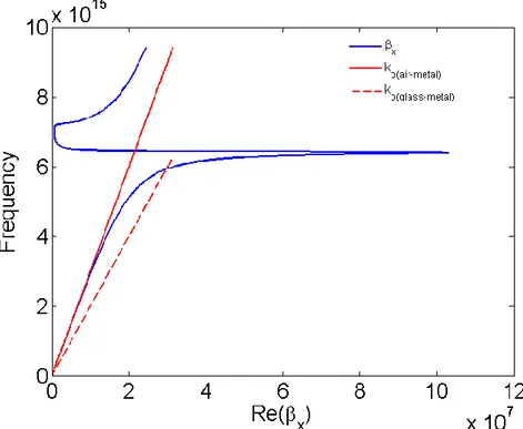
So far, a propagating wave at a metal-dielectric interface is assumed to derive surface plasmon dispersion relation. However, excitation of surface plasmons at metal-air interface requires special coupling geometries such as Kretschmann geometry, since the dispersion relation of surface plasmons and photonic dispersion relation do not cross as shown in Figure 2-2. In Kretshcmann geometry, light is coupled through a prism rather than air. Such excitation scheme results on a resonance when the incidence angle is scanned for a certain wavelength as shown in Figure 2-3. Surface plasmon resonance (SPR) sensors are developed by utilizing such resonant characteristic. Moreover, the reflectance spectrum depends on the dielectric environment that surface plasmons are coupled. Biomolecular interactions and binding events can be detected using SPR sensors by probing the reflected light intensity due to the change of dielectric environment close to the metal-dielectric interface during binding events. Small molecules, viruses, protein interactions and bacteria can also be detected using SPR sensors.
Figure 2-2. Dispersion relation of surface plasmons at metal-air interface (Solid blue curve). Dispersion of photons in air and glass are shown with solid and dashed red curves.
Figure 2-3. Surface plasmon excitation scheme for Kretchmann geometry (a) and angular reflectance spectrum for λ=600nm (b).
2.2. Surface Plasmons in Metal-Insulator-Metal
Resonators
Different surface plasmon schemes are proposed for specific applications. Metal-insulator-metal (MIM) resonators are among the widely used geometry in plasmonics and metamaterial applications due to their ease of fabrication and tunability, while controlling surface plasmon propagation by tuning effective refractive index. Since the coupled plasmonic geometry in this study is based on MIM resonators, the general dispersion relations and effective dielectric constants are studied here. The geometry of an MIM resonator is shown in Figure 2-4. The thickness of dielectric layer is d. The metal thicknesses are assumed semi-infinite for top and metal layers.
Figure 2-4. Geometry of metal-insulator-metal resonator structure.
The electric and magnetic field profiles in top metal, dielectric and bottom metal regions are given as
𝐻𝑦(𝑧) = 𝐴𝑒𝑖𝛽𝑥𝑒−𝑘𝑚𝑧 (2.10)
𝐸𝑥(𝑧) = 𝑖 𝐴𝑘𝑚 𝜔𝜀𝑜𝜀𝑚
𝑒𝑖𝛽𝑥𝑒−𝑘𝑚𝑧 (2.11)
for z>d/2 (top metal region).
𝐻𝑦(𝑧) = 𝐵𝑒𝑖𝛽𝑥𝑒𝑘𝑚𝑧 (2.12)
𝐸𝑥(𝑧) = −𝑖 𝐵𝑘𝑚 𝜔𝜀𝑜𝜀𝑚𝑒
𝑖𝛽𝑥𝑒𝑘𝑚𝑧 (2.13)
𝐻𝑦(𝑧) = 𝐶𝑒𝑖𝛽𝑥𝑒−𝑘𝑑𝑧+ 𝐷𝑒𝑖𝛽𝑥𝑒𝑘𝑑𝑧 (2.14) 𝐸𝑥(𝑧) = 𝑖 𝐶𝑘𝑑 𝜔𝜀𝑜𝜀𝑑𝑒 𝑖𝛽𝑥𝑒−𝑘𝑑𝑧− 𝑖 𝐷𝑘𝑑 𝜔𝜀𝑜𝜀𝑑𝑒 𝑖𝛽𝑥𝑒𝑘𝑑𝑧 (2.15)
for d/2<z<-d/2 (dielectric region).
The continuity of Hy and Ex at z=-d/2 and z=d/2 results in
𝐴𝑒−𝑘𝑚𝑑/2 = 𝐶𝑒 −𝑘𝑑𝑑 2 + 𝐷𝑒 𝑘𝑑𝑑 2 (2.16) 𝐴𝑘𝑚 𝜀𝑚𝑒 −𝑘𝑚𝑑/2 =𝑘𝑑 𝜀𝑑 𝐶𝑒 −𝑘𝑑𝑑 2 −𝑘𝑑 𝜀𝑑 𝐷𝑒 𝑘𝑑𝑑 2 (2.17) 𝐵𝑒−𝑘𝑚𝑑/2 = 𝐶𝑒 𝑘𝑑𝑑 2 + 𝐷𝑒 −𝑘𝑑𝑑 2 (2.18) −𝐵𝑘𝑚 𝜀𝑚𝑒 −𝑘𝑚𝑑/2 =𝑘𝑑 𝜀𝑑𝐶𝑒 𝑘𝑑𝑑 2 −𝑘𝑑 𝜀𝑑𝐷𝑒 −𝑘𝑑𝑑 2 (2.19) After eliminating
A
andB
using Equations 2.16-17 and 2.18-19 respectively, we obtain (1 −𝜀𝑚 𝑘𝑚 𝑘𝑑 𝜀𝑑 ) 𝐶𝑒−𝑘2𝑑𝑑 = (1 +𝜀𝑚 𝑘𝑚 𝑘𝑑 𝜀𝑑 )𝐷𝑒𝑘𝑑2𝑑 (2.20) (1 +𝜀𝑚 𝑘𝑚 𝑘𝑑 𝜀𝑑) 𝐶𝑒 𝑘𝑑𝑑 2 = (1 − 𝜀𝑚 𝑘𝑚 𝑘𝑑 𝜀𝑑)𝐷𝑒 −𝑘𝑑𝑑 2 (2.21) If we multiply both sides of Equations 2.20 and 2.21, 𝐶 = ±𝐷 is achieved. Then Equation 2.20 separates into two equations as follows(1 − 𝜀𝑚 𝑘𝑚 𝑘𝑑 𝜀𝑑) 𝑒 −𝑘𝑑𝑑 2 − (1 +𝜀𝑚 𝑘𝑚 𝑘𝑑 𝜀𝑑) 𝑒 𝑘𝑑𝑑 2 = 0 (2.22) (1 − 𝜀𝑚 𝑘𝑚 𝑘𝑑 𝜀𝑑) 𝑒 −𝑘𝑑𝑑 2 + (1 +𝜀𝑚 𝑘𝑚 𝑘𝑑 𝜀𝑑) 𝑒 𝑘𝑑𝑑 2 = 0 (2.23) Equations 2.22 and 2.23 result in two distinct solutions which are
tanh(𝑘𝑑𝑑 2 ) = − 𝜀𝑚 𝑘𝑚 𝑘𝑑 𝜀𝑑 (2.24) tanh(𝑘𝑑𝑑 2 ) = − 𝜀𝑑 𝑘𝑑 𝑘𝑚 𝜀𝑚 (2.25) Different parameters can be extracted from Equations 2.24 and 2.25 such as effective refractive index and propagation length which are important parameters for plasmonic waveguide applications. Effective refractive index parameter can be extracted using Equations 2.24-25 and βx2=ko2εd,m-(kd,m)2 where βx=koneff.
2.3. Raman Enhancement on a Broadband Meta-surface
2.3.1. Introduction
Plasmonic excitations of metallic nanostructures have attracted a great deal of attention in the past decades, due to the rich variety of geometric configurations, the associated optical properties and phenomena, and the wide range of present and potential future applications[18], [80]. Propagating and localized plasmons have been utilized in the design of photonic structures to efficiently couple free-space propagating light onto highly confined surface modes, resulting in the enhancement of electromagnetic field intensities[81], [82]. Nonlinear optical effects benefit from plasmonic field enhancement[81], and plasmonics have the potential to be an enabling technology for quantum optics and all-optical information processing[83], [84]. It has been shown that plasmonic field enhancement allows the observation of Raman scattering from single molecules with low excitation powers down to microwatts[85], [86]. The lack of reliability resulting from the spatially non-uniform nature of plasmonic field enhancement can be a problem for applications requiring repeatability. In the case of surface-enhanced Raman scattering (SERS), regions with high enhancement (so-called hot spots) are typically major contributors to the observed signal. Raman intensity enhancement is estimated through ISERS ≅I0|E(ωexc)E(ωdet)/E0(ωexc)E0(ωdet)|2, where ωexc and ωdet are the excitation and detection frequencies, and E and E0 are the electric field intensities with and without the presence of plasmonic structures. Defining an enhancement factor, EF(ω) = |E(ω)/E0(ω)|2, overall Raman enhancement factor can be written as the product of excitation and detection factors, EFSERS =EF(ωexc)EF(ωdet). Spatial non-uniformity of the electric field directly translates into a spatial non-uniformity of EFSERS and can be an important disadvantage for repeatability. Hot spots are typically formed when two metal regions come close (within a few nanometers) to each other, and even periodic structures may display a wide distribution of enhancement factors[87]. In order to achieve high and spatially uniform field enhancement, engineered surfaces that exhibit plasmon modes at both the excitation and scattering wavelengths are needed[53], [60], [88], [89]. Previously, metal nanoparticle clusters (bottom-up approach) and sparse structures or biharmonic gratings with double resonances (top-down approach) were used for this purpose[90].