NANOSTRUCTURES
a dissertation submitted to
the department of materials science and
nanotechnology
and the Graduate School of engineering and science
of bilkent university
in partial fulfillment of the requirements
for the degree of
doctor of philosophy
By
Mehmet Topsakal
July, 2012
I certify that I have read this thesis and that in my opinion it is fully adequate, in scope and in quality, as a dissertation for the degree of doctor of philosophy.
Prof. Dr. Salim C¸ ıracı (Advisor)
I certify that I have read this thesis and that in my opinion it is fully adequate, in scope and in quality, as a dissertation for the degree of doctor of philosophy.
Prof. Dr. Atilla Er¸celebi
I certify that I have read this thesis and that in my opinion it is fully adequate, in scope and in quality, as a dissertation for the degree of doctor of philosophy.
Prof. Dr. Macit ¨Ozenba¸s
Assoc. Prof. Dr. Mehmet ¨Ozg¨ur Oktel
I certify that I have read this thesis and that in my opinion it is fully adequate, in scope and in quality, as a dissertation for the degree of doctor of philosophy.
Assoc. Prof. Dr. Mehmet Bayındır
Approved for the Graduate School of Engineering and Science:
Prof. Dr. Levent Onural Director of the Graduate School
ABSTRACT
EFFECTS OF CHARGING ON TWO-DIMENSIONAL
HONEYCOMB NANOSTRUCTURES
Mehmet Topsakal
Ph.D. in Materials Science and Nanotechnology Supervisor: Prof. Dr. Salim C¸ ıracı
July, 2012
In this thesis we employ state-of-the-art first-principles calculations based on density functional theory (DFT) to investigate the effects of static charging on two-dimensional (2D) honeycomb nanostructures. Free standing, single-layer graphene and other similar single-layer honeycomb structures such as boron ni-tride (BN), molybenum disulfide (MoS2), graphane (CH) and fluorographene
(CF) have been recently synthesized with their unusual structural, electronic and magnetic properties. Through understanding of the effects of charging on these nanostructures is essential from our points of view in order to better understand their fundamental physics and developing useful applications.
We show that the bond lengths and hence 2D lattice constants increase as a result of electron removal from the single layer. Consequently, phonons soften and the frequencies of Raman active modes are lowered. Three-layer, wide band gap BN and MoS2 sheets are metalized while these slabs are wide band
semi-conductors, and excess positive charge is accumulated mainly at the outermost atomic layers. Excess charges accumulated on the surfaces of slabs induce re-pulsive force between outermost layers. With increasing positive charging the spacing between these layers increases, which eventually ends up with exfoliation when exceeded the weak van der Waals (vdW) attractions between layers. This result may be exploited to develop a method for intact exfoliation of graphene, BN and MoS2 multilayers. In addition we also show that the binding energy and
local magnetic moments of specific adatoms can be tuned by charging. We have addressed the deficiencies that can occur as an artifact of using plane-wave basis sets in periodic boundary conditions and proposed advantages of using atomic-orbital based methods to overcome these deficiencies. Using the methods and computation elucidated in this thesis, the effects of charging on periodic as well as finite systems and the related properties can now be treated with reasonable
accuracy.
The adsorption of oxygen atoms on graphene have been investigated exten-sively before dealing with the charging of graphene oxide (GOX). The energetics and the patterns of oxygen coverage trends are shown to be directly related with the amount of bond charge at the bridge sites of graphene structure. We finally showed that the diffusion barriers for an oxygen atom to migrate on graphene surface is significantly modified with charging. While the present results comply with the trends observed in the experimental studies under charging, we believe that there are other factors affecting the reversible oxidation-reduction processes.
¨
OZET
ELEKTR˙IKSEL Y ¨
UKLENMEN˙IN ˙IK˙I BOYUTLU BAL
PETE ˘
G˙I ¨
ORG ¨
US ¨
UNE SAH˙IP NANOYAPILAR
¨
UZER˙INE ETK˙IS˙I
Mehmet Topsakal
Malzeme Bilimi ve Nanoteknoloji, Ph.D. Tez Y¨oneticisi: Prof. Dr. Salim C¸ ıracı
Temmuz, 2012
Bu tezde ilk prensiplere dayanarak bal pete˘gi ¨org¨us¨une sahip iki boyutlu nano yapıların ¨uzerine elektriksel y¨uklenmenin etkilerini g¨un¨um¨uz geli¸smi¸s metod-larını kullanarak inceledik. Grafen, molibden dis¨ulf¨ur (MoS2), bor nitr¨ur (BN),
grafan (CH), ve folorografen (CF) yakın zamanda sentezlenebildi ve ¸cok ¨onemli yapısal, elektriksel ve manyetik ¨ozelliklere sahiptirler. Bu ba˘glamda bize g¨ore bu malzemelerin elektriksel y¨uk altında fiziksel ¨ozelliklerinin de˘gi¸siminin incelenmesi ileriki olası uygulamalar ve bu malzemelerin daha iyi anla¸sılabilmesi i¸cin ¨onem arz etmektedir.
Yapıdan elektron ¸cekilmesiyle ba˘g uzunluklarının ve dolayısıyla ¨org¨u vekt¨orlerinin b¨uy¨ud¨u˘g¨un¨u g¨osterdik. Bu sebepten fononlar yumu¸sadı ve Raman-aktif fonon modlarının frekansları d¨u¸st¨u. Normalde olduk¸ca y¨uksek yasak enerji aralı˘gına sahip olan BN ve MoS2 gibi malzemeler iletken haline geldiler. Pozitif
y¨uklenme neticesinde artı y¨uklerin bu malzemelerin ¨u¸c katmanlı yapılarında en dı¸s katmanlarında toplandı˘gı g¨or¨uld¨u. Daha sonrasında pozitif y¨uklenme mik-tarını arttırılmasıyla birbirlerine zayıf van der Waals ba˘glarıyla ba˘glanmı¸s olan katmanların ayrıldı˘gı g¨or¨uld¨u. Bu neticeler elektriksel y¨uklenme yardımıyla ¸cok katmanlı grafit, BN ve MoS2 yapılarından tekli katmanların elde edilebilmesini
¨ong¨ormektedir. Ek olarak bazı atomların elektriksel y¨uklenme neticesinde grafen ¨
uzerine ba˘glanma enerjilerinin ve manyetik momentlerinin de˘gi¸stirilebilece˘gini g¨osterdik. D¨uzlem dalga metodunun sınır ko¸sulları i¸cinde kullanılmasıyla ortaya ¸cıkan yapay yetersizliklerin atomik orbital tabanlı ba¸ska y¨ontemler kullanılarak a¸sılabilece˘gini g¨osterdik.
Oksitlenmi¸s grafen ¨uzerine elektriksel y¨uk¨un etkilerini ara¸stırmaya ba¸slamadan ¨once oksijen atomlarının grafen ¨uzerine ba˘glanmasını detaylı bir¸sekilde inceledik.
Grafen ba˘gları ¨uzerindeki elektriksel y¨uk miktarının oksijen atomlarının grafen ¨
uzerine ba˘glanmasını kontrol eden en ¨onemli unsur oldu˘gunu ortaya ¸cıkardık. Daha sonrasında ise oksijen atomlarının grafen ¨uzerindeki dif¨uzyon bariyerlerinin elektriksel y¨uklenme ile belirgin ¸sekilde de˘gi¸sti˘gini g¨osterdik. Elde etti˘gimiz bu sonu¸clar deneysel verilerdeki pozitif y¨uklenmenin grafenin oksitlenmesine yol a¸ctı˘gını negatif y¨uklenmenin ise oksitlenmi¸s grafenin normal grafene d¨on¨u¸smesine yol a¸ctı˘gı ¸seklindeki sonu¸clarını kısmen desteklemektedir ve ba¸ska etkenlerin de bu olu¸sumlarda rol oynayabilece˘gini ¨ong¨ormektedir.
Acknowledgement
I would like to thank my supervisor Prof. Salim Ciraci for giving me the oppor-tunity to work under his supervision with his great inspirations and motivations. I am grateful for the external examinees Prof. Mehmet Bayındır, Prof. Atilla Er¸celebi, Prof. Mehmet ¨Ozg¨ur Oktel and Prof. Dr. Macit ¨Ozenba¸s for taking time to review this thesis. I would like to thank my collaborators and friends: Prof. Aykutlu Dana, Dr. Seymur Cahangirov, Dr. Hasan S¸ahin, Dr. Can Ataca, Dr. Ethem Akt¨urk, Dr. Hakan G¨urel, Dr. Engin Durgun, Dr. Haldun Sevin¸cli Veli Ongun Ozcelik and all my friends in UNAM who have made my graduate life delightful. Last, but not least, I thank to my family.
1 Introduction 1
2 Methodological background 4
2.1 Schr¨odinger Equation and Density Functional Theory (DFT) . . . 4
2.2 Exchange-Correlation Functionals . . . 9
2.3 Periodic boundary conditions and plane-wave basis sets . . . 10
2.4 Pseudopotential approximation . . . 11
3 Charging of 2D honeycomb structures 12 3.0.1 Graphene and its structure . . . 13
3.0.2 Graphene’s cousins : BN, MoS2, CH and CF . . . 16
3.1 Computational Methodology . . . 21
3.2 Charging of graphene . . . 24
3.3 Charging of 2D monolayer MoS2 . . . 27
3.4 Numerical solution of Schr¨odinger equation (SE) for 1D potential 30 3.5 Effects of charging on electronic structure and bond lengths . . . 32
CONTENTS x
3.6 Exfoliation of layered graphene, BN and MoS2 . . . 35
3.7 Charging of 1D graphene flakes . . . 44
3.8 Atomic-orbital vs plane-wave calculations . . . 46
4 Oxidation of graphene 51 4.1 Interaction of Oxygen (O) with Graphene . . . 53
4.1.1 Interaction of Oxygen Molecule (O2) with Graphene . . . 57
4.2 Coverage of graphene surface with oxygen atoms . . . 57
4.2.1 Coverage of oxygen on one side . . . 57
4.2.2 High temperature behavior . . . 60
4.2.3 Coverge of oxygen on both sides of graphene . . . 60
4.2.4 Carbon (C) and Fluorine (F) adsorption on graphene . . 62
4.3 Oxygen - Oxygen Interaction . . . 65
4.4 Electronic properties varying with oxygen coverage . . . 67
5 Effects of charging on the reduction of oxidized graphene 70
3.1 (a) Primitive unit cell of the honeycomb structure of graphene. (b) reciprocal lattice vectors and corresponding Brillouin zone (BZ) having special k-points Γ, M and K. (c) Calculated electronic band structure of graphene. . . 15 3.2 (a) Primitive unit cell of the honeycomb structure of 2D BN
to-gether with Bravais lattice vectors. Calculated total charge density ρBN and difference charge density ∆ρ, are also shown in the same
panel. (b) Calculated electronic structure of 2D BN honeycomb crystal together with total, TDOS and partial density of states, PDOS on B and N atoms. The orbital character of the states are also indicated. . . 17 3.3 (a) Atomic structure of 1H-MoS2 in hexagonal lattice from top
and side view. The unit cell is shaded and lattice constants are indicated. (b) Atomic structure for three dimensional bulk MoS2.
Purple (large) and yellow (small) balls denotes Molybenum and Sulfur atoms. . . 18 3.4 Schematic representation of the atomic structure of graphane. The
unit cell is shaded and lattice constants are indicated. . . 19 3.5 Schematic representation of the atomic structure of
fluoro-graphene. The unit cell is shaded and lattice constants are indicated. 21
LIST OF FIGURES xii
3.6 (a) Description of lattice used to treat 2D single layer graphene. a=b, c are the lattice constants, s is the vacuum spacing between adjacent layers. Primitive unit cell is shaded. (b) Energy band structure of positively charged graphene by ρ=+0.20 e/atom. (c) Neutral. (d) Negatively charged graphene by ρ=-0.05 e/atom, where excess electrons start to occupy the surface states. Zero of energy is set to Fermi level. (e) Planarly averaged charge den-sity (λ) of states, Ψ5−10, of neutral graphene. (f) Same as (e) after
charging with ρ=-0.05 e/atom. . . 25 3.7 (a) Description of supercell geometry used to treat 2D single layer
MoS2. c and s are supercell lattice constant and vacuum spacing
between adjacent layers. The z-axis is perpendicular to the layers. (b) Self-consistent potential energy of positively charged (Q > 0 per cell), periodically repeating MoS2 single layers, which is
pla-narly averaged along z-direction. ¯Vel(z) is calculated using different
vacuum spacings s as specified by inset. The planarly averaged po-tential energy of a single and infinite MoS2 layer is schematically
shown by linear dashed lines in the vacuum region. The zero of energy is set at the Fermi level indicated by dash-dotted lines. (c)
¯
Vel(z) of negatively charged (Q < 0 per cell) and periodically
re-peating MoS2 single layers. Averaged potential energy of infinite
MoS2 single layer is shown by linear and dashed line in the vacuum
3.8 (a) Variation of ¯Vel(z) and total potential energy including
elec-tronic and exchange-correlation potential, ¯Vel(z) + ¯Vxc(z), between
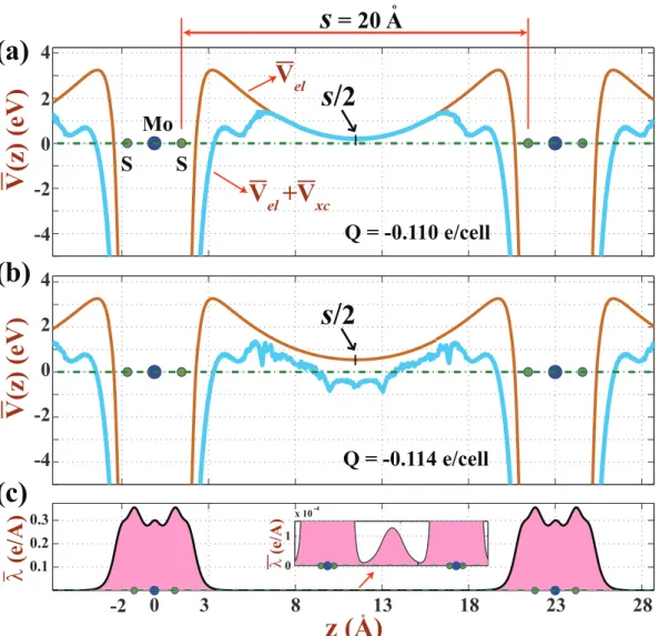
two negatively charged MoS2 layers corresponding to Q=-0.110
e/unit cell before the spilling of electrons into vacuum. The spac-ing between MoS2 layers is s = 20 ˚A. (b) Same as (d) but
Q=-0.114 e/unit cell, where the total potential energy dips below EF
and hence excess electrons start to fill the states localized in the potential well between two MoS2 layers. (c) Corresponding
pla-narly averaged charge density ¯λ. Accumulation of the charge at the center of s is resolved in a fine scale. Arrows indicate the ex-tremum points of ¯Vel(z) in the vacuum region for Q > 0 and Q < 0
cases. . . 29 3.9 (a) Energy eigenvalues of the occupied electronic states, Ei and
corresponding |Ψi(z)|2 are obtained by the numerical solution of
the Schrodinger equation of a planarly averaged, 1D electronic po-tential energy of single layer graphene for s=12.5 ˚A , 25 ˚A and 50 ˚A shown by dashed lines. (b) Same as (a) for 3-layer graphene. Zeros of |Ψi(z)|2 at large z are aligned with the corresponding
en-ergy eigenvalues. . . 31 3.10 Energy band structures of 2D single layer of fluorographene CF,
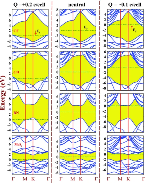
graphane CH, BN and MoS2 calculated for Q = +0.2 e/cell, Q = 0
(neutral) and Q = −0.10 e/cell. Zero of energy is set at the Fermi level indicated by dash-dotted lines. The band gap is shaded. Note that band gap increases under positive charging. Parabolic bands descending and touching the Fermi level for Q < 0 are free electron like bands. Band calculations are carried out for s=20 ˚A. . . 33
LIST OF FIGURES xiv
3.11 (a) Variation of the ratio of lattice constants a of positively charged single layer graphene, BN, CH, CF and MoS2 to their neutral
val-ues aowith the average surface charge density, ¯σ. The unit cell and
the lattice vectors are described by inset. (b) The charge density contour plots in a plane passing through a C-C bond. (c) Same as B-N bond. . . 34 3.12 Exfoliation of graphene layers from both surfaces of a 3-layer
graphite slab (in AB-stacking) caused by electron removal. Isosur-faces of difference charge density, ∆ρ, show the electron depletion. The excess charge on the negatively charged slab is not sufficient for exfoliation. The distributions of planar averaged charge density (λ) perpendicular to the graphene plane are shown below both for positive and negative charging. . . 36 3.13 Variation of planarly averaged positive excess charge ¯λ(z) along
z-axis perpendicular to the BN-layers calculated for different s. As s increases more excess charge is transferred from center region to the surface planes. . . 39 3.14 Variation of cohesive energy and perpendicular force F⊥ in 3-layer
BN slab as a function of the distance L between the surfaces. En-ergies and forces are calculated for different levels of excess positive charge Q (e/unit cell). Zero of energy corresponds to the energy as L → ∞. . . 41 3.15 Exfoliation of outermost layers from layered BN and MoS2 slabs
by positively charging of slabs. (a) Turquoise isosurfaces of excess positive charge density. (b) Change in total energy with excess surface charge density. (c) Variation of L of slabs with charging. 42
3.16 Effect of charging on graphene flake consisting of 78 carbon atoms. (a) Isosurfaces of difference charge density ∆ρ of positively charged, neutral and negatively charged slabs. (b) Corresponding spin-polarized energy level structure. Solid and continuous levels show spin up and spin down states. Red and black levels indicate filled and empty states, respectively. Distribution of magnetic mo-ments at the zigzag edges are shown by insets. Zero of energy is set to Fermi level.(c) Variation of binding energy and net magnetic moment of specific adatoms adsorbed in two different positions, namely A-site and B-site indicated in (a). . . 45 3.17 The comparison of the energy band structures of neutral graphene
calculated with VASP, SIESTA and DFTB. The Fermi level is set to zero energy. The unit cell parameters are same for each calculation. . . 47 3.18 (a) Band structures of charged graphene when 0.2 electron is added
to the unit cell calculated with VASP, SIESTA and DFTB+. The Fermi level is set to zero energy. The unit cell parameters are same for each calculation. (b) Planarly averaged total potential energy, V(z), calculated with plane-wave basis VASP and atomic-orbital basis SIESTA. The carbon atoms are at z = 5 ˚A and length of unit cell along z-direction is 20 ˚A . (c) Planarly averaged total charge density calculated with VASP. . . 49
LIST OF FIGURES xvi
4.1 Various critical sites of adsorption on the 2D honeycomb structure of graphene and an oxygen atom adsorbed on the bridge site, which is found to be as the energetically most favorable site. Carbon and oxygen atoms are shown by gray and red balls, respectively. (b) Variation of energy of oxygen adatom adsorbed to graphene along H → T → B directions of the hexagon. The diffusion path of a single oxygen adatom is shown by stars. (c) Charge density iso-surfaces, isovalues and contour plots of oxygen adsorbed graphene in a plane passing through C-O-C atoms. (d) Same as (c) on the lateral plane of honeycomb structure. (e) Total and partial density of states projected to carbon and oxygen atoms. Calculations are carried out for supercell presented in (c) where O-O interaction is significantly small. . . 54 4.2 (a) Charge density isosurfaces in a rectangular supercell
contain-ing 128 carbon atoms and a scontain-ingle adsorbed O atom shown by a red dot. Bi,j identifies a specific C-C bond, where i indicates the
total number of oxygen atoms in the supercell and j labels some of the bond around adsorbed oxygen atom(s). (b)-(c) and (d) are same as (a), except that 2,3, and 4 oxygen atoms are adsorbed to the sites, which are most favorable energetically. For each new adatom implemented in the system the site which is energetically most favorable is determined by comparing the total energies cor-responding to one of all the available sites. (e) Lowest energy configurations of 5 to 12 oxygen adsorbed on graphene. (f) Varia-tion of the binding energy of the last oxygen adatom for the cases (a)-(e). . . 59 4.3 Adsorption of two oxygen atoms on one surface of graphene with
buckling of 0.88 ˚A. (b) Adsorption of two oxygen atoms at both sides with a buckling of 0.25 ˚A. (c) Isosurfaces of bond charge den-sities after the adsorption of two oxygen atoms, each one adsorbed to different sides of graphene. . . 61
4.4 (a) The bonding configuration of a single carbon atom on graphene and the resulting redistribution of bond charges shown by isosur-faces. (b) The bonding configuration of a single fluorine adatom on graphene with energetically favorable top site. The resulting charges of C-C bonds at close proximity are shown by isosurfaces. (c) The growth pattern in the course of the fluorination of graphene. 64 4.5 (a) The interaction energy between two free oxygen atoms
ap-proaching each other from a distance. The distance between them is dO−O. (b) The interaction energy between a single oxygen atom
adsorbed at the bridge site and a free oxygen atom approaching from the top. Different positions of approaching O atom are shown in the side views. (c) Variation of the energy between two oxygen adatoms on graphene. Some of the positions of the approaching oxygen atom on the path of minimum energy barrier are labeled by numerals ( I-VII ). Top and side views of the configuration of two oxygen atoms are shown by insets. . . 66 4.6 (a) Bare graphene and its typical density of states with zero state
density at the Fermi level EF. The constant energy surfaces of
conduction and valence bands are shown on left-hand side. (b) A four-adatom domain corresponding to lowest total energy con-figuration and has a band gap of 70 meV. (c) Another adsorption configuration of four oxygen adatom resulting in a band gap of 127 meV. (d) A uniform and symmetric configuration of adsorbed oxy-gen atoms with zero density of states at EF. (e) A sizable band gap
is opened when the symmetry of oxygen decoration is broken by the removal of a single oxygen atom. (f) The wide band gap of 3.25 eV is opened at full coverage corresponding to Θ = NO/NC = 0.5
(NO and NC are the numbers of oxygen and carbon atoms in the
LIST OF FIGURES xviii
5.1 (a) Description of 5x5 graphene lattice containing an oxygen atom adsorbed on a bridge site. Periodic bondary conditions are applied. The length of supercell along z-direction is c = 20 ˚A . The carbon (oxygen) atoms are represented by brown (red) filled circles. (b) Planarly averaged total potential energy, V(z), profile for neutral case corresponding to structure in (a). (c) same as (b) when 1.0 electron is added to the unit cell and planarly averaged total charge density profile containing 207 electrons when integrated along direction. (d) same as (c) when the length of unit cell along z-direction is doubled. . . 71 5.2 (a) Equilibrium (bridge) and transition (top) state geometries
for an oxygen atom (red) is adsorbed on graphene (brown) (b) NEB energy barriers corresponding to different charging amounts. The first and last configuration corresponds to equilibrium state (bridge). The length of supercell along z-direction is 20 ˚A . (c) The variation of energy barrier upon increasing the unit cell length from c=20 to c=50 ˚A for 1.0 electron is added. . . 74 5.3 (a) The atomic structure and path of oxygen atom on graphene
folloewd in an 5x5 supercell. (c) Comparision of energy profiles obtained by VASP, SIESTA and DFTB+ calculations for neu-tral case. The variation of energy of oxygen adatom adsorbed on graphene along H-B-T-H directions shown in part (a). (c) the variation of energy for negative and positive charging obtained by DFTB+ calculations. (d) same as (c) obtained by VASP calcula-tions. . . 76
5.4 The energy profile for an oxygen moving towards another station-ary oxygen on graphene for positive charging (1 electron removed, red squares), neutral (green circles) and negative charging (1 elec-tron added, blue triangles). Some of the positions of the approach-ing oxygen atom are labeled by numbers (A-J). Startapproach-ing point ( A ) energy is set to zero. The atomic configurations of G, H=I and J are given below. . . 78
List of Tables
3.1 Dependence of the threshold charges on the vacuum spacing s (˚A) between 3-layer slabs. Threshold charge, Qe (e/cell) where
exfo-liation sets in and corresponding threshold average surface charge density ¯σe = Qe/A (C/m2) are calculated for positive charged
3-layer Graphene, BN and MoS2 sheets for s=50 ˚A and s=20 ˚A.
The numbers of valence electrons per unit cell of the slab are also given in the second column. . . 38
Introduction
The advancement of science strongly depends on the interplay between theoretical and experimental studies. In some cases, theoretical physics sticks to mathemati-cal rigors while giving little importance to observations and experiments. On the other hand, experimental physics sometimes cannot go beyond reporting labora-tory results lacking the theoretical explanation. When theory meets experiment, remarkable scientific achievements are made possible. A well-known example is photoelectric effect, previously an experimental result lacking a theoretical for-mulation but then explained by Einstein who was awarded by Nobel Prize.
Computational physics is the study and implementation of numerical methods to solve physical problems for which a quantitative theory already exists. It is often regarded as a subdiscipline of theoretical physics but some consider it as an intermediate discipline between theoretical and experimental physics. Computa-tional simulation is an integral part of modern science and the ability to exploit effectively the power offered by computers is therefore essential for scientists. It has taken its place as a method for doing science and has bridged the theory to experiment. Computational and theoretical chemistry may provide fundamental insights into the structural properties, reactivities and dynamics of molecules and solids. As a result, theoretical calculations have become essential in various fields of chemical research and development.
CHAPTER 1. INTRODUCTION 2
The motivation of this thesis is stimulated by experimental work done by Ekiz and his co-workers[1] from Prof. Dana’s research group in our home institu-tion claiming that the electrical charge has strong effects on the thermodynamics equilibrium of graphene/graphene-oxide system. They show that in ambient at-mosphere, the positive charge causes oxidation of graphene, and negative charge enhances the reduction of graphene oxide to graphene. Their results suggest that the electrical bias and charging effects are important in energetic analysis and al-low designing of novel graphene-based nanostructures. We present our research in the area of computational physics based on state-of-the-art quantum mechanical simulations in order to better understand these experimental findings.
Recent advances in materials growth and control techniques have made the synthesis of the isolated, two-dimensional (2D) honeycomb crystal of graphene possible [2, 3, 4, 5] in 2004 which was believed to be unstable for a long time[6]. Owing to its unusual electronic energy band structure leading to the charge car-riers resembling massless Dirac Fermions, graphene introduced new concepts and initiated active research [7, 8]. To the best of our knowledge, the effects of static charging on graphene structure haven’t been studied previously and we first start with investigation of the effects of charging on bare graphene structure. Since the graphene structure is recently discovered, through understanding of the effects of charging on graphene is essential from our points of view in order to better under-stand its fundamental physics and developing useful applications. Boron nitride (BN) analogue of graphene were also realized experimentally having desired in-sulating characteristics[9]. Subsequently other graphene like 2D nanostructures have been realized experimentally. Graphane (CH) is hydrogenated form of 2D graphene where each carbon atom bonds with a hydrogen atom[10] and fluoro-graphene (CF) is fluorinated analogue of graphane[11]. Molybenum disulfide, MoS2[12], is another two-dimensional honeycomb structure but not containing
any first and second row elements of periodic table. We call these graphene-like structures as “graphene’s cousins” and investigate the effects of charging on them in addition to graphene. The exfoliation of 3-layered graphene, BN and MoS2 upon positive charging have also been investigated.
performed an extensive analysis of the oxygen adatom adsorption for neutral case. Despite the oxidized graphite is a known material since 150 years and great deal of experimental and theoretical research carried out recently, a precise knowledge regarding the interaction of oxygen with graphene and resulting processes are not available yet. From our point of view, there exists still a controversies between theory and experiment. For example, the distribution of hydroxy and epoxy groups on GOX surface is still unclear; their clustering or uniform coverage trends are unknown. At least, a rigorous explanation for the reason of the differences in the interpretations of experimental data is required.
We finally investigate the effects of charging on the oxidation properties of graphene. The variation of oxidation dynamics with positive and negative charg-ing is studied. Although there are several studies involvcharg-ing charged surface cal-culations available in literature, the deficiencies of using plane-wave calcal-culations in the treatment of negatively charged layers are not emphasized in those works. We clarified those deficiencies and presented alternative ways of dealing with charged calculations in addition to plane-wave calculations. We carried out bind-ing energy and oxygen-oxygen interaction calculations in order to understand the releasing of oxygen atoms from graphene upon negative charging as claimed by experimental study.
The organization of thesis is as follows: Chapter 2 briefly describes the theo-retical background and approximations of the computational methods. Chapter 3 is related with the effects of charging on graphene and graphene-like nanostruc-tures not including graphene-oxide. Chapter 4 is related with the oxidation of graphene while in Chapter 5 we present our results for the effects of charging on the oxidation properties of graphene. Chapter 5 is conclusions summarizing the results of our studies.
Chapter 2
Methodological background
In this chapter we will briefly discuss the theoretical framework, computational methodologies and approximations of density functional theory (DFT) which have been used in this thesis. It is not intended to give complete introduction to DFT calculations but rather to cover some of basic definitions, which are relevant to interpretation of the simulation results. For more detailed and extensive infor-mation the interested reader referred to Payne et al. [13] and references therein.
2.1
Schr¨
odinger Equation and Density
Func-tional Theory (DFT)
The Schr¨odinger equation (SE) is an equation that describes how the quantum state of a physical system changes with time. It was formulated in late 1925, and published in 1926, by the Austrian physicist Erwin Schr¨odinger. The wave function is the solution to the wave equation which is known as the Schr¨odinger equation: " ¯h2 2m∇ 2(r) + V (r) # ψ(r, t) = i¯h∂ψ(r, t) ∂t (2.1) 4
Where m is the particle’s mass, V is its potential energy, ∇2 is tha Laplacian
and ψ is position-space wavefunction. In the standard interpretation of quantum mechanics, the wave function is the most complete description that can be given to a physical system. While SE is believed to hold true for any system, solution of this equation is not feasible in many cases and approximations are used.
The time-independent Schrdinger equation is the equation describing station-ary states and it is easier to solve. By dropping the time dependency, SE gets an eigenvalue equation:
ˆ
HΨi(r,R) = EiΨi(r,R) (2.2)
ˆ
H is the Hamiltonian operator and Ei is the energy eigenvalue
correspond-ing to many body time-independent wave function, Ψi(r,R) . With the aid of
Born-Oppenheimer approximation, in which the electrons are assumed to move faster than the nuclei as a result of significant mass difference between electron and proton (∼1800 times), the nuclei can be treated as stationary. With these conditions, the wave function can be factorized as Ψtotal = ψelectronic× ψnuclear.
Assuming these approximations, we are left with the problem of solving the many-body electronic Schr¨odinger equation for fixed nuclear positions. The resulting Hamiltonian operator for Eqn. 2.2 can be written as:
ˆ
H = ˆTe+ ˆVn−e+ ˆVe−e+ ˆVn−n (2.3)
The first term is the kinetic energy operator for electrons,
ˆ Te = − N X i=1 ¯h2 2m∇ 2 i (2.4)
The second term is the energy operator for ion-electron interactions,
ˆ Vn−e = −e2 P X I=1 N X i=1 ZI |RI − ri| (2.5)
CHAPTER 2. METHODOLOGICAL BACKGROUND 6
in which the charge of Ith ion is represented by Z
I and ri and RI are the
positions of the ith electron and Ith nuclei ion. The third term is a potential
energy operator for the electron-electron interactions:
ˆ Ve−e = e2 2 N X i=1 N X j6=i 1 |ri− rj| (2.6)
The last term corresponds to ion-ion interactions which can be dropped in solving the electronic wave function since it is simply an additive term.
ˆ Vn−n= e2 2 P X I=1 P X J6=I ZIZJ |RI − RJ| (2.7)
where R = {RI}, I = 1, ..., P, is a set of P nuclear coordinates and r =
{rI}, i = 1, ..., N, is a set of N electronic coordinates. The total energy of
the system, Etotal , can be obtained by solving the Eqn. 2.2 for the electronic
ground state energy, Ei, and the ground state many-body wave function Ψi(r,R)
and adding the ion-ion interaction energy term: Etotal = E + Vn−n. Even in
time-independent regime, SE is still very hard to solve and for this reason the effort is directed towards finding more efficient approaches and approximations. Density functional theory (DFT), which has been very popular for calculations in condensed matter physics, is developed for this aim.
DFT has its roots in the Thomas-Fermi (T-F) Approximation [14, 15] which model the electron density as the central variable rather than the wave function. Later a firm theoretical footing by the Hohenberg-Kohn theorems in 1964 [16, 17] was done. The first of these demonstrates the existence of a one-to-one mapping between the ground state electron density and the ground state wave function of a many-particle system. Further, the second Hohenberg-Kohn theorem proves that the ground state density minimizes the total electronic energy of the system. DFT is an alternative approach to the theory of electronic structure, in which the electron density distribution ρ(r) rather than many-electron wave function plays a central role. In the spirit of Thomas-Fermi theory, it is suggested that a knowledge of the ground state density of ρ(r) for any electronic system uniquely
determines the system.
The Hohenberg-Kohn [16] formulation of DFT can be explained by two the-orems:
Theorem 1: For any system of interacting particles in an external potential Vext(~r), the density is uniquely determined except for a trivial additive constant
( in other words, the external potential is unique functional of charge density). Since ρ(r) determines V(r), then it also determines the ground state wave function and gives us the full Hamiltonian for the electronic system.
Theorem 2: A universal functional for the energy E can be dened in terms of the density. The exact ground state is the global minimum value of this functional.
In 1965, W. Kohn and L. Sham [17] proposed the idea of replacing the kinetic energy of the interacting electrons with that of an equivalent non-interacting system. With this assumption density can be written as:
ρ(r) = 2 X s=1 Ns X i=1 |ϕi,s(r)|2 (2.8)
With the kinetic energy term:
T [ρ] = 2 X s=1 Ns X i=1 hϕi,s| − ∇ 2 2 |ϕi,si (2.9)
The single-particle orbitals ϕi,s‘s are the NS lowest order eigenfunctions of
Hamiltonian that is
{−∇
2
2 + v(r)}ϕi,s(r) = ǫi,sϕi,s(r) (2.10)
Using new form of T [ρ], the universal density functional can be written in the following form:
CHAPTER 2. METHODOLOGICAL BACKGROUND 8 F [ρ] = T [ρ] + 1 2 Z Z ρ(r)ρ(r′) |r − r′| drdr ′+ E XC[ρ] (2.11)
where this equation defines the exchange and correlation energy as a functional of the density. Using this functional in the total energy functional, E[ρ] = F[ρ] + R
ρ(r)v(r)dr we finally obtain the total energy functional which is known as Kohn-Sham functional: [17] EKS[ρ] = T [ρ] + Z ρ(r)v(r)dr + 1 2 Z Z ρ(r)ρ(r′) |r − r′| drdr ′+ E XC[ρ] (2.12)
In this way the density functional is expressed in terms of the KS orbitals, which minimize the kinetic energy under the fixed density constraint. In princi-ple, these orbitals are a mathematical object constructed in order to render the problem more tractable and do not have any sense by themselves, but only in terms of the electronic density. The solution of KS equations can be obtained by an iterative way, in the same way of Hartree and Hartree-Fock equations. In practice, however, it is customary to consider KS orbitals as single-particle physical eigenstates.
In summary, we briefly described the theory that is able to solve the com-plicated many-body problem by mapping exactly the many-body Schroedinger equation into a set of coupled single-particle equations. Given an external po-tential, the energy and any desired ground state properties (e.g., stress, phonons, etc.) can be obtained. The density of the non-interacting reference system is equal to that of the true interacting system. Up to now the theory is exact since have not introduced any approximation into the electronic problem. All the ig-norance about the many-body problem has been displaced to the EXC [ρ] term,
while the remaining terms in the energy are known.
In the next sections we discuss the approximations employed for solving KS equations.
2.2
Exchange-Correlation Functionals
The main approximation enters in the choice of an exchange-correlation func-tional, EXC [ρ], since no exact form is known for this functional. The oldest, the
simplest and widely used is the local density approximation (LDA) suggested by Kohn and Sham. In the LDA approximation the exchange-correlation energy of an electronic system is constructed by assuming that the exchange-correlation energy per electron at a point r in the electron gas, εXC(r), is equal to the
exchange-correlation energy per atom in a homogeneous electron gas that the same density as the electron gas at point r. Thus
ELDA XC [ρ] =
Z
ρ(r)εLDA
XC [ρ]dr (2.13)
The local-density approximation assumes that the exchange-correlation en-ergy is purely local and ignores correlations to the exchange-correlation enen-ergy at a point r due to nearby inhomogeneities in the electron density. Considering the inexact nature of approximation, the calculations performed with LDA is quite successful especially for metals and semiconductors.
As a next step, some of the non-locality can be included by making the εXC
depend also on the gradient(s) of the electron density. Several studies, but es-pecially by Perdew [18], have worked on next step to the LDA with inclusion of effects proportional to the gradient of the charge density. The improvements along these ways are called Generalized Gradient Approximation (GGA). In some systems GGA give better results but worse in others, Generally, the GGA seems to be an improvement over the conventional LDA. The exchange-correlation en-ergy in GGA can be expressed in the following form:
EXC[ρ] =
Z
ρ(r)ǫXC[ρ(r)]dr +
Z
FXC[ρ(r, ∇ρ(r))]dr (2.14)
where the function FXC is asked to satisfy the formal conditions for the
CHAPTER 2. METHODOLOGICAL BACKGROUND 10
2.3
Periodic boundary conditions and
plane-wave basis sets
There are some difficulties arising from mapping of observables of the many-body problem into equivalent observables in an effective single-particle problem. One of them is the wave function which must be calculated for each of infinite number of electrons in the the system. The other one is that the basis set required to expand each wave function is infinite since the wave function extends over the entire solid. Both problems can be solved by performing calculations on periodic systems and applying Bloch’s theorem to the wave functions.
Bloch theorem states that in a periodic solid each electronic wave function can be written as the product of a periodic function and a plane wave envelope function:
Ψi(r) = ui(r)eikr (2.15)
where uk has the period of crystal lattice with uk(r) = uk(r+T). This part can
be expanded using a basis set consisting of reciprocal lattice vectors of the crystal. ui(r) =
X
G
ak,Gei(G)r (2.16)
Therefore each electronic wave function can be written as a sum of plane waves Ψi(r) =
X
G
ai,k+Gei(k+G)r (2.17)
In principle, an infinite number of plane-waves are required to expand the wave function at each k-point in above sum. However, only the small kinetic energy terms are important. For this reason, an energy cut-off (Ecutof f) can be
imposed on plane waves such that |k + G|2 < E
cutof f. Furthermore, increase or
2.4
Pseudopotential approximation
Although Bloch’s theorem states that every electronic wave function can be ex-pressed using a discrete set of plane waves, it is sometimes very poorly suited to expand wave functions because a very large number of plane waves are needed to expand the tightly bounded core electrons. An extremely large plane-wave basis set may be required to perform all-electron calculation leading to a vast amount of computational time to calculate electronic wave functions. Pseudopotential approximation allows the expansion of electronic wave functions using a much smaller plane-waves.
It is well known that most of the physical properties of solids mainly depends on valance electrons rather than the core electrons. The pseudopotential approx-imation exploits this by removing core electrons and replacing them and strong ionic potential by a weaker pseudopotential that acts on a set of pseudo wave functions rather than the actual valance wave functions.
Chapter 3
Charging of 2D honeycomb
structures
We investigate the effects of static charging on structural, electronic and mag-netic properties of suspended, single layer graphene, graphane, fluorographene, BN and MoS2. All these honeycomb nanostructures have two dimensional (2D)
hexagonal lattice. We demonstrate that the properties of these nanostructures can be modified either by direct electron injection into it or electron removal from it; namely by charging the system externally. The limitations of periodic boundary conditions in the treatment of negatively charged layers are clarified. Upon positive charging the band gaps between the conduction and valence bands increase, but the single layer nanostructures become metallic owing to the Fermi level dipping below the maximum of valence band. Moreover, their bond lengths increase leading to phonon softening. As a result, the frequencies of Raman active modes are lowered. High level of positive charging leads to structural instabilities in single layer nanostructures, since their specific phonon modes attain imaginary frequencies. Similarly, excess positive charge is accumulated at the outermost lay-ers of metallized BN and MoS2 sheets comprising a few layers. Once the charging
exceeds a threshold value the outermost layers are exfoliated. This result may be exploited to develop a method for intact exfoliation of graphene and these graphene-like structures. Charge relocation and repulsive force generation are in
compliance with classical theories. In addition to exfoliation, the energy level structure, density of states, binding energies and desorption of specific adatoms can be monitored by charging. We found that pseudopotential plane-wave cal-culations of charged surfaces using periodically repeating layers are sensitive to the vacuum spacing between adjacent cells and have limited applicability. On the other hand, using atomic-orbital based methods was shown to have some advantages.
In the following sections we briefly describe some of structural and electronic properties of graphene, BN, MoS2, CH and CF. Then we present our results on
the effects of charging of these structures.
3.0.1
Graphene and its structure
Synthesis of a single atomic plane of graphite, i.e. graphene, with covalently bonded honeycomb lattice has been a breakthrough for several reasons[2, 3, 4, 5, 19]. Firstly, electrons behaving as if massless Dirac fermions have made the observation of several relativistic effects possible. Secondly, stable graphene has disproved previous theories, which were concluded that two-dimensional struc-tures cannot be stable. Graphene with its unique mechanical, structural, elec-tronic and thermal properties has been identified as a promising candidate for novel applications in various fields[8], Not only 2D graphene, but also its quasi 1D forms, such as armchair and zigzag nanoribbons have shown novel electronic and magnetic properties[20, 21, 22], which can lead to important applications in nanotechnology. Up to now, many of its unusual properties are well investi-gated and clever methods of graphene production are proposed[23, 24, 25, 26, 27], Further studies are directed towards the controlling of graphene’s electronic and magnetic properties in order to open the new ways of better understanding of its fundamental physics and developing useful applications.
The hexagoanal lattice structure and reciprocal lattice of graphene are shown in Fig. 3.1. The lattice vectors can be written as:
CHAPTER 3. CHARGING OF 2D HONEYCOMB STRUCTURES 14 ~a1 = a 2( √ 3, 3, 0) ~a2 = a 2(− √ 3, 3, 0) (3.1)
where a ≈ 1.42 ˚A is the nearest carbon-carbon distance. The reciprocal lattice vectors are given by:
~b1 = 2π 3a( √ 3, 1, 0) ~b2 = 2π 3a(− √ 3, 1, 0) (3.2)
The two points at the corners of graphene’s Brillouin zone (BZ) is of special importance. Their positions are given by:
K= 2π 3√3a, 2π 3a, 0 ! K’= − 2π 3√3a, 2π 3a, 0 ! (3.3)
These special points are called Dirac points and are of particular importance for the electronic properties. Graphene is a semimetal having conduction and valance bands crossing linearly at K-point at the Fermi level (EF) as shown in
Fig. 3.1 (c). The resulting electron-hole symmetry reveals itself in an ambipolar electric field effect, whereby under bias voltage the charge carriers can be tuned continuously between electrons and holes in significant concentrations. Due to its planar 2D structure and reactant pz orbitals, graphene is naturally responsive for
the addition of adsorbates. Graphene oxide (GOX) is a pronounced example[28]. Excess electrons and holes can be also achieved through doping with foreign atoms[29, 30, 31]. For example, adsorbed alkali atoms tend to donate their va-lence electrons to π∗-bands of graphene. The excess electrons results in the
met-alization of graphene[32]. Hole doping is achieved by the adsorption of bismuth or antimony[33]. However, the system remains electrically neutral through either way of doping. Recently, carrier concentration and spatial distribution of charge are also changed for very short time intervals by photoexcitation of electrons from the filled states leading to the photoexfoliation of graphite[34, 35, 36].
a1 b1 b2 K’ K M Γ x y a2 kx ky (a) (b) -8 -6 -4 -2 0 2 4 6 8
M
Γ
K
Γ
En
er
gy (e
V
)
(c)E
FFigure 3.1: (a) Primitive unit cell of the honeycomb structure of graphene. (b) reciprocal lattice vectors and corresponding Brillouin zone (BZ) having special k-points Γ, M and K. (c) Calculated electronic band structure of graphene.
CHAPTER 3. CHARGING OF 2D HONEYCOMB STRUCTURES 16
3.0.2
Graphene’s cousins : BN, MoS
2, CH and CF
Boron nitride (BN) in ionic honeycomb lattice which is the Group III-V analogue of graphene have also been produced having desired insulator characteristics[9]. Nanosheets[37, 38], nanocones[39], nanotubes[40], nanohorns[41], nanorods[42] and nanowires[43] of BN have already been synthesized and these systems might hold promise for novel technological applications. Among all these different struc-tures, BN nanoribbons, where the charge carriers are confined in two dimension and free to move in third direction, are particularly important due to their well defined geometry and possible ease of manipulation.
BN nanoribbons posses different electronic and magnetic properties depending on their size and edge termination. Recently, the variation of band gaps of BN nanoribbons with their widths and Stark effect due to applied electric field have been studied[44, 45]. The magnetic properties of zigzag BN nanoribbons have been investigated[46]. Half-metallic properties have been revealed from these studies which might be important for spintronic applications.
The atomic structure, atomic charge, charge transfer from B to N and the electronic structure of 2D BN are presented in Fig. 3.2. Contour plots of total charge indicates high density around N atoms. The difference charge density is calculated by subtracting charge densities of free B and N atoms from the charge density of 2D BN, i.e. ∆ρ = ρBN − ρB− ρN. High density contour plots around
N atoms protruding towards the B-N bonds indicate charge transfer from B to N atoms. This way the B-N bonds achieve an ionic character[47]. The amount of transfer of charge is calculated by L¨owdin analysis to be ∆Q=0.429 electrons.
2D BN is a semiconductor[47]. Calculated electronic energy bands are similar to those calculated for h-BN crystal. The π- and π∗- bands of graphene which
cross at the K- and K′-points of the BZ open a gap in 2D BN as a bonding and antibonding combination of N-pz and B-pz orbitals. The contribution of N-pz is
pronounced for the filled band at the edge of valence band. The calculated band gap is indirect and Egap =4.64 eV[47].
Figure 3.2: (a) Primitive unit cell of the honeycomb structure of 2D BN together with Bravais lattice vectors. Calculated total charge density ρBN and difference
charge density ∆ρ, are also shown in the same panel. (b) Calculated electronic structure of 2D BN honeycomb crystal together with total, TDOS and partial density of states, PDOS on B and N atoms. The orbital character of the states are also indicated.
CHAPTER 3. CHARGING OF 2D HONEYCOMB STRUCTURES 18
(a)
(b)
Mo
S
a1 a2Figure 3.3: (a) Atomic structure of 1H-MoS2 in hexagonal lattice from top and
side view. The unit cell is shaded and lattice constants are indicated. (b) Atomic structure for three dimensional bulk MoS2. Purple (large) and yellow (small)
balls denotes Molybenum and Sulfur atoms.
Molybenum disulfide, MoS2, is made up of hexagons with Mo and S2 atoms
situated at alternating corners. Each S atom has three nearest Mo atom, and each Mo atoms has six nearest S atoms. For the case of three dimensional bulk MoS2 (specified as 1H-MoS2), the layers in the unit cell are displaced relative to
each other , so that Mo atoms of one layer are situated on top of S atoms in the two adjacent layers. In this respect, the arrangements of layers are different from that of graphite, where three carbon atoms of one layer are located above the hollow sites (center of the hexagon) of the adjacent layers. The atomic con-figurations and relevant structural parameters of two-layer MoS2 are illustrated
in Fig. 3.3 Recently, two-dimensional suspended single-layer MoS2 sheets have
been produced[9, 48]. Single-layer MoS2 nanocrystals having ∼ 30 ˚A width were
a
1a
2 H C dC-C=1.52 A dC-H=1.12 A dC-C d C-H 0 0Graphane
Figure 3.4: Schematic representation of the atomic structure of graphane. The unit cell is shaded and lattice constants are indicated.
The in-plane lattice constant, |~a1| = |~a2|, is 3.22 ˚A both for 1H- and
2H-MoS2 calculated with GGA method including vdW interactions[50]. The other
lattice constant, |c|, is 12.411 ˚A for 2H-MoS2 but increases to 15.540 with the
inclusion of vdW interactions[50]. The electronic structure of hexagonal MoS2 is
semiconductor. 3D bulk MoS2 has a indirect band gap of 0.85 eV while 1H-MoS2
has a direct band gap of 1.58 eV calculated by GGA method.[51] Furthermore, these band gap values increases to 2.50 and 1.44 eV with GW0 calculations[51].
We recently revealed that weak vdW interaction between layers is critical to hold the layers together and to calculate the interlayer spacing within 0.8% of the experimental value[50]. Therefore, the inclusion of the vdW interaction between the layers of MoS2 is found to be essential for ab initio calculations of energetics
and optimized structures, cohesion, and phonon dispersions.
Graphane (CH), is another member of honeycomb structures was theoretically predicted[52] and recently synthesized by exposing graphene to hydrogen plasma discharge[10]. Here each carbon atom being bonded to one hydrogen atom is pulled out from the graphene plane and hence whole structure is buckled. Instead of being a semimetal like graphene, graphane is a wide band gap semiconductor. Upon hydrogenation of graphene, the lattice constant increases to 2.54 ˚A and d increases to 1.54 ˚A[10]. Moreover, C-H bonds are 1.11 ˚A and the amount
CHAPTER 3. CHARGING OF 2D HONEYCOMB STRUCTURES 20
of buckling between the alternating carbon atoms in a hexagon is 0.46 ˚A[53]. Atomic configuration of graphane structures is shown in Fig. 3.4. The calculated band gap by GGA method is 3.54 eV for graphane[53]. However, the band gap increases to 5.66 eV after G0W0 corrections[53].
We showed that the in-plane stiffness value and Poisson ratio of graphane are 243 J/m2 and 0.07 respectively[53]. Compared to graphene and other 2D
materials, these values indicate that it has a quite high in-plane stiffness and very low, perhaps the lowest Poisson’s ratio among known monolayer honeycomb structures. We also showed that the band gap of graphane can be modified significantly by applied strain in the elastic range. It is suggested that elastic deformation can be used for further functionalization of graphane and hence for monitoring its chemical and electronic properties[53].
Much recently, Nair and his co-workers[11] synthesized fluorinated graphene (CF) and reported the measured Raman spectrum, band gap, Young’s modulus and breaking strength. Each carbon atom of graphene can bind only one F atom, and through coverage (or decoration) of one or two sides of graphene, one can achieve diverse structures. Fluorographene (CF), where F atoms are bound to each C atom of graphene alternatingly from top and bottom sides, is energetically the most favorable structure. Upon full uorination, the planar honeycomb structure of C atoms becomes buckled (puckered) and the C-C bond length increases by ∼ 10%. At the end, while planar sp2 bonding of graphene is
dehybridized, the buckled conguration is maintained by sp3 -like rehybridization.
Our calculated lattice constant for CF is 2.55 ˚A and the in-plane stiffness is 250 (J/m2)[87]. Atomic configuration of CF is shown in Fig. 3.5.
Similar to CH, fully fluorinated graphene, CF, is a wide band gap insulator. While LDA calculations yield a band gap of 2.96 eV GW0 calculations increase
the band gap as high as 7.49 eV[54].
Single layer graphene, graphane CH, fluorographene CF, BN and MoS2 have
displayed unusual chemical and physical properties for future nanotechnology ap-plications. Furthermore, the properties of these nanomaterials can be modified by creating excess electrical charge. Linear crossing of bands of graphene at the
Fluorographene
F C x dC-C=1.55 A dC-F=1.37 A 0 0 a1 a2Figure 3.5: Schematic representation of the atomic structure of fluorographene. The unit cell is shaded and lattice constants are indicated.
Fermi level gives rise to electron-hole symmetry, whereby under bias voltage the charge carriers can be tuned continuously between electrons and holes in signif-icant concentrations. This way, the conductivity of graphene can be monitored. Similar situation leading to excess electrons or holes can also be achieved through doping with foreign atoms. Layered materials can be exfoliated under excessive charging, which is created by photoexcitation for very short time. It is proposed that the femtosecond laser pulses rapidly generate hot electron gas, which spills out leaving behind a positively charged graphite slab. Eventually, charged out-ermost layers of graphite are exfoliated.
3.1
Computational Methodology
Three different first-principles simulation packages; VASP[55, 56], SIESTA[57, 58] and DFTB+[59, 60] are used in this thesis study.
VASP calculations are carried out within spin-polarized and spin-unpolarized density functional theory (DFT) using projector-augmented wave potentials[61]. For the calculations in Sec. 3.2 and 3.7 the exchange correlation potential
CHAPTER 3. CHARGING OF 2D HONEYCOMB STRUCTURES 22
is approximated by local-density approximation (LDA). For the rest of calcu-lations the generalized gradient approximation (GGA) is used[62]. We also per-formed GGA+vdW (generalized gradient approximation including van der Waals corrections[63]) for a better account of van der Waals (vdW) interlayer interac-tions between graphene, BN and MoS2 slabs. A plane-wave basis set with kinetic
energy cutoff of 500 eV is used. All atomic positions and lattice constants are optimized by using the conjugate gradient method, where the total energy and atomic forces are minimized. The convergence for energy is chosen as 10−5 eV
between two steps, and the maximum force allowed on each atom is less than 0.01 eV/˚A. The Brillouin zone (BZ) is sampled by (15x15x5) special k-points for primitive unit cell and scaled according to the size of supercells.
The calculations with SIESTA where the eigenstates of the Kohn-Sham hamil-tonian are expressed as linear combinations of numerical atomic orbitals are per-formed. The exchange-correlation functional of the generalized gradient approx-imation is represented by the PBE approxapprox-imation[64]. A 200 Ryd mesh cut-off is chosen and the self-consistent calculations are performed with a mixing rate of 0.1. Core electrons are replaced by norm-conserving, nonlocal Truoiller-Martins pseudopotentials. The convergence criterion for the density matrix is taken as 10−4.
The Density Functional based Tight binding method (DFTB+) is based on a second-order expansion of the Kohn-Sham total energy in Density-Functional Theory (DFT) with respect to charge density fluctuations. In this approach, the reference electron density is obtained self-consistently from weakly confined neutral atoms and the confinement potential is optimized to predict the effective potential and charge density for molecules and solids. A minimal basis set is established tight-binding matrix elements are explicitly calculated within DFT framework. The DFTB+ program is orders of magnitude faster than standart DFT methods, but requires parameter files to be installed for all pair-wise com-binations of atoms in a molecule or solid. In this work, the SlaterKoster (S-K) type parameter set[65] was implemented. All of our DFTB+ calculations only include s- and p-orbital interactions.
Adatom and graphene system breaks inversion symmetry and a net electric-dipole moment is generated perpendicular to the graphene surface. Dipole corrections[66] are applied in order to remove spurious dipole interactions be-tween periodic images for the neutral calculations.
We add or remove electrons from the unit cell in order to simulate electron and hole doping. This is widely used method[67, 68, 69, 70] to simulate the effect applying a gate voltage to graphene-adatom system by changing the num-ber of electrons. Normally, periodic boundary conditions realized by repeating charged supercells has a divergent electric potential energy and has drawbacks and limitations, which have been the subject matter of several studies in the past. To achieve the convergence of electronic potential, additional neutralizing background charge is applied[71, 66].
The amount of charging, ρ, is specified as either positive charging, i.e. electron depletion (ρ > 0), or negative charging, i.e. excess electrons, in units of ± electron (e) per number of atoms or per unit cell. Average surface charge density is specified as ¯σ = Q/A, i.e the charge per unit area, A, being the area of the unit cell.
It will be informative briefly discussing some works about charged calcula-tions available in literature. Poloni and his co-workers[72] study the interplay between charge doping and intermolecular distance in the polymerization of C60
fullerene chains of using SIESTA. They show that the polymerization depends on both the center-to-center distance of fullerenes and the negative doping of the system. In particular, they observed that up to a doping of four electrons per two molecules, the energy barrier which is related to the formation energy of co-valent bonds between fullerenes progressively decreases. Plane-wave calculations with PWscf package by Attaccalite and his co-workers[73] propose a new way of tuning the electron-phonon-coupling (EPC) in graphene by changing the defor-mation potential with electron/hole doping. The doping is simulated by changing the number of electrons in unit cell. They show that the EPC for highest optical branch at the K point in BZ acquires a strong dependency on the doping level due to electron-electron correlation. In another study, density functional tight
CHAPTER 3. CHARGING OF 2D HONEYCOMB STRUCTURES 24
binding simulations (DFTB+) were used to explore the charging of graphene nanoflakes[74]. They try to determine the effective failure limit of graphene with respect to induced anionic charge produced by electron-beam or electric current. They predict that graphene flakes are resistant to high level of charging posing no problem to the operation of graphene-based electronic devices. But the local-ized regions were shown to be transformable from sp2-bonded into sp3-bonded
material before the failure limit. Apart from doping, Ao and his co-workers[75] demonstrate that the applied electric field can significantly facilitate the bind-ing of hydrogen molecules on N-doped graphene through dissociative adsorption and diffusion on graphene surface. By removing the electric field, the stored hy-drogens on graphene can be released efficiently under ambient conditions when the hydrogen concentration is higher than 0.5 wt% which indicates that N-doped graphene can be used as hydrogen storage material with a storage capacity of 6.73 wt%. The electric field calculations were performed using DMOL3 code.
Assuming that varying the number of electrons in a adatom-graphene system can be used to simulate the effects of gate voltage, Chan and his co-workers[67] demonstrate the ionization of a Li and Co adatoms by doping. The ionization is accompanied by a sharp change in the electrostatic potential of the adatom. This results were consistent with recent STS experiments for Co on graphene[68]. In another study carried out using VASP code, Suarez and his co-workers[70] analyze the diffusion of oxygen adatoms on graphene and its dependence on the carrier density controlled by a gate voltage. The energy barrier which is related with the diffusivity of oxygen on graphene was predicted to be strongly dependent on the carrier density.
3.2
Charging of graphene
We first start with charging of graphene structure. Two-dimensional single layer of graphene layers separated with a vacuum space s between them are repeated periodically along the perpendicular z-direction as shown in Fig. 3.6 (a). The unit cell is made up of primitive unit cell containing 2 carbon (C) atoms. a=b is the
EF -8 -6 -4 -2 0 2 4 6 8 -8 -6 -4 -2 0 2 4 6 8 -8 -6 -4 -2 0 2 4 6 8
(b)
ρ = +0.20 (e/atom)(c)
neutral(d)
ρ = -0.05 (e/atom)En er gy (e V ) Γ Μ Κ Γ Height h (A)o
λ
(e
-/A
)
o 0 5 10 15 20 25 30 35 40 45 50 x 10-5 0 1 2 x 10⁻⁴ -4(e)
(f)
Ψ5 Ψ6 Ψ7 Ψ10Ψ
EF EF 0 1 6 2Ψ
52Ψ
10 2Ψ
7 2Ψ
62Ψ
5 2Ψ
7 2Ψ
102λ
(e
-/A
)
o |a| |b| s s c(a)
z x yFigure 3.6: (a) Description of lattice used to treat 2D single layer graphene. a=b, c are the lattice constants, s is the vacuum spacing between adjacent layers. Primitive unit cell is shaded. (b) Energy band structure of positively charged graphene by ρ=+0.20 e/atom. (c) Neutral. (d) Negatively charged graphene by ρ=-0.05 e/atom, where excess electrons start to occupy the surface states. Zero of energy is set to Fermi level. (e) Planarly averaged charge density (λ) of states, Ψ5−10, of neutral graphene. (f) Same as (e) after charging with ρ=-0.05 e/atom.
CHAPTER 3. CHARGING OF 2D HONEYCOMB STRUCTURES 26
lattice constant of supercell in x-y plane and c=s is the distance along z-direction separating periodic graphene planes. The carbon pseudopotential used in this study contains 4 valance electrons. Therefore, there are 8 electrons in a primitive unit cell shown in Fig. 3.6 (a). The calculations are performed for s = 50 ˚A . When 0.4 electron is removed from the unit cell, this corresponds to ρ=+0.20 e/atom or ¯σ= 0.077 (e/A2). Similarly addition of 0.1 electron corresponds to
ρ=-0.05 e/atom or ¯σ= -0.019 (e/A2).
The work function of neutral graphene is calculated to be 4.27 eV. Lowest two parabolic bands Ψ5 and Ψ6 in Fig. 3.6(c) have effective masses m∗=1.05
and 1.02 me (free electron mass) in the xy-plane parallel to the atomic plane of
graphene. Hence they are nearly free electron like (NFE) in 2D , but they are bound above the graphene plane. These ”surface” states[76] can be expressed as ΨS ∼ eikk.rkΦ(z), where rk and kk are in the xy-plane. Parabolic bands at
higher energies becomes NFE in 3D. When the electrons are removed, the Fermi level is lowered from the Dirac point and positively charged graphene attains metallic behavior as in Fig. 3.6(b). At the end, the work function increases. However, under negative charging, whereby electrons are injected to the graphene, Fermi level raises above the Dirac point and eventually becomes pinned by NFE parabolic bands as in Fig. 3.6(d).
The planarly averaged charge density profiles of some of conduction states of neutral graphene is presented in Fig. 3.6 (e) labeled as Ψ5, Ψ6,Ψ7,Ψ10. These
parabolic NFE bands start to get occupied around ρ=-0.015 e/atom (or surface excess charge density ¯σ=-0.0926 C/m2). Upon charging the bound charge of Ψ
S
states are further removed from graphene as shown in Fig. 3.6(f). While the Fermi level of negatively charged graphene rises and then is quickly pinned by the parabolic, nearly free electron like bands, it moves down readily by removal of electrons from graphene.
3.3
Charging of 2D monolayer MoS
2The negative and positive charging of suspended monolayer MoS2 is treated using
supercell method similar to graphene in previous section. In Fig. 3.7 (a) we describe MoS2 single layers, which are periodically repeated along the z-direction
and separated by a vacuum spacing s between the adjacent outermost sulfur planes. In Fig. 3.7 (b) and (c) the self-consistent electronic potential energy, Vel(r) is averaged in the planes perpendicular to the z-axis to obtain planarly
averaged 1D potential energy ¯Vel(z) for different values of s.
In the vacuum region, the electronic potential energy ¯Vel(z) strongly depends
on the vacuum spacing s. For an infinitely large single plane having excess charge Q > 0 per cell, the potential energy in the vacuum region is linear, if it is not periodically repeating. Thus, as z → ∞, ¯Vel(z → ∞) → +∞ as schematically
shown in Fig. 3.7 (b). However, for a periodically repeating single layers (within the periodic boundary conditions) the potential energy is symmetric with respect to the center of vacuum spacing and it passes through a maximum at s/2. The maximum value of the potential increases with increasing s in Fig. 3.7(b).
In contrast, for a negatively (Q < 0 per cell) charged and infinite MoS2
single layer, a reverse situation occurs as shown in Fig. 3.7 (c). Namely ¯Vel(z →
∞) → −∞ linearly, if MoS2 single layer is not periodically repeating. Notably,
the energy of a finite size, single layer nanostructure (i.e. a flake) does not diverge, but has finite value for large z both for Q > 0 and Q < 0 cases. On the other hand, for periodically repeating single layers within the periodic boundary conditions, potential energies are symmetric with respect to the center of vacuum spacing and they passes through a minimum at s/2. This way a potential well is formed in the vacuum region between two adjacent layers. Normally, the depth of this well increases with increasing negative charging and s. At a critical value of negative charge, the self-consistent potential energy V (r) including electronic and exchange-correlation potential energies dip below the Fermi level (even if
¯
Vel(z) > EF) and eventually electrons start to occupy the states localized in the
quantum well. Such a situation is described in Fig. 3.8 (d)-(f). Of course, this situation suffers from the method of using plane-wave basis set and the repeating