Comparative analysis of zinc-blende and wurtzite GaN for full-band polar optical
phonon scattering and negative differential conductivity
C. Bulutay, B. K. Ridley, and N. A. Zakhleniuk
Citation: Appl. Phys. Lett. 77, 2707 (2000); doi: 10.1063/1.1320020 View online: https://doi.org/10.1063/1.1320020
View Table of Contents: http://aip.scitation.org/toc/apl/77/17
Published by the American Institute of Physics
Articles you may be interested in
Transition between wurtzite and zinc-blende GaN: An effect of deposition condition of molecular-beam epitaxy
Applied Physics Letters 89, 151921 (2006); 10.1063/1.2360916
Comparison of zinc-blende and wurtzite GaN semiconductors with spontaneous polarization and piezoelectric field effects
Journal of Applied Physics 87, 353 (2000); 10.1063/1.371915
Electronic transport studies of bulk zincblende and wurtzite phases of GaN based on an ensemble Monte Carlo calculation including a full zone band structure
Journal of Applied Physics 78, 1033 (1995); 10.1063/1.360405
Electronic band structures and effective-mass parameters of wurtzite GaN and InN
Journal of Applied Physics 83, 1429 (1998); 10.1063/1.366847
Band gap engineering of wurtzite and zinc-blende GaN/AlN superlattices from first principles
Journal of Applied Physics 108, 103701 (2010); 10.1063/1.3505752
Deep traps in AlGaN/GaN heterostructures studied by deep level transient spectroscopy: Effect of carbon concentration in GaN buffer layers
Comparative analysis of zinc-blende and wurtzite GaN for full-band polar
optical phonon scattering and negative differential conductivity
C. Bulutaya)and B. K. Ridley
Department of Electronic Systems Engineering, University of Essex, Colchester C04 3SQ, United Kingdom
N. A. Zakhleniuk
Caswell Technology, Marconi Caswell, Towcester, Northants, NN12 8EQ, United Kingdom 共Received 26 May 2000; accepted for publication 1 September 2000兲
For high-power electronics applications, GaN is a promising semiconductor. Under high electric fields, electrons can reach very high energies where polar optical phonon 共POP兲 emission is the dominant scattering mechanism. So, we undertake a full-band analysis of POP scattering of conduction-band electrons based on an empirical pseudopotential band structure. To uncover the directional variations, we compute POP emission rates along high-symmetry directions for the zinc-blende 共ZB兲 crystal phase of GaN. We also compare the results with those of the wurtzite phase. In general, the POP scattering rates in the zinc-blende phase are lower than the wurtzite phase. Our analysis also reveals appreciable directional dependence, with the⌫ – L direction of ZB GaN being least vulnerable to POP scattering, characterized by a scattering time of 11 fs. For both crystal phases, we consider the negative differential conductivity possibilities driven by the negative effective mass part of the band structure. According to our estimation, for the ZB phase the onset of this effect requires fields above ⬃1 MV/cm. © 2000 American Institute of Physics.
关S0003-6951共00兲02743-1兴
The wide-band-gap III-nitride semiconductors are cur-rently being considered for high-power and high-temperature applications. Among these III nitrides, the most studied is GaN which can be grown either in wurtzite 共WZ兲 or zinc-blende共ZB兲 phases depending on the choice of the substrate and the growth conditions.1 The mounting interest in the high-field applications of GaN, brings under demand a de-tailed knowledge of the transport properties, like the charac-terization of the dominant scattering mechanism. This, in GaN is the polar optical phonon 共POP兲 scattering due to its high degree of ionicity.2A realistic high-field analysis inevi-tably requires a full-band treatment as the carriers under the influence of such high fields move further away from the band edge where their scattering rate depends on the details of the band structure.
In this letter, we present a full-band analysis of the POP scattering of conduction-band 共CB兲 electrons based on the empirical pseudopotential band structure. To shed light on the effects of the crystal phase, we consider both ZB and WZ structures. We place more emphasis on the ZB phase, as a comprehensive discussion of the WZ case has been given by us elsewhere.3For the empirical pseudopotential band struc-ture of ZB GaN, we use published form factors,4 however, for the case of WZ GaN we felt the necessity to develop our own form factors3 due to the poor performance of the CB properties of the available ones.
Considering the ZB case, the scattering rate based on Fermi’s Golden Rule due to POP emission of an electron at the band m, with a wave vector k, is given by
Wm共k兲⫽2 ប V 共2兲3
兺
m⬘冕
1st BZ d3k⬘
⌬m⬘,m共k⬘
,k兲⫻兩CPOP共q兲兩2␦共Em⬘共k
⬘
兲⫺Em共k兲⫹បLO兲, 共1兲where the emitted phonon wave vector is q⫽⫺k
⬘
⫹k mapped to first BZ, the primed indices represent final-state electron labels over which a summation/integration is per-formed, V is the total crystal volume, Em(k) is the band energy of the electron, and បLOis the longitudinal-optical共LO兲 phonon energy assumed to be dispersionless. The cubic POP coupling constant is given by 兩CPOP(q)兩2
⫽2e2បLO(⑀⬁⫺1⫺⑀0⫺1)/(V q
2), where ⑀
0 and ⑀⬁ are the
static and high-frequency dielectric constants. The cell-periodic overlap parameter is given by ⌬m⬘,m(k
⬘
,k)⫽兩(1/⍀)兰⍀um*⬘,k⬘(r)um,k(r)d3r兩2, where um,k(r) is the cell-periodic part of the Bloch wave function and⍀ is the volume of the primitive cell. This overlap parameter is vital to ac-count for the restrictions brought by the symmetries of the participating wave functions to the scattering probabilities. For the parameters of GaN, up to room temperature the ther-mal phonon occupation remains negligible, hence, Eq. 共1兲 actually governs the overall scattering rate up to room tem-perature.
We compute the scattering rate in two alternative ways:3 by direct integration over two spatial variables using the delta function or by means of the Lehmann–Taut BZ inte-gration technique.5 In the former, we prefer to work in spherical coordinates and enclose the truncated-octahedron-shaped first Brillouin zone 共BZ兲 by a sphere of radius (冑5/2) (2/a), where a is the lattice constant. The regions of the sphere that lie outside the first BZ are discarded by introducing a unit step function into the integrand. We em-a兲Author to whom correspondence should be addressed; present address:
Department of Physics, Bilkent University, 06533 Ankara, Turkey; electronic-mail: [email protected]
APPLIED PHYSICS LETTERS VOLUME 77, NUMBER 17 23 OCTOBER 2000
2707
ploy the linear tetrahedron interpolation5 of band energies and store the CB energies by sampling the irreducible wedge of the BZ by 16 114 data points, giving more emphasis to the vicinity of the ⌫ point. For the cell-periodic Bloch overlap parameter⌬m⬘,m, we use a less dense sampling of the
irre-ducible wedge by 1604 final-state data points for each initial electron state under consideration.
To be consistent with our previous WZ GaN analysis,3 we use the following data for the cubic GaN phonons:
បLO⫽92.12 meV, ⑀0⫽9.28, and ⑀⬁⫽5.29. Aiming for a
directional assessment, we start from the CB minimum at the ⌫ point, and trace the POP scattering rate of CB electrons along high-symmetry lines:⌬, ⌺, ⌳ corresponding to ⌫ – X, ⌫ – K, and ⌫ – L directions, respectively; see the inset in Fig. 1. The effect of setting the cell-periodic overlap parameter to unity is indicated by the dashed lines in Fig. 1 for each direction; note the resultant overestimation in the scattering rates away from the CB edge. The results indicate that the ⌫ – X (⌫ – L) direction has the highest 共lowest兲 scattering rate. This directional dependence can be attributed to the CB satellite valley being located at the X point, which is the major scattering destination at high energies, providing high density of final states. As the ⌫ – L direction is further away from the X valley, it requires relatively larger phonon-wave vectors, which leads to less electron–phonon coupling. Fur-thermore, the lowest CB along the ⌫ – L direction4does not enable an intravalley POP emission to the L point, which is the key factor behind the low scattering rate.
The⌫ – L directions of ZB GaN are related to the ⌫ – A and ⌫ – U directions of WZ GaN.6 We further note that in
FIG. 1. POP scattering rate vs wave vector共in units of 2/a) along the
directions⌫ – X, ⌫ – K, and ⌫ – L. The dashed lines indicate the same rates
when the cell-periodic overlaps are taken to be unity. Inset in the upper figure shows the high-symmetry points and directions in the ZB irreducible wedge.
FIG. 2. Density of states per spin, per volume of the ZB共dashed兲 and WZ
共solid兲 phases of GaN for the lowest conduction-band energies. The zero
level of the energy is set to valence-band maximum.
FIG. 3. POP scattering rate vs energy, comparing the ZB rates with the WZ LO-like rates along several directions. To aid comparison, for both crystal phases the energy reference is chosen to be at a same CB minimum. Cubic isotropic parabolic POP rate calculated using the CB edge effective mass of the ZB phase is also included.
WZ GaN, there exists a BZ folding along the c axis of the crystal, therefore, for the⌫ – A 共WZ兲 direction both the low-est CB and its folded extension need to be considered.3 In general terms, the ZB phase has a smaller POP scattering rate than the WZ phase, which is essentially due to the lower density of states in the former. The quantitative comparison of the density of states for these two phases around the en-ergies relevant to our work is given in Fig. 2. However, the lower density of states in ZB GaN is shown to have one adverse consequence by leading to a lower breakdown volt-age in the ZB phase due to easier heating of the CB electrons under high fields, provoking impact ionization.7The effect of the M and X satellite valleys (EM⫽1.87 eV, EX⫽1.41 eV
above the CB edge兲 along the ⌫ – M 共WZ兲 and ⌫ – X 共ZB兲 directions, respectively, are seen in Fig. 3. Just at these val-ley energies the average scattering rate suddenly drops as electrons at the bottom of this valley contribute very little to the POP scattering rate, limited to intervalley scattering with large phonon-wave vectors. However, when the energy is increased further to allow the electrons in these valleys to have intravalley scattering, the rate rapidly rises. The isotropic–parabolic band estimation for the POP rate is also shown to illustrate the validity range of this approximation as compared to a full-band treatment; only up to⬃0.4 eV above the CB edge there is seen to be a good agreement.
Following Esaki and Tsu’s phenomenological semiclas-sical treatment,8we estimate the drift velocity dependence on the electric field. Accordingly, the average drift velocity as-suming a constant scattering time is given by
vd⫽eFប⫺2
冕
0 ⬁2E Fld kFld2 e ⫺t/dt, 共2兲 where2EFld/kFld2 is the curvature of the energy-band
dia-gram along the applied field’s direction F, sampled at the k point, kFld(t)⫽eFt/ប, for an electron originating from the ⌫
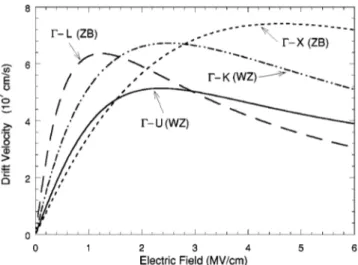
point. For the scattering timein Eq. 共2兲, we use the value given by the maximum scattering rate in each direction. Fig-ure 4 shows the corresponding drift velocity estimations rel-evant to high fields for both crystal phases. Different
low-field mobilities in Fig. 4, contrary to reality, are caused by using the maximum scattering rate throughout the band, even though this rate shows an isotropic character close to the CB edge 共cf. Fig. 1兲. The ⌫ – L direction of ZB GaN has the lowest onset field of 1 MV/cm for the observation of nega-tive differential conductivity共NDC兲, however, note the sen-sitivity of the onset field to angular variations 共cf. Fig. 4兲. There have already been several predictions of NDC in GaN 共Refs. 9–12兲 at field levels of around 150 kV/cm, all being based on the transfer of electrons to upper valleys, whereas, the NDC that we refer to here is caused by those carriers reaching the negative effective mass part of the band struc-ture at high fields before undergoing a scattering event, an idea initially proposed by Kro¨mer.13Recently, the possibility of NDC based on this mechanism was advocated14for cubic GaN beyond a field of ⬃50 kV/cm. This onset voltage is about 20 times lower than our estimate. Recent Monte Carlo investigations15along this line did not encounter any drastic change up to fields ⬃0.5 MV/cm with respect to a variation of the energy of the X valley, which further contradicts this previous prediction.14
In summary, to aid the high-field characterization of GaN, we present a full-band POP scattering analysis of CB electrons, comparing the ZB and WZ crystal phases. In gen-eral, the scattering rates in the ZB phase are lower than the WZ phase due to the lower density of states in the former. This suggests a possibility to have enhanced high-field mo-bility in ZB GaN in comparison with WZ GaN. High-field transport along the⌫ – L direction of ZB GaN characterized by a scattering time of 11 fs has the lowest scattering rate, as the POP emission to the L point is energetically not possible. The observation of NDC driven by the negative effective mass part of the band structure is predicted beyond a field of roughly 1 MV/cm for the ZB phase, and 2.3 MV/cm for the WZ phase.
This work is supported by ONR共Contract No. N00014-99-1-0014兲 and EPSRC 共Contract No. GR/L/56725兲.
1J. W. Orton and C. T. Foxon, Rep. Prog. Phys. 61, 1共1998兲. 2
A. Garcı´a and M. L. Cohen, Phys. Rev. B 47, 4215 共1993兲; 47, 4221 共1993兲.
3C. Bulutay, B. K. Ridley, and N. A. Zakhleniuk, Phys. Rev. B共in press兲. 4R. Wang, P. P. Ruden, J. Kolnik, I. Og˘uzman, and K. F. Brennan, J. Phys.
Chem. Solids 58, 913共1997兲.
5
G. Lehmann and M. Taut, Phys. Status Solidi B 54, 469共1972兲.
6M. R. Salehpour and S. Satpathy, Phys. Rev. B 41, 3048共1990兲. 7M. Farahmand and K. F. Brennan, IEEE Trans. Electron Devices 47, 493
共2000兲.
8
L. Esaki and R. Tsu, IBM J. Res. Dev. 14, 61共1970兲.
9B. Gelmont, K. Kim, and M. Shur, J. Appl. Phys. 74, 1818共1993兲. 10N. S. Mansour, K. W. Kim, and M. A. Littejohn, J. Appl. Phys. 77, 2834
共1995兲.
11
J. Kolnı´k, I˙. H. Og˘uzman, K. F. Brennan, R. Wang, P. P. Ruden, and Y. Wang, J. Appl. Phys. 78, 1033共1995兲.
12B. E. Foutz, S. K. O’Leary, M. S. Shur, and L. F. Eastman, J. Appl. Phys. 85, 7727共1999兲.
13H. Kro¨mer, Phys. Rev. 109, 1856共1958兲. 14
S. Krishnamurthy, M. van Schilfgaarde, A. Sher, and A.-B. Chen, Appl. Phys. Lett. 71, 1999共1997兲.
15K. F. Brennan共private communication兲.
FIG. 4. Comparison of drift velocity vs electric field for the ZB and WZ phases along several directions.
2709 Appl. Phys. Lett., Vol. 77, No. 17, 23 October 2000 Bulutay, Ridley, and Zakhleniuk