DIODE PROPERTY OF n-ZnO/p-Si HETEROJUNCTION STRUCTURE IN THE DARK AND ILLUMINATION CONDITION
Serap YİĞİT GEZGİN1, Abdullah KEPCEOĞLU1, Ahmet TOPRAK2, Yasemin
GÜNDOĞDU1, Hamdi Şükür KILIÇ1 ,3
1University of Selçuk, Faculty of Science, Department of Physics, Konya TURKEY 2Selçuk University, Bozkır Vocational School, Department of Electric and Energy,
Konya TURKEY
3University of Selçuk, Directorate of High Technology Research and Application
Center, Konya TURKEY Abstract
In this study, Zinc Oxide (ZnO) thin film was deposited on the Silicon (Si) wafer by Pulsed Laser Deposition (PLD) to form n-ZnO/p-Si heterojunction. The morphological and the crystal structure of ZnO thin film was analysed and interpreted by Atomic Force Microscopy (AFM) and X-Ray Diffraction (XRD), respectively. The absorption spectrum was obtained by using the UV-Vis spectra and the band gap (Eg) was
found by using Tauc Law. The current density-Voltage (J-V) plot was obtained at room temperature (RT) in the dark and under illumination. The barrier height (BH) and ideality factor were found about 0.46 eV and 1.35, respectively. The largest values of open circuit voltage (Voc) and short-circuit current (Jsc) were about 100 mV and 3×10⁻² mA/cm2,
respectively. It has been measured that ZnO/Si heterojunction diode behaves a solar cell like device under the illumination conditions.
Keywords: Heterojunction, open circuit voltage, short circuit current, barrier height, ideality factor
KARANLIK ve AYDINLIK ŞARTLARDA n-ZnO/p-Si HETEROEKLEM YAPISININ DİYOT ÖZELLİĞİ
Özet
Bu çalışmada, n-ZnO/p-Si heteroeklem oluşturmak için Silikon (Si) wafer üzerine Çinko Oksit (ZnO) ince film Puls Lazer Deposizasyon (PLD) ile depozit edilmiştir. ZnO ince filmin morfolojik ve kristal yapısı, sırasıyla Atomik Kuvvet Mikroskopu (AFM) ve
X-Ray Kırınımı (XRD) ile analiz edilmiş ve yorumlanmıştır. Soğurma spektrumu UV-Vis spektrumu kullanılarak elde edilmiş ve bant aralığı (Eg) Tauc yasası kullanılarak
bulunmuştur. Akım yoğunluğu-Gerilim (J-V) grafiği, oda sıcaklığında (RT) karanlıkta ortamda ve ışık altında elde edilmiştir. Bariyer yüksekliği (BH) ve idealite faktörü sırasıyla yaklaşık 0.46 eV ve 1.35 bulunmuştur. Açık devre voltajının (Voc) ve kısa devre
akım yoğunluğunun (Jsc) en büyük değerleri sırasıyla 100 mV ve 3x10⁻² mA/cm2’dir.
ZnO/Si heteroeklem diyotunun ışık altında güneş piline benzer bir cihaz gibi davrandığı gözlemlenmiştir.
Anahtar Kelimeler: Heteroeklem, açık devre voltajı, kısa devre akımı, bariyer yüksekliği, idealite faktörü
1. Introduction
Transparent Conductive Oxide (TCO) semiconductor thin films have presented some excellent properties such as simple processing steps, excellent blue response and low processing temperature to form p-n heterojunction diodes with a single crystalline silicon wafer structures [1]. ZnO semiconductor material has been used as a TCO material which has some important and unique properties such as wide direct band gap (3.37 eV), large exciton binding energy (60 meV), non-toxicity [2], good electrical conductivity, transparency, low cost of production, high thermal and mechanical stabilities and find a wide application area in electronics and optoelectronics. ZnO thin film exhibiting significant n-type conductivity without any doping process is transparent in the visible region of the spectrum [3], used in sensor technology, photodetectors, multiple quantum well structures [4], light emitting diodes, p-n heterojunction diodes [5, 6], solar cells, piezoelectric devices [7], flat-panel displays [8] and thin film transistors [9]. The single crystal Si material, which is used in n-ZnO/p-Si heterojunction structure has a natural abundance and easy to process, is one of an ideal quality substrate for high-quality ZnO thin film growth [10, 11].
Several methods, such as molecular beam epitaxy (MBE), magnetron sputtering, sol-gel process, metal organic chemical vapor deposition (MOCVD) and pulsed laser deposition (PLD), are used in the production of ZnO thin film [12]. PLD is a powerful and versatile technique having several advantageous for the easy production of ZnO thin film at relatively low cost production process and low process temperature. The thin films
can be produced in crystal, epitaxial and stoichiometric structure at low substrate temperature by PLD technique [13-20]. Therefore, PLD technique has many distinguishing features to produce high-quality ZnO thin film on Si wafer substrate [2]. In this study, we have produced a n-ZnO/p-Si heterojunction diode by PLD technique. The morphology and crystal structure of ZnO thin films were investigated by Atomic Force Microscopy (AFM) and X-Ray Diffraction (XRD), respectively. Its absorption spectrum was obtained by using a UV-vis spectrometer. The current density-voltage (J-V) plot was measured at room temperature (RT) in the dark and under illumination conditions. The solar cell behaviour of n-ZnO/p-Si heterojunction diode was investigated and interpreted in the following sections.
2. Experimental
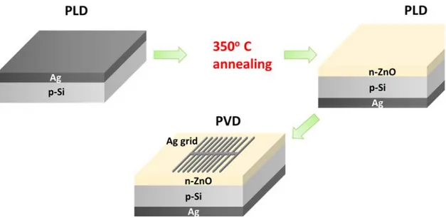
ZnO thin film as an n-type layer and Ag thin film back contact in Ag/ZnO/Si/Ag heterojunction structure were grown by PLD technique. Pulsed laser beam was used at 1064 nm wavelength with 40 mJ laser energy per pulse and 5 ns width at a 10 Hz repetition rate. The biconvex lens having a focal length of 50 cm was used to focus the laser beam onto the target material. The distance between the target and substrate was set to 50 mm. Before the experiment started, the vacuum chamber was evacuated down to 1×10⁻⁶ mbar. The p-type Si wafer (at (110) crystal orientation) was used as an active
layer in 500 μm thickness and 1.44 cm2 area.
Ag thin film was deposited on the back side of Si (110) wafer at RT for two hours, it was annealed at 350 oC for 5 minutes and then the ohmic contact was formed. Later,
O2 gas was let in to the vacuum chamber up to a pressure of 1.3 × 10⁻¹ mbar. ZnO thin
film was grown on the front side of Si wafer at RT for 95 minutes. The mask was placed on the thin film produced and the Ag thin film fingers were grown on ZnO thin film at RT as a front contact by applying Physical Vapor Deposition (PVD) technique (Figure 1).
3. Results and Discussion
3.1. Structure and optical properties of ZnO thin film
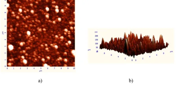
According to AFM image in Figure 2a, ZnO thin film consists of small particles has non-homogeneous distribution and density. The roughness value is about 19 nm (Figure 2b.) and, therefore, it does not show high porosity and it is close to the compact structure.
a) b)
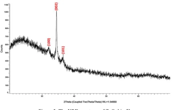
Figure 2. a) AFM (10μm×10μm area) and b) roughness images of ZnO thin film The XRD spectrum of ZnO thin film is given in Figure 3. ZnO thin film grown at RT which has a main peak at (002) orientation and peaks at (100), (101) orientations.
The fact that the ZnO thin film is in polycrystalline structure indicates that there are defects in the crystal structure, but the predominance of (002) peak shows that thin film is close to the quality ZnO structure [2, 7]. In addition, ZnO thin film growth in crystal structure at room temperature by the PLD system that affects the performance of the diode structure positively.
Figure 3. The XRD spectrum of ZnO thin film
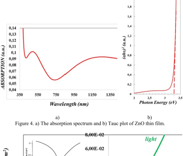
According to the absorption spectrum in Figure 4, the ZnO thin film is transparent to the visible region between 500 and 700 nm, while the IR region is absorbed. The high electron carrier concentration causes the absorption of electromagnetic radiation in visible region between 450-500 nm and the infrared portions of the spectrum (materials are considered to be n-type) [21].
The band gap energy (Eg) of ZnO thin film was defined by Tauc law in equation
(1):
(1) where, is constant, is the photon energy, is the band gap value. The linear portion of versus in the plot that gives as seen Figure 4b. of ZnO thin film was determined about 3,3 eV which is in good agreement with literature works [2, 22] and at this point, ZnO thin film has transparent conductive oxide (TCO) semi-conductor optical properties.
3.2. Current density-voltage characteristics of Ag/n-ZnO/p-Si/Ag
Figure 5 shows the current density-voltage (J-V) characteristics of Ag/n-ZnO/p-Si/Ag structure presented in the dark and under the illumination at RT. It is shown that the semi-logarithmic forward bias J–V characteristics under the illumination in the inset in Figure 5.
a) b) Figure 4. a) The absorption spectrum and b) Tauc plot of ZnO thin film.
Figure 5. J-V graphic of n-ZnO/p-Si heterojunction in the dark and under the illumination
According to J-V plot, it is observed that n-ZnO/p-Si diode show some rectifying behaviour but not an ideal rectifying behaviour [23]. This behaviour of ZnO/Si heterojunction can be analysed by the expression [24] in equation (2):
1
(2)where is the saturation current density, is the electronic charge, is the applied voltage, is ideality factor, is Boltzman’s constant and is the temperature in K. The saturation current density can be written by following expression [25],
∗ /
(3)
where A* is theoretical Richardson constant and 32 A/cm2K2 for ZnO, is barrierheight. The value of is determined to be 2.5×10⁻² mA/cm2 from straight line of
curve to 0. , the ideality factor can be defined by,
(4)
The ideality factor was calculated to be 1.35. If n is between 1 and 2, the tunnelling current occurs in the depletion region. Barrier height can be written by equation (5)
∗
(5) where , is the contact area. , the barrier height is calculated to be 0.46 eV. The ideal barrier height of ZnO/Si diode (the difference between the work functions of Si (4.97 eV) and ZnO (4.25 eV)) is about 0.72 eV [4]. But, barrier height in 0.46 eV that is lower than this value.
It can be emphasized that the n-ZnO/p-Si heterojunction structure is a non-ideal diode if the height of the barrier is low and the ideality factor is greater than 1. This may have been caused by a number of circumstances: the thickness of the SiOx layer formed
at the interface during the deposition or annealing processes, the tunnelling mechanism, the formed defects depending on oxygen vacancies in the crystal structure of ZnO thin film, the morphological disorders in the ZnO thin film and the low shunt resistance in the thin film, the lattice mismatch between ZnO thin film and Si wafer [7, 26].
3.3. The photoelectric property of Ag/n-ZnO/p-Si/Ag heterojunction
The forward current underthe 70 mW/cm2 power density illumination conditions
circuit voltage (Voc) and fill factor (FF) are given to be 3×10⁻² mA/cm2, 100 mV and 0.20,
respectively. In the forward bias region, the current in the dark exponentially increases in a very weak ratio while the current in the reverse bias region is almost negligible. However, in the illumination conditions, it has been measured that the Ag/n-ZnO/p-Si/Ag heterojunction structure exhibits the solar cell characteristics. According to J-V plot, forward current increases as the bias voltage under illumination increases. Furthermore, since the energy of the incident photon is greater than the band gap of ZnO and Si, the increase in the reverse bias current is observed [27]. If the charge carriers in the p-type Si was excited by the incident light, the photo-excited electrons were accumulated in the depletion area [28] and the photocurrent occur. However, n-ZnO/p-Si structure has very
little power conversion efficiency. There may be a few cases of low efficiency: the
above-mentioned situations which cause a low barrier height and a high ideal factor of 1, thick p-type Si active layer, the tunnelling mechanism, a polycrystalline structure of ZnO thin film. Because the active layer is very much thick (500 μm), the lifetime of the
photo-excited charge carriers is too low to reach the sides of the active layer and unfavourable recombination may occurs. Thus, photocurrent remains low and therefore the conversion efficiency remains low too. The undesirable charge transitions in the depletion region may occur depending on the SiOx layer or the morphological disturbances (pinholes, grain
boundaries, low shunt resistivity) of ZnO thin film at the interface. Thus, recombination, occurs in the depletion region, is the source of the lower conversion efficiencies. The ZnO thin film has a polycrystalline structure and an indication of grain growth in different directions. This situation can adversely affect the density and mobility of the charge
carriers on the film and hence the power conversion efficiency.
4. Conclusions
In this study, we produced Ag/ZnO/Si/Ag heterojunction structure. ZnO thin film produced in this work is transparent over a spectral range of 500-700 nm in the visible region, has relatively high absorbance in the IR region and has ~3.3 eV band gap value. ZnO thin film is ideal for TCO material with these optical properties. Furthermore, it has a polycrystal structure and (002) main peak is dominant. J-V plot of ZnO/Si heterojunction diode was obtained under the illumination condition (70 mW/cm2) and in
but, exhibits rectifying behaviour under the illumination. Under the illumination, barrier height and ideality factor are given to be 0.46 eV and 1.35, respectively. In addition, Ag/ZnO/Si/Ag structure exhibits the solar cell behaviour with open circuit voltage of 100 mV, short circuit current density of 3×10⁻² mA/cm2, fill factor of 0,20 and the relatively
low power conversion efficiency is due to the photo current caused by photo-excited charge carriers in the Si active layer. The interface situations in ZnO/Si heterojunction, tunnelling mechanism, thick Si active layer, the polycrystal structure of ZnO thin film, pinholes and grain boundaries in the ZnO film which can cause the lower efficiency. Acknowledgements
Authors kindly would like to thank,
- Scientific and Technical Research Council of Turkey (TUBITAK) for financial support via Grant No. 1649B031503748,
- Scientific Research Projects Coordination Unit of Selçuk University for financial support via Projects Nos. 14401087, 13301022 and
- Selçuk University, High Technology Research and Application Center for supplying with Infrastructure.
The data presented in this work will be as a part of the Ph.D. thesis of the Serap YİĞİT GEZGİN.
References
[1] L. Shen, Z. Ma, C. Shen, F. Li, B. He, and F. Xu, "Studies on fabrication and
characterization of a ZnO/p-Si-based solar cell," Superlattices and
microstructures, vol. 48, no. 4, pp. 426-433, 2010.
[2] S. Chirakkara and S. Krupanidhi, "Study of n-ZnO/p-Si (100) thin film heterojunctions by pulsed laser deposition without buffer layer," Thin Solid Films, vol. 520, no. 18, pp. 5894-5899, 2012.
[3] M. Jayaraj, "Electrical Characteristics of n-ZnO/p-Si Heterojunction Diodes Grown by Pulsed Laser Deposition at Different Oxygen Pressures," 2007.
[4] P. Misra, T. Sharma, S. Porwal, and L. Kukreja, "Room temperature photoluminescence from ZnO quantum wells grown on (0001) sapphire using
buffer assisted pulsed laser deposition," Applied physics letters, vol. 89, no. 16, p. 161912, 2006.
[5] R. Hoffman, J. Wager, M. Jayaraj, and J. Tate, "Electrical characterization of transparent p–i–n heterojunction diodes," Journal of Applied Physics, vol. 90, no. 11, pp. 5763-5767, 2001.
[6] H. Ohta, M. Orita, M. Hirano, and H. Hosono, "Fabrication and characterization of ultraviolet-emitting diodes composed of transparent pn heterojunction, p-SrCu 2 O 2 and n-ZnO," Journal of Applied Physics, vol. 89, no. 10, pp. 5720-5725, 2001.
[7] S. Sharma and C. Periasamy, "Simulation study and performance analysis of n-ZnO/p-Si heterojunction photodetector," Journal of Electron Devices, vol. 19, no. 2014, pp. 1633-1636, 2014.
[8] C. Lee, T. Lee, S. Lyu, Y. Zhang, H. Ruh, and H. Lee, "Field emission from well-aligned zinc oxide nanowires grown at low temperature," Applied Physics Letters, vol. 81, no. 19, pp. 3648-3650, 2002.
[9] R. Hoffman, B. J. Norris, and J. Wager, "ZnO-based transparent thin-film transistors," Applied Physics Letters, vol. 82, no. 5, pp. 733-735, 2003.
[10] Y. Zhang, G. Du, B. Zhang, Y. Cui, H. Zhu, and Y. Chang, "Properties of ZnO thin films grown on Si substrates by MOCVD and ZnO/Si heterojunctions,"
Semiconductor science and technology, vol. 20, no. 11, p. 1132, 2005.
[11] S. Chand and R. Kumar, "Electrical characterization of Ni/n-ZnO/p-Si/Al heterostructure fabricated by pulsed laser deposition technique," Journal of Alloys
and Compounds, vol. 613, pp. 395-400, 2014.
[12] F. Yakuphanoglu, Y. Caglar, M. Caglar, and S. Ilican, "ZnO/p-Si heterojunction photodiode by sol–gel deposition of nanostructure n-ZnO film on p-Si substrate,"
Materials Science in Semiconductor Processing, vol. 13, no. 3, pp. 137-140, 2010.
[13] W. Marine, L. Patrone, B. Luk'yanchuk, and M. Sentis, "Strategy of nanocluster and nanostructure synthesis by conventional pulsed laser ablation," Applied
surface science, vol. 154, pp. 345-352, 2000.
[14] J. Alonso, R. Diamant, P. Castillo, M. Acosta–García, N. Batina, and E. Haro-Poniatowski, "Thin films of silver nanoparticles deposited in vacuum by pulsed
laser ablation using a YAG: Nd laser," Applied Surface Science, vol. 255, no. 9, pp. 4933-4937, 2009.
[15] J. Schou, "Physical aspects of the pulsed laser deposition technique: The stoichiometric transfer of material from target to film," (in English), Applied
Surface Science, vol. 255, no. 10, pp. 5191-5198, Mar 1 2009.
[16] H. El Ouazzani et al., "Novel styrylquinolinium dye thin films deposited by pulsed laser deposition for nonlinear optical applications," The Journal of Physical
Chemistry C, vol. 116, no. 12, pp. 7144-7152, 2012.
[17] H. Ş. Kılıç and H. Durmuş, "YENİ BİR PULS LASER DEPOZİSYON (PLD) SİSTEMİ TASARIMI, ÜRETİMİ VE UYGULAMALARI," Selçuk Teknik
Online Dergi, vol. 15, no. 1, pp. 24-43, 2016.
[18] A. Zawadzka, P. Płóciennik, Y. El Kouari, H. Bougharraf, and B. Sahraoui, "Linear and nonlinear optical properties of ZnO thin films deposited by pulsed laser deposition," Journal of Luminescence, vol. 169, pp. 483-491, 2016.
[19] S. Y. Gezgin, A. Kepceoglu, A. Toprak, and H. S. Kilic, "Investigation of Conversion Efficiency of n-ZnO/p-Si Heterojunction Device Produced by Pulsed Laser Deposition (PLD)," in International Congress on Semiconductor Materials
and Devices, Konya, 2017: Materials Today Proceedings.
[20] S. Y. Gezgin, A. Kepceoğlu, and H. Ş. Kılıç, "An experimental investigation of localised surface plasmon resonance (LSPR) for Cu nanoparticles depending as a function of laser pulse number in Pulsed Laser Deposition," AIP Conference
Proceedings, vol. 1815, no. 1, p. 030020, 2017.
[21] E. Premalal, N. Dematage, S. Kaneko, and A. Konno, "Preparation of high quality spray-deposited fluorine-doped tin oxide thin films using dilute di (n-butyl) tin (iv) diacetate precursor solutions," Thin Solid Films, vol. 520, no. 22, pp. 6813-6817, 2012.
[22] E. Keskenler et al., "Growth and characterization of Ag/n-ZnO/p-Si/Al heterojunction diode by sol–gel spin technique," Journal of Alloys and
Compounds, vol. 550, pp. 129-132, 2013.
[23] A. O. Mousa, "Fabrication and Characterization of ZnO/p-Si Heterojunction Solar Cell," World Scientific News, vol. 18, pp. 118-132, 2015.
[24] F. Yakuphanoglu, "Electrical characterization and device characterization of ZnO microring shaped films by sol–gel method," Journal of Alloys and Compounds, vol. 507, no. 1, pp. 184-189, 2010.
[25] F. Bedia, A. Bedia, and B. Benyoucef, "Electrical properties of ZnO/p-Si heterojunction for solar cell application," International Journal of Materials
Engineering, vol. 3, no. 4, pp. 59-65, 2013.
[26] N. Al-Hardan, M. A. Hamid, N. M. Ahmed, R. Shamsudin, and N. K. Othman, "Ag/ZnO/p-Si/Ag heterojunction and their optoelectronic characteristics under different UV wavelength illumination," Sensors and Actuators A: Physical, vol. 242, pp. 50-57, 2016.
[27] A. A. Yousif, "Current transport studies of n-ZnO/p-Si hetero-nanostructures grown by pulsed laser deposition," Int. J. Appl. Innov. Eng. Manag., vol. 3, 2014. [28] P. Hazra, S. Singh, and S. Jit, "Ultraviolet photodetection properties of ZnO/Si heterojunction diodes fabricated by ALD technique without using a buffer layer,"
JSTS: Journal of Semiconductor Technology and Science, vol. 14, no. 1, pp.