T ifè
I3S6
CHÄfv.cTEBSATtcK
о ?гит т ю
crystals
at
MiCñOVYAVS FRSGUSnaSS
Cl t г ’-> í' -i ‘ o ■ ... .VÏ · •fe -■ V e § ^ T L il : Ï íí> ' Г ‘‘ 0 í r 4 I- ЧU4I·. . , .· Λ /» .чи· .■ i 'Cs A.«'·' ' H ; ' ’ À ^ / ѵ ■ 'tlf ^ ■■ .-.J' V v,.~ ;.í^ ■ -;;;· - ' І з і - Г . / ■ r í ' . ?·■ ' 2 ^jVA, ;... C \ Î t 'i ¿u b:-' ■ îCt' ■' V '(’ ; J! - " í A - b í T f ' t ô A í < í L,t.- f ■·.. ' f · · ; ^••· Л /П í ;■. / T--VT*;/ ?·*’·· ! ? ·}ι w w t : í 'c T e r n a fk u r a n >?»4 ■ - " í ! “ í c H · .·> .',' 4 Q . ü t A . ti 1. 1' i, W - w '<b>CHARACTERIZATION OF PHOTONIC CRYSTALS AT
MICROWAVE FREQUENCIES
A THESIS
SUBMITTED TO THE DEPARTMENT OF PHYSICS AND THE INSTITUTE OF ENGINEERING AND SCIENCE
OF BILKENT UNIVERSITY
IN PARTIAL FULFILLMENT OF THE REQUIREMENTS FOR THE DEGREE OF
MASTER OF SCIENCE
By
Burak Temelkuran
September 1996
B.035237
&İCъ г п
■ P u n т ц 13? 4I certify that I have read this thesis and that in my opinion it is fully adequate, in scope and in quality, as a dissertation for the degree of Master of Science.
____________
Asst. Prof. Ekmel (Supervisor)
I certify that I have read this thesis and that in my opinion it is fully adequate, in scope and in quality, as a dissertation for the degree of Master of Science.
Prof. Alexander Sixuna^vsky
I certify that I have read this thesis and that in my opinion it is fully adequate, in scope and in quality, as a dissertation for the degree of Master of Science.
Approved for the Institute of Engineering and Science:
Prof. Mehmet Bara
Abstract
CH ARACTERIZATION OF PHOTONIC CRYSTALS AT
MICROWAVE FREQUENCIES
Burak Temelkuran
M. S. in Physics
Supervisor: Asst. Prof. Ekmel Ozbay
September 1996
VVe investigated the surface reflection properties of layer-by-layer photonic crystals, for dielectric and metallic based photonic crystals. By using a Fabry- Perot cavity analogy with the reflection-phase information of the photonic crystals, we predicted defect frequencies of planar defect structures. Our predictions were in good agreement with the measured defect frequencies. The Fabry-Perot cavity analogy was also used to relate the quality factors of the planar defect structures to the transmission of the mirrors of the cavity. A simple model was used to simulate the transmission spectra of planar defect structures, which agreed well with the experimental data. We also investigated the transmission and reflection properties of two different metallic crystal structures (face-centered- tetragonal and simple tetragonal). We obtained rejection rates of 7-8 dB per layer from metallic crystals. Defect modes created by removing rods resulted in high peak transmission (80%), and high quality factors (1740). Our measurements were in good agreement with theoretical simulations of metallic structures. Planar defect structures built around metallic structures resulted in higher quality factors (2250). We observed high reflection-rejection ratios (-80 dB) at defect frequencies
for planar defect structures, which was explained by using the Fabry-Perot analogy. Finally, the enhanced field inside the defect volume was measured, by using a monopole receiver antenna inserted inside the defect. The maximum observed enhancement with respect to the incident field was around 200 for a planar defect structure. By placing a Schottky diode detector inside planar and box-like defects, we built resonant cavity enhanced (RCE) detectors and measured the enhanced field inside the defect.
K e y w o r d s : Photonic Crystals, Fabry-Perot Cavity, Planar Defects, Lo calized Defects, Quality Factor, Optical Field Enhancement, Schottky Diode Detector, Metallic Photonic Crystal, Resonant Detector, Reflection-Phase Measurement.
ö z e t
m i k r o d a l g a
FREKANSLARINDA FOTONİK
KRİSTALLERİN K A R A K T E R İZA SY O N U
Burak Temelkuran
Fizik Yüksek Lisans
Tez Yöneticisi: Asst. Prof. Ekmel Özbay
Eylül 1996
Katmanlardan oluşan fotonik kristallerin yüzey yansıtma özelliklerini, dielek- trik ve metal kristaller için inceledik. Fabry-Perot çınlaç benzeşimini fotonik kristallerin yansıtma-fazı bilgisi ile birlikte kullanarak, düzlemsel düzensizlik yapılarının rezonans frekanslarını tahmin ettik. Kuramsal tahminlerimiz, ölçülen rezonans frekanslarına uyuyordu. Fabry-Perot çınlaç benzeşimi, düzlemsel düzensizlik yapılarının kalite faktörleriyle çmlacm aynalarının geçirgenliği arasında bir ilişki kurmak için de kullanıldı. Düzlemsel düzensizlik yapılarının geçirgenlik spektrumunu simüle etmek için, sonuçları deneysel verilerle u}mşan basit bir model kullanıldı, iki ayrı metalik kristal yapısının (basit tetragonal ve yüz- rnerkezli-tetragonal) geçirgenlik ve yansıtma özellikleri incelendi. Metalik kristallerden katman başına 7-8 dB sinyal düşüşleri elde edildi. Çubukların çıkarılması ile oluşturulan rezonans modları, yüksek değerde tepe geçirgenliği (%80) ve yüksek kalite faktörleri (1740) ile sonuçlandı. Olçünîlerimiz ile metalik yapıların kuramsal simülasyonları birbirini tutuyordu. Metalik yapılarda oluşturulan düzlemsel düzensizliklerin kalite faktörleri daha \diksekti (2250). Bunun yanında, düzlemsel düzensizliklerin rezonans frekanslarında yüksek
oranlarda yansıtma-reddi gözlendi (-80 dB), ve bu olay Fabry-Perot benzeşimi ile açıklandı. Son olarak, tek kutupsal bir anten alıcı olarak kullanılarak, düzensizliğin içinde kuvvetlendirilmiş alan ölçümleri yapıldı. Gözlemlenen en büyük kazanç, sinyalin, gönderilen sinyale göre yaklaşık 200 kat kadar artmasıydı. Düzlemsel ve kutu benzeri düzensizliklerin içine Schottky diyot algılayıcıları yerleştirilerek, resonans çmlaç ile kuvvetlendirilmiş bir algılayıcı yapıldı ve düzensizlik içerisindeki kuvvetlendirilmiş alan ölçüldü.
Anahtar
sözcükler: Fotonik Kristaller, Fabry-Perot Çmlacı, Kristal Düzensizliği, Kalite Faktörü, Optik Alan Kazancı, Schotky Diyot Detektör, Metalik Fotonik Kristaller, Rezonans Algılayıcı, Yansıtma-Faz Ölçümleri.
Acknowledgement
I would like to express my gratitude to my thesis supervisor Prof. Ekmel Ozbay for his invaluable guidance and motivation during my graduate study. I’d also like to thank Prof. M. Sigalas and Prof. K.M. Ho from ISU, for helping me with their simulations. I am also grateful to the members of the Department of Physics, Bilkent University, for valuable discussions and comments. I also thank all of my friends, who supplied me continuous morale support, and especially Canan, who decided to spend all her life with me.
Contents
Abstract i
Özet iii
Acknowledgement v
Contents vi
List of Figures viii
1 Introduction 1
1.1 M otivation ... 2 1.2 H istory... 4 1.3 Defect Structures and D o p i n g ... 6
1.4 Antennas 9
1.5 W a v e g u id e s ... 11 1.6 Metallic photonic crystals and other applications... 12
1.7 Summary of this work 12
2 Reflection Properties and Defect Formation 14
2.1 Defect s t r u c tu r e s ... 14 2.2 Reflection m easurem ents... 17
2.3 Fabry-Perot analogy 18
2.4 Quality F a ctor... 23
3 Metallic Photonic Crystals 27
3.1 Structure ... 27
3.2 Transmission properties 29
3.3 Defect s t r u c tu r e s ... 32 3.4 Reflection properties and Fabry-Perot type cavities in metallic
s t r u c tu r e s ... 41
4 Resonant Detectors Inside Dielectric Photonic Crystals 46
4.1 The circulating intensity m a g n ifica tio n ... 47 4.2 Experimental s e t u p ... 50 4.3 M easurem ents... 52
5 Conclusions 59
List of Figures
1.1 Inhibition of spontaneous emission... 3
1.2 The drilling technique used in the construction of the first photonic crystal that possessed 3-D P E G ... 5
1.3 Layer-by-layer s t r u c t u r e ... 7
1.4 Sample defect transmission characteristics... 8
1.5 Antenna a pp lication s... 10
1.6 Waveguide carved inside a 1-D photonic crystal... 11
2.1 Experimental s e t u p ... 15
2.2 Reflection and transmission ch aracteristics... 16
2.3 Transmission from a single rod removed defect structure 16 2.4 Phase inform ation... 17
2.5 High Q factor defect mode... 19
2.6 Phase com parison... 21
2.7 Double d e f e c t ... 22
2.8 Inverse Q factor and Transmission... 24
2.9 Comparison of defect theory with experiment 25 3.1 Two types of layer-by-layer photonic cry sta ls... 28
3.2 The transmission characteristics of fct and st metallic structures . 30 3.3 Transmission from 10-layer metallic photonic crysta l... 31
3.4 Transmission at different angle of incidences... 32
3.5 Comparison of the transmission characteristics of defect structures of st and fct crystals... 33
3.6 Transmission Characteristics of an st 18-Layer Defect... 35
3.7 Comparison of Theoretical and Experimental results of a Defect
M o d e ... 36
3.8 Defect mode with a high Q-factor... 37
3.9 Comparison of experimental peak amplitudes of defect modes with the th e o ry ... 38
3.10 The additional peaks observed for the planar defect structure. 40 3.11 Reflection and transmission characteristics of st c r y s t a l ... 41
3.12 The reflection-phase information... 42
3.13 Phase Comparison of Theory and Experiment (1 )... 43
3.14 Phase Comparison of Theory and Experiment (2 )... 43
3.15 High reflection rejection from a defect structure... 45
4.1 Magnification of the circulating signal. 48 4.2 Fabry-Perot m odeling... 49
4.3 RCE m odeling... 50
4.4 Experimental s e t u p ... 51
4.5 Defect Structure... 52
4.6 Transmission spectra of a defect mode 53 4.7 Power enhancement of a defect m o d e ... 54
4.8 Enhancement of the field inside a planar defect... 55
4.9 Transmission spectra from a box-like c a v i t y . ... 56
4.10 Circulating intensity magnification inside a box like cavity (1). . . 56
4.11 Circulating intensity magnification inside a box like cavity (2). . . 57
Chapter 1
Introduction
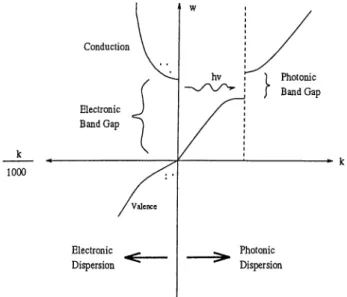
Electrons in a crystal have energy bands that are separated by forbidden regions, which are called electronic band gaps. In these regions, wavelike electron orbitals are not allowed. The basic reason behind the band structure, is the periodicity of the potential within the crystal. On the other hand, for photons, a material with a periodically changing dielectric constant may also result in a similar band structure. Using this analogy, the first photonic band gap (PBG ) crystal was proposed by Eli Yablonovitch in 1987.^ The main goal is to have a frequency band in which the propagation of the electromagnetic waves are forbidden for every direction. So what we call a photonic crystal is a periodically arranged structure, where air or dielectric material has lattice-like behavior. Such a PBG crystal reflects the propagating electromagnetic (EM) waves in all directions due to Bragg-scattering conditions. We can easily see this analogy in the equations of a propagating electron wave in a space-variant potential U (r) (1.1), and the propagation of EM waves in a dielectric media with a space-variant dielectric function for the electric field amplitude E (r) (1.2).^
.
+ l/(r)| 4(r) = £ « (r )
UJ to
- V ^ - - - e y /„ e i ( r ) E (r) + V (V · E (r)) = cq— E (r)
(
1
.
1
)
In equation 1.1, h is the Planck constant divided by 2ir, rrC is the effective electron mass, and ’P(r) is the scalar wave function. In the second equation, cu is the angular frequency of the field, and c is the speed of light in free space. Except the term V ( V · E ), the anology between the Schrödinger equation (1.1) and the Maxwell equation (1.2) is obvious. The total dielectric constant in the second equation is separated as e(r) = Cq + e/iuci(r), into its average value cq and
a spatially fluctuating part e/;„ci(r). The latter plays a role analogous to the K(r) in the Schrödinger equation, and the quantity plays the role of the energy eigenvalue E of the Schrödinger equation.
The PBG idea has led to proposals for many novel applications at optical wavelengths, such as thresholdless lasers^ and efficient single mode light emitting diodes.^’® These applications are later extended to microwave and millimeter wave regime, such as efficient reflectors, millimeter wave antennas. Alters, sources, and
w a v e g u id e s .
9
g, result, there have been a great deal of interest in this research subject during the last few years.1.1
Motivation
Chapter 1. Introduction 2
The control of spontaneous emission plays an important role in many applications based on quantum electronics and quantum optics. Many corresponding examples can be found. The threshold of a laser, the current gain in heterojunction bipolar transistors, and the maximum available output voltage in solar cells, all depend on the spontaneous recombination of electrons and holes.
Before 1980’s, spontaneous emission was known to be a natural phenomena which could not be controlled. Later, it was found that spontaneous emission could be reduced inside a metallic waveguide, where no propagation mode is allowed up to a certain cut-off frequency.^^ But as metals absorb most of the EM waves at optical frequencies, this method is not feasible at optical wavelengths. On the other hand, dielectric materials or insulators may be used to overcome this absorption problem. So dielectric based photonic crystals which do not allow propagation of EM waves can also be used to inhibit spontaneous emission.
Figure 1.1 shows how the spontaneous emission can be controlled by a photonic c r y s t a l . I n a semiconductor, a photon is emitted by the recombination of an electron in the valence band with a hole in the conduction band. However, if the photonic crystal is designed to have a band gap covering the frequency of the emission, the photon will have no mode to couple, and the recombination will simply be inhibited.
Chapter 1. Introduction 3
F igu re 1.1: Inhibition of spontaneous emission.
Right side, the dispersion relation for the EM waves, left side, the dispersion relation for electron waves of a typical direct-gap semiconductor.
An example can clarify the use of this idea. Yamamoto was able to limit the noise in an electrical current flow by a good quality metal film resistor, and drived a high-quantum efficiency-laser diode with this r e s i s t o r . A s s u m i n g a 100% efficient laser, a single photon would be produced for every single electron. With this design, a photon could be used as a single communication unit. However the problem was to achieve such a highly efficient laser. If the typical amount of random spontaneous emission captured by the cavity of the laser were to be around 50%, then the signal to noise ratio (SNR) would only be 3 dB. This SNR is quite low, and should be increased. Using a photonic crystal, spontaneous emission could be reduced to 1%. That would correspond to a 20 dB SNR, which
is a highly desirable value.
It should be noted that the idea of PBG is different from the concept of one-dimensional stop bands used in electrical engineering. Rather, the photonic crystals are expected to have stop bands in all directions. Early studies made on X-ray diifractions from natural fee crystals showed narrow stop b a n d s . T h i s idea acted as the basis in the development of the PBG theories. But due to the refractive-index difference between vacuum and matter being low, the stop bands that are observed were narrow. Calculations showed that with refractive-index difference higher than 2, these stop bands may be opened to cover all directions in reciprocal space.^^
Chapter 1. Introduction 4
1.2
History
Photonic crystals which would be functional at optical frequencies require submicron dimensions. However, due to the difficulties in fabrication, people first tried to construct crystals at larger dimensions suitable for microwave characterization (15 GHz). The early PBG studies concentrated on testing various fee type fabricated crystals. The reason for choosing fee type crystals was their Brillouin zone being close to a sphere. Otherwise, the k vectors along different directions would differ in magnitude, and corresponding gaps would not overlap. In one of the early tries, fee type of periodicity for the spherical dielectric atoms was chosen,^ where the dielectric constant of these spherical atoms was 3.06. These were embedded inside a blue foam material of dielectric constant near unity. Another crystal was fabricated by Yablonovitch et al by drilling t e c h n i q u e s . I t was a spherical-void structure with oversized voids breaking through the walls of Wigner-Seitz (WS) unit cells. Although theories of that time predicted that the second crystal should possess a PBG in all directions, both crystals failed to produce a stop band. The reason behind this failure was the treatment of the EM field as a scalar field as in Schrodinger’s approach, which resulted in wrong predictions.
early structures did not have a full band gap due to band crossing along W direction of the Brillouin zone.^®’^® The problem of band crossing was solved by a diamond structure suggested by the Iowa State group of Ho et ald^ This predicted structure was later fabricated by drilling a solid dielectric material from three different angles, each 35.26° away from the normal and spread 120° on the a z i m u t h . T h e crystal in the end was a full 3-D fee structure with roughly cylindrical void atoms. This was the first experimental photonic crystal that possessed 3-D stop band. Along (111) direction, a gap extending from 13 GHz to 16 GHz was observed, with around 50 dB attenuation.
Chapter 1. Introduction 5
F ig u re 1.2: The drilling technique used in the construction of the first photonic crystal that possessed 3-D PBG.
After this verification of the existence of photonic crystals, there was an increased effort in this research area. Scientists searced for new structures that could be more easily fabricated, and could be scaled down to optical frequencies. A new crystal that meets these requirements was invented by the Iowa State g r o u p . T h e designed structure, which was called layer-by-layer photonic crystal, has 3-D PBG, and could also easily be scaled to lower dimensions. Each layer of crystal was formed by dielectric rods arranged parallel to each other separated
by a distance a. As seen in figure 1.3, each layer is stacked to the previous one by rotating the layer 90° with respect to the previous layer. Every third layer is parallel to the first one with a shift of a /2 in the direction perpendicular to the rods. The fourth layer is shifted the same way with respect to the second layer. So a unit cell of 4 layers of length c, where every fifth layer repeats the first one, is obtained. The angle between adjacent layers may vary from 90° to 60°. The structure has the symmetry of a face centered tetragonal (fct) type of structure. The crystal can be derived from a diamond structure if 110 chains of atoms were to be replaced by dielectric rods for the special case of c /a = \ /2 .
This structure is important in the sense that, its dimensions could easily be lowered. Using the anisotropic etching property of Si by KOH, the layers of these crystals were prepared by micromachining techniques at lower scales. First a gap around 100 GHz was r e a c h e d . T h e n the dimensions were further scaled down to achieve a photonic crystal with a full band gap around 500 GHz.^° By using special silicon thinning methods and double etching the wafers from both faces, this technique could be extended to have photonic band gaps around 3 THz.^^
Chapter 1. Introduction 6
1.3
Defect Structures and Doping
Similar to the doping of semiconductor crystals, localized electromagnetic modes can be produced in photonic crystals by introducing defects that break the symmetry of the c r y s t a l . T h i s can be achieved by two different methods. First, we can add extra dielectric material to the crystal, which acts like a donor atom in a semiconductor. Second, we can remove some part of the dielectric material from the crystal, which acts like an acceptor atom. Experiments show that the acceptor modes, acting like microresonator cavities, are of greater importance with their highly localized and single mode cavity c h a r a c t e r i s t i c s . T h e s e localized modes within the band gap are observed in previously mentioned photonic crystals. As an example, a defect structure can be produced by removing a part or all of a single rod from a single layer in a layer by layer structure. The transmission profile does not change from that of the core crystal. The only change is in the
Chapter 1. Introduction
F ig u re 1.3: Layer-by-layer structure
The design of an fct type of layer-by-layer crystal with a 3-D PEG. The structure is built by an orderly stacking of dielectric rods.
localized mode frequency, where a transmission peak appears inside the gap. The experimentally observed Q factors (quality factor, defined as the center frequency divided by the peak’s full width at half maximum) of these localized modes were around 1000-2000, while the theory expected to have high Q factors of the order of 10® for such defect structures.^® The finite size of the crystal and the material absorption were the main reasons for this significant difference.
Chapter 1. Introduction
F ig u re 1.4; (a) Transmission attenuation from a defect free photonic crystal, (b) Transmission spectra of a photonic crystal with a single acceptor in the middle, (c) Transmission spectra of a photonic crystal with a single donor defect, leading to two shallow donor modes.
With the introduction of localized modes, photonic crystals can be used in a variety of applications. The spontaneous emission was controlled by forbidding the propagation at a range of frequencies by the core crystal. By the introduction of a defect, a single frequency can be adjusted to allow stimulated emission. By this way, the coupling coefficient of spontaneous emission into stimulated emission could be increased from 10“ ® to approximately 1 in a semiconductor laser. This would mean thresholdless lasers, which are well worth fighting for.^ A similar approach can be used to achieve single mode light emitting diodes (SM-LED). The coupling coefficient of spontaneous emission to that of the desired single mode is very low in an SM-LED. The defect frequency of the photonic crystal can be arranged to match the single mode operating frequency of the diode. This would increase the coupling coefficient, up to unity.‘‘ ’®
These were the major motivations of the photonic crystals in the beginning. However, the possible applications in the area went far beyond the expectations.
Many applications came into view with the work done at microwave and millimeter wave frequencies. The most important ones are efficient antennas on photonic crystals and waveguide applications.
1.4
Antennas
Chapter 1. Introduction 9
Photonic crystals can also be implemented in the area of signal propagation and control. Antenna applications are good examples for this approach. In microwave and millimeter-wave integrated circuits, the control of the radiation from a dipole antenna is of great importance. In such circuits, the antenna is mounted on a semiconductor substrate, which enhances the performance and functionality of the circuit. But most of the power from the antenna on a dielectric substrate is radiated into the substrate. The ratio of the power radiated into the substrate, to the power radiated into air is where e is the dielectric constant of the substrate. As an example, a dipole antenna on a GaAs substrate emits 46 times more power into the substrate than into the air. Also the radiated waves, which have angle of incidence greater than the critical angle, are trapped inside the substrate due to total internal reflection (figure 1.5). Since this critical angle in GaAs is a small value, around 16°, a big percentage of the field is trapped. As a result, standard antennas on GaAs or Si radiate only 2-3% of their power into air. If a thin substrate is used to overcome the loss due to this trapping, another problem arises. A 180° phase shift comes from the reflection at the bottom conductor, resulting the radiation to cancel out at driving point. These problems can be solved, if the antenna was to be mounted on a 3-D photonic crystal, from which the radiation will fully be reflected in all directions. Since the reflections occur due to the Bragg scatterings, the phase shift of the reflected field won’t cancel out the radiated one. People use metallic feedhorns, which are more efficient than dielectric structures, at frequencies above 20 GHz. But the problem with these antennas is that the reflection occurs only on the surface of a metal. So all the power lost is converted to heat on the surface, causing overheating in a very small volume. Whereas in photonic crystals, the reflections
Chapter 1. Introduction 10
occur within at least a unit cell, which is much longer than the skin depth of the metals. As a result, the heat is disti'ibuted over a large volume, which would enable a lower operating temperature. Experiments done by mounting a dipole antenna on a photonic crystal shows that nearly all the field is radiated into air, which proves the usefullness of this idea.®’^’^^
(a)
Ait
I Trapped
r Radiation
(b)
Air
Photonic
Crystal
Antenna
Propagation of the Wave
Forbidden
Air
F igu re 1.5; Antenna applications
(a) Antenna mounted on a semiconductor substrate. Most of the power goes into the substrate, and also trapped inside the it. (b) Antenna on a photonic crystal. The crystal fuUy reflects the radiated field. The radiated field is directed and enhanced.
Chapter 1. Introduction 11
1.5
Waveguides
F ig u re 1.6: Theoretical simulation of a waveguide carved inside a 2-D photonic c r y s t a l . T h e light is guided through defects. The bright spots correspond to enhanced optical field.
Waveguides allow only certain electromagnetic wave modes to propagate inside the structure. There are many corresponding applications, which are of great importance in technology. As metals absorb most of the power at optical frequencies, dielectric-based waveguides are usually used at optical frequencies. These structures rely on the total internal reflection of the EM waves. However, there is a problem in guiding the wave through sharp edges, and tight curves. The angle of incidence would be too high for total internal reflection when the wave turns through a tight curve. So, most of the field would be radiated and lost. To change the direction of a wave with a dielectric guide, smooth curves which require long distances are needed. On the other hand, a waveguide can be carved through a photonic crystal, in which the guided modes can travel freely (figure 1.6). Therefore the trapped wave is guided without loss through the carved waveguide, even if it has tight c o r n e r s . T h i s would be helpful in lowering the size of integrated optical circuits.
Chapter 1. Introduction 12
1.6
Metallic photonic crystals and other
applications
Although metals are quite lossy at optical frequencies, they act as perfect conductors at microwave and millimeterwave frequencies. The initial interest for metals in PBG studies arised from the idea of obtaining high attenuation with fewer number of layers compared to the dielectric-based crystals. With a very low filling ratio and few number of layers, much lighter photonic crystals can also be achieved. The experiments show that the metallic photonic crystals have stop bands starting at zero frequency up to a cut-off frequency
This high-pass stopband is called as the metallicity gap. At higher frequencies, due to the periodicity of the structure, other stop bands are also observed. These are the band gaps, with lower and upper band edges, as in dielectric structures. Experiments on defect structures in metallic crystals also show similar localizations of electromagnetic w a v e s . H o w e v e r , the Q-factor of those defect modes are lower than those of the dielectric photonic crystals.
Beyond these, at microwave and millimeterwave frequencies, many other possible applications may be developed. A doped photonic crystal, in which the frequency of the localized mode is tuned to the desired frequency, may act as a bandpass filter. The frequency of this mode may be sensitive to temperature, or to the length of an object placed inside the crystal. So the photonic crystal may be used as a tunable sensor for temperature, length or any other such external parameter.
1.7
Summary of this work
Using the layer by layer photonic crystal, we first worked on the characteristics of simple defects. Then, we worked on the reflection and transmission characteristics of dielectric-based photonic crystals. We observed that the phase of the reflected waves had strong polarization dependence. The properties of the crystals with planar defects; which are analogous to Fabry-Perot resonators, were investigated.
Chapter 1. Introduction
13
Using the phase information of the reflected waves from the mirrors of the defect (or cavity), a simple method to predict the defect frequency was developed. The predicted frequencies were in good agreement with the experimental data. The theory was similar to that of Fabry-Perot resonators, where the localization of the wave occurred when phase shift in a round trip was a multiple of 2ir.
The transmission spectra of the walls of the cavity was compared with the Q- factors of the defect modes. The quality factor of the defect mode was inversely proportional to the transmitted power from the walls of the cavity. High Q factors, around 5000, were observed for the defect modes within the stop band.
Metallic photonic crystals built around layer-by-layer geometries were also investigated. The reflection and resonance experiments performed with this metallic crystal gave results similar to that of the dielectric crystals. On the other hand, the attenuation per layer in a metallic structure was observed to be around 8 dB.' This is much higher than the values obtained from the dielectric- based crystals, which is around 4 dB. Planar defects and defects formed by the removal of the rods were studied, both in simple tetragonal (st) and face- centered-tetragonal (fct) like layer by layer metallic structures. Transmission, reflection and defect mode comparisons of st and fct type crystals were made. Reflection characteristics of crystals with defects were investigated. Strong reflection rejections at corresponding defect frequencies were observed.
Finally, the properties of the fleld around a defect were studied by using a monopole antenna which was placed inside the defect as a detector. By placing a Schotky-diode detector inside the cavity, experiments were performed to understand the resonant cavity enhancement of the fleld. The measurements are made by a monopole antenna inserted into the defect structure. The antenna output was measured by a Schotky-diode detector. For cross check, the measurements were also performed by connecting the monopole antenna to a network analyzer, and to a powermeter respectively. It was observed that the initial fleld was enhanced nearly 200 times inside the resonant cavity.
Chapter 2
Reflection Properties and Defect
Formation
Two basic properties of photonic crystals are important for the applications mentioned in the previous chapter. First, they act like ideal mirrors at their stop bands. Second, localization of EM waves is possible by the introduction of defects. To investigate these concepts, a photonic crystal is built, which is suitable for both fabrication and modification purposes. We first work on the tr.ansmission properties of the crystal, and the characteristics of various types of defect structures. Since similar work was done for many type of photonic crystals, and even for this layer-by-layer geometry previously,^®’^^ we just give a summary of the work. Later on, we investigate the reflection properties of the crystal, and use this information to develop a simple model which explains the defect formation in photonic crystals. For the characterization of the defects, a theory analogous to the theory of the Fabry-Perot resonators is used. This analogy is successfully used to predict the frequencies and the Q-factors of our defect modes.
2.1
Defect structures
The crystal used in our experiments has the dielectric layer-by-layer crystal geometry shown in figure 1.3. The square-shaped alumina rods used to construct
Chapter 2. Reflection Properties and Defect Formation
15
F ig u re 2.1: Experimental setup
Experimental setup for simultaneous reflection and transmission measurements
the crystal have the dimensions of 0.32 c m x 0.32 cm x 15.25 cm. We chose a 1.12 cm center to center separation, corresponding to a filling ratio of ~0.29. A single unit cell is formed by 4 layers in the stacking direction. The size of the crystal is kept large, for the purposes of easy fabrication, modification and measurement. But the dimensions can easily be scaled to higher frequencies by silicon micromachining techniques. The experimental setup for the measurements is shown in figure 2.1. Using this setup, we can perform simultaneous reflection and transmission measurements for different incidence angles (0) of the incoming EM waves. An HP 8510C network analyzer and three set of microwave horn antennas are used for characterization.
The transmission spectra of a 16-layer (4 unit cell) crystal is shown in figure 2.2. The crystal has a stop band between 11 and 13 GHz along various crystal directions, which are in good agreement with the theoretical calculations.^^ The
Chapter 2. Reflection Properties and Defect Formation
16
F igu re 2.2: Reflection and transmission characteristics
Reflection (thick solid line) and transmission (thin solid line) intensity of 4 unit cells (16 layers) of photonic crystal
10 11 12 13 14 15 16
Frequency (GHz)
F ig u re 2.3: Transmission from a single rod removed defect structure Transmission spectra from a 16-layer photonic crystal, where layer is chosen as the defect layer.
attenuation obtained from the crystal exceeds 50 dB within the stopband. Various kinds of defect structures built around this photonic crystal are
Chapter 2. Reñection Properties and Defect Formation 17
studied. The defects under study are acceptor type of defects, where some part of dielectric material is removed from the crystal. Figure 2.3 shows the transmission spectra of a typical defect structure produced by removing a single rod from the middle of a 16 layer crystal. The transmission spectra is not different from that of the defectless crystal. We just observe a peak in the transmission at the localized mode frequency (12.16 GHz). The quality factor of the mode is 1380 and the peak transmission at maximum is -17.65 dB below the incident signal.
2.2
Reflection measurements
F igu re 2.4: Phase information
The phase of reflected wave from an 8 layer crystal for two different polarization, where the polarization vector e of the incident EM wave is either perpendicular (thick solid line) or parallel (thin solid line) to the rods of the top layer of the photonic crystal.
Later on, we concentrated on reflection measurements. The calibration of reflection measurements is achieved with an Aluminum metal plate, which has 99.96The simultaneously taken reflection and transmission magnitudes of a 16 layer crystal along the stacking direction with an incidence angle 0 = 5° is shown in Figure 2.2. Total reflection occurs within the band gap, where the transmission
Chapter 2. Rejection Properties and Defect Formation
18
drops below -50 dB. The magnitudes of the reflected and transmitted waves were found to be independent of the polarization vector e of the incident EM wave.
The reflection phase measurements are rather diflScult to perform. The flatness of the top surface of the photonic crystal and the positioning of the photonic crystal with respect to the calibration metal plate are very critical for a reliable measurement. The measurements are performed within an accuracy of ± 5 °. We observed a strong polarization dependence for the phase of the reflected waves. The reflection phase characteristics of a crystal made of 2 unit cells (8 layers) are shown for both polarizations in figure 2.4, where the angle of incidence is 5°.
2.3
Fabry-Perot analogy
The reflection phase information can be used to understand the defect formation in photonic crystals. The defects we investigated for this purpose are formed by separating a full 16 layer crystal from the middle. The introduced planar air gap inside the crystal produces acceptor like defect modes. Our system can be considered as an analog of a Fabry-Perot resonator, with the introduced planar defect acting as the cavity, and the 8-layer photonic crystals on each side acting as the mirrors. The localization in the cavity obtained in this way can be quite high. The transmission spectra for such a defect where the separation length is 4.6 mm is given in figure 2.5 in an expanded frequency scale. The quality factor of the peak is found to be around 5300, which is the highest value obtained up to now for such a 3-D photonic crystal structure.
At this point, we will use the reflection phase information to predict the frequency of the defect modes. The theory we will use is analogous to that of the Fabry-Perot type of r e s o n a t o r s . I n this analogy, to find the circulating field Ec
inside the crystal, we add the transmitted field through the front mirror, and the reflected component after a round trip inside the cavity:
Chapter 2. Reflection Properties and Defect Formation
19
Frequency (GHz)
F ig u re 2.5: High Q factor defect mode.
Expanded frequency scale for the defect mode, which has a Q factor of 5300
where Ei is the initial wave, t\ is the transmission coefficient of the front mirror, and are the reflection coefficients of mirrors, (f>i and <¡>2 are the reflection-phase factors in radians, ^ is the propagation constant for the travelling EM wave in air, and L the separation length of the cavity. So, the ratio of the circulating field to the initial field can be calculated as:
E . j h
E i 1 —
The resonance condition is satisfied when the phase shift due to one round trip is a multiple of 27t, that is when 2/3L + <f>\ + <¡>2 = 2mTr {m = 0, ± 1 , ± 2 ,...). This resonance condition with the obtained reflection-phase information, can now be used to predict the frequency of the defect mode.
Changing the separation length L of the resonator, we obtained the transmission properties and the frequencies of the defect mode. The defect modes, first appearing at the upper band edge, shifts to the lower band edge of the stop band, as the separation length L is increased. If the separation is further increased to 10.0 mm., we start to observe secondary defects appearing at the upper band edge. In the mean time, the first defect shifts further down
Chapter 2. Reflection Properties and Defect Formation 20 Seperation width L (mm) Frequency GHz m = l 9^t(fL) (degrees) m = l Frequency (GHz) m = 2 (degrees) m = 2 3 13.97 260 4 13.50 230 5 13.13 202 6 12.54 170 7 12.15 156 8 11.78 134 9 11.45 113 10 11.16 92 15.34 352 11 10.86 73 15.01 324 12 10,66 53 14.66 298 13 10.45 34 14.31 274 14 13.98 250
T a b le 2.1: Experimental measured defect frequencies and corresponding total phase contributions from the walls of the cavity for resonance condition are given for different seperation widths, for the first (m = l) and second (m = 2 ) defect modes.
to lower frequencies to disappear at the lower band edge. To make a comparison of the theory with the experiment, we added the reflected phase measured from the two walls of the cavity <j)t,ex = + </’2· Then, we compared it with the phase
that should correspond to the defect frequency in the resonance condition which is given as.
= 2m7T — 47tT— (m = 0, ±1, ±2, ± 3 ,...) (2.3)
where f i is the defect frequency corresponding to the separation width L. Table 2.1 lists the measured frequencies of the defect modes, the value of m and the calculated as a function of separation length L. In figure 2.6, the predicted
4>t{fL) and the measured (f)t,ex{f) total phase of the two mirrors are compared. As
can be seen from the plot, the predicted phase values are in very good agreement with the measured phase values.
Chapter 2. Refection Properties and Defect Formation 21
any given separation width L can be found by solving the following equation by an iteration method.
Jl = ^ [2m7r - (2.4)
Frequency (GHz)
F ig u re 2.6: Phase comparison
Comparison of experimental total reflection-phase contribution (thick solid line) of the walls of the cavity, with the calculated values for m = l (squares) and m=2 (circles) for different seperation widths. The plot of for m = l (thin solid line) and m=2 (dotted line) are also shown for L = ll mm.
The defect frequency can also be predicted by graphical methods. The total phase of the two mirrors <f>t,ex{f) is plotted along with = 2m7T — 4:TtL^ as a function of f . The defect frequency for the chosen length L can be found from the intersection points of these two plots. As an example, the defect frequency predicted for L = l l mm, is shown in figure 2.6. The plot of (ptif) is made for m = l (thin solid line) and m =2 (dotted line), and these two lines intersect with
Chapter 2. Rejection Properties and Defect Formation 22
both within the band gap. We see that the agreement between the predicted and experimental defect frequencies is very good. This graphical method also explains the double defect formation for certain cavity lengths. If one of the defect frequencies is closer to the lower band edge, say corresponding to m = l mode, a second frequency satisfying the resonance condition for m =2 can be found. An example where double defects are observed for T=11.5 mm, is given in figure 2.7. The m =:l defect mode corresponds to 10.76 GHz, while m =2 mode corresponds to 14.84 GHz. As the separation is further increased, modes corresponding to m =3,4,5,... may also be observed.
10 11 12 13 14 15 16 17
Frequency (GHz)
F igu re 2.7: Double defect
An example for double defect formation, where the resonance condition is satisfied for two separate frequencies.
Although small in size, there are extra defect modes that does not seem to fit to this theory for any value of m. These extra modes may be due to the oscillatory nature of the <f>t,ex{f)i so that the resonance condition is satisfied at more than one frequency for a single mode, say m = l. In other words, graphically.
Chapter 2. Reßection Properties and Defect Formation
23
there are more than one point that the expectation line cuts the 4>t,ex{f) for a given m value. Another reason for multimode formation can be the occurrence of secondary resonances, or splittings. This may happen due to the misalignment of the mirrors with respect to each other, and due to the surface roughness of the photonic crystals. These effects may explain the situation, but later experiments done by metallic structures brought some different explanations, which would be discussed in chapter 3.
2.4
Quality Factor
A simple approach to relate the quality factors of the defect modes to the reflectivities of the mirrors can be derived by using the Fabry-Perot resonator analogy. If we calculate the square of the field, which is proportional to power:
Ec · {ED = jEiti
1 —
E ftj
w
(1 — r ir2)^ + 4riT2 sin "^0
here 6 = PL + ^4^· The magnitude of the field drops to its half value at (2.5)
sirP0xj2 = (1
-4rjr2
When the resonance condition is satisfied, Q will be close to q7r radians, that is
9 q-K 0\i2· So full width at half maximum for 9 can be written as
1 - riT2
2 9 \ j 2 — A ^i/ 2 —
(
2.
6)
This is the condition where the peak drops to its half value. The sharpness of the peak is defined with the quality factor {Q) of that peak, which is the ratio of the frequency of the defect to the full width at half maximum:
/
Q =
(2.7)Chapter 2. Reûection Properties and Defect Formation
24
Frequency (GHz)
F ig u re 2.8: Inverse Q factor and Transmission
The comparison of inverse of Q values (diamonds) with the corresponding 8 layer transmission (thick solid line).
(f>t{f) = oif within the band gap, we can relate A ^ i/ 2 to A /1 / 2 as:
^ „ / 27rd o;\ ^ ^ , ,
A /
i/ 2 = i —^— l· — I
A^
i/2
(2.8)
and with this formalism, f can be written from the resonance condition as:
- 1
f 2Trd q;',
So the quality factor Q value can be calculated from the equation 2.7 as:
(2.9)
^ m7T ^R\R2
Q = — = rmr- (2.10)
^1 / 2 1 — \/ R\R2
where we defined the reflectivities of the mirrors as R\ = r\ and R2 = rl- In our case, where R\ = R2 = R, and the transmittances T\ = T2 = T = I — R are all equal, we may simplify the Q value to:
y/R mir
Q = rri'K
Chapter 2. Reflection Properties and Defect Formation
25
with the assumption that reflectance R is nearly unity inside the stop band. Using this information, a comparison of the Q value, with the transmittance obtained from one wall of the cavity (which is 8 layers), is made. The plot in figure 2.8 shows the transmittance of 8 layers, and ^ as a function of frequency of the corresponding defect. As can be seen from the graph, the general trend of the plots are similar, however, the experiment does not quite fit to theory quantitatively. The reason may be due to the finite size of the crystal. As we are not using very long rods, the field may not be as localized as the theory presumes, resulting in lower Q values. (2.11)
F ig u re 2.9: Comparison of defect theory with experiment
The comparison of calculated (dashed hne) and experimental (sohd hne) transmission characteristics of a Fabry-Perot cavity with a 7 mm separation.
Going one step further, we tried to simulate the transmission spectra of the crystal with defect. The ratio of transmitted field through the resonator to the
Chapter 2. Reflection Properties and Defect Formation
26
incident field can be calculated as:
_ E t _
* “ a “ 1 - R e - W f M · ) (2.12)
We inserted the experimental values of 8 layer transmittance T , reflectance l — T
(since R is so close to 1, we preferred to use l — T instead of i?, which is more experimentally significant), and (pt the total phase contribution from the two walls of the cavity into equation 2.12. Then, we calculated the transmitted power, in dB units, for a range of frequencies for certain chosen separation widths as:
Power{dB) = 10 log (2.13)
The comparison of this theory with the experimental transmitted power is given in figure 2.9, for a structure where separation width of the cavity is L=7
mm. Some amount of the circulating field is lost in each round trip due to the finite size of the crystal. Because of this, a relative small loss coefficient is also added to the equation to simulate the reality. As we are limited by the noise level of our experimental setup, we can not obtain as high attenuation as the model presumes inside the band gap. However, the frequency and the peak amplitude of the defect mode presumed by the model quite agree with the experimental results. We also see that the band edges are also located around the same frequencies.
Chapter 3
M etallic Photonic Crystals
Photonic crystals have wide variety of applications at microwave and millimeter wave frequencies, as mentioned in chapter one. Many type of dielectric-based photonic crystals (DPC) were proved to be successful for these applications. However, some problems still exist for these crystals. The rejection ratio of a DPC is typically limited to a maximum of 3-4 dB per layer,^^ which requires a significant number of layers for isolation purposes. Besides, for lower frequency applications around 1-10 GHz, corresponding dielectric crystals are very large and unpractical, with a typical size at the order of one square meter. A typical alternative to DPC are metallic based crystals (M P C ), which solve these problems. Although metals exhibit high absorption at optical frequencies, they act as perfect conductors at microwave and millimeter-wave frequencies, minimizing the problems related to absorption.
3.1
structure
The experimental set up used for characterization is similar to the one described in chapter 2 (see figure 2.1), where we used metallic crystals instead of dielectric crystals. We have three set of horns, which we can use to scan the measurement frequency from 8 GHz up to 26 GHz. The metallic crystal we investigated is a layer-by-layer structure formed by square shaped aluminum plates. Each plate
Chapter 3. Metallic Photonic Crystals
28
(a)
F igu re 3.1: Two types of layer-by-layer photonic crystals
(a) Face-centered tetragonal (fct), and (b) simple tetragonal (st) type photonic crystals.
is carved from bottom and top, so that one plate have two layers of the crystal. Top layer has a number of parallel rods, which are perpendicular to the rods of the bottom layer. Two different types of crystals are formed by stacking these plates in two different forms. By shifting every second plate half a unit cell, in
Chapter 3. Metallic Photonic Crystals
29
the diagonal direction of the plates, with respect to the first one, a face-centered- tetragonal (fct) structure is obtained, as shown in figure 3.1(a). The structure is similar to the dielectric crystal used in chapter 2. The second type of crystal is a simple tetragonal (st) structure, shown in figure 3.1(b). The plates are brought together without any shift, so that one single plate, that is two layers, is a unit cell in the stacking direction. We worked on the properties of both type of crystals. The rods were 0.8 mm thick, 2.5 mm wide, and 120 mm long. The center to center separation between adjacent parallel rods was 7.6 mm. Each plate, which is formed of two layers of crystal, has the dimensions of 150x150x5 mm.
3.2
Transmission properties
We first investigated the transmission characteristics of the crystals. Figure 3.2 shows the transmission spectra of st (a) and fct (b) structures as the number of layers are increased. As expected from a metallic crystal, we have an upper edge of the band gap, while there is no lower band edge. That is, the band gap extends from zero frequency to a cut off frequency Uc = 20 GHz, which is called “metallicity gap” . This cut-off frequency may be predicted as the half of the frequency of the spatial frequency corresponding to the periodicity of the crystal. The attenuation per layer is about 7-8 dB, which is quite high when compared to 3-4 dB attenuation per layer of a dielectric-based photonic crystal.
For the calculations of the EM wave transmission through the photonic crystals, the transfer matrix method (TM M ) introduced by Pendry and MacKinnon,^“* is used. In TM M , the total volume of the photonic crystal is divided into small cells. The fields in each cell are coupled with those in the neighboring cells. Then the transfer matrix can be defined by relating the incident fields on one side of the photonic crystal with the outgoing fields on the other side. Using TM M , the band structure of an infinite periodic system can be calculated. But the main advantage of TM M is for the calculation of transmission and reflection coefficients for EM waves of various frequencies incident on a finite thickness slab of the photonic crystal. In that case, the material is assumed to be
Chapter 3. Metallic Photonic Crystals
30
Frequency (GHz)
(a)
Frequency (GHz)
(b)
F ig u r e 3.2: The transmission characteristics of fct and st metallic structures (a) Transmission of st type of crystal, as the number of layers are increased from 2 layers (thin solid line) up to 12 layers (thick solid line), (b) Transmission of fct type of crystal, as the number of layers are increased from 2 layers (thin solid hne) up to 10 layers (thick solid line).
periodic in the directions parallel to the interfaces. The TM M has previously been applied in studies of defects of dielectric-based layer-by-layer PEG m a t e r ia ls ,o f photonic crystals in which the dielectric constants are complex and frequency dependent,^® and in metallic photonic crystals.^® In all these examples, the agreement between theoretical predictions and experimental measurements were very good.
Chapter 3. Metallic Photonic Crystals
31
10 12 14 16 18 20 22 24
Frequency (GHz)
F ig u re 3.3: Transmission from 10-layer metallic photonic crystal
Comparison of the experimental transmission (thick solid line) of the 10-layer metallic crystal with the theoretical simulations (thin solid line).
The experimental transmission characteristics of a ten layer crystal is compared, with the computer simulations performed by M. Sigalas and K.M. Ho of ISU, in figure 3.3We see that the simulation, in which TM M is used, agrees well with the experiment. The band edge is located around same frequency of 20 GHz. The attenuation obtained inside the gap is around 70 dB for both results. In the computer simulations, TMM is used, where each unit cell is divided into 12x12x8 cells. Although the conductivity of the metal is very high, because of convergence problems of TM M , a smaller value is chosen for the simulations. The small discrepancy between the model and the experiment may arise from this approach.
For the fct crystal, we also checked the dependence of the transmittance on incidence angle 9 of the incoming wave. The results of transmittance with increasing 9 is seen in figure 3.4. As the angle is increased, we see a shift in the
Chapter 3. Metallic Photonic Crystals
32
Frequency (GHz)
F ig u re 3.4: Transmission at different angle of incidences.
Transmission properties of 16 layer fct metallic photonic crystal as the angle of incidence changes from 0 (thin solid line) to 40 degrees (thick solid line).
cut-off frequency of the band. This shift is expected, since the periodicity length of the crystal sensed by the travelling wave is lowered with the increasing angle. We also see a secondary gap arises at a slightly higher frequency, due to the periodicity of the crystal. This is a band gap similar to the ones in the dielectric crystals, where we have both the low and high band edges, enabling us to call this gap a photonic band gap. However it is not obvious if this gap is persistent for all directions. We also see the signs of a higher frequency band appear around 30 GHz, but this is hard to explore since we are at the frequency limits of our experimental setup.
3.3
Defect structures
Similar to dielectric-based crystals, defect structures formed around metallic crystals result in localization of EM w a v e s . T h e defects are created by removing a single rod from the middle of the crystal. The transmission for fct and st crystals, both with thicknesses of 14 layers, and both with the same defect
Chapter 3. Metallic Photonic Crystals
33
Frequency (GHz)
(a)
10 12 14 16 18 20 22 24 26 28 30
Frequency (GHz)
(b)
F ig u re 3.5: Comparison of the transmission characteristics of defect structures of st and fct crystals.
(a) Transmission of an fct 14-layer defect, (b) Transmission of an st 14-layer with the same defect.
structure, are compared in figure 3.5. The quality factor of the fct type structure is around 950, higher than that of the st structure, which is around 700. This can be explained by the higher attenuation per layer property of an fct crystal (compared to st crystal). However, the maximum transmission of the peak is 20
Chapter 3. Metallic Photonic Crystals
34
D e fe c t T y p e N u m b e r o f Layers Peak Freq. (GHz)
Peak Max.
(dB)
Q
single rod rem single rod rem single rod rem single rod rem single rod rem
10 12 14 16 18 17.342 17.266 17.175 17.277 17.19 -0.001 -
6.02
-6.37 -14.25 -19.06 173 253 746 1212 1637 periodic rod remperiodic rod rem periodic rod rem periodic rod rem periodic rod rem
10 12 14 16 18 17.21 17.089 17.178 17.093 17.092 -0.46 -7.06 -7.85 -15.75 -23.5 126 201 613 1085 1367
T a b le 3.1; The comparison of the properties of two types of defect modes for st crystal.
dB less than the incident signal for the fct crystal, which puts a limit to achieve a higher quality factor by increasing the number of layers. If we increase the number of layers further, the maximum transmission of the peak goes down to noise level, where the signal becomes undetectable. On the other hand, the st structure for the same defect is just 6 dB less than the incident signal, which allows an increase in the number of layers to obtain higher Q-factors. Figure 3.6 shows the characteristics of an 18 layer st structure, where the 9*^ layer is chosen as the defect layer. This defect mode exhibited a peak transmission of -19 dB, along with a Q-factor of 1637. So, st metallic defect structures have higher peak amplitudes, and higher achievable Q-factors, when compared with fct type metallic defect structures.
We also studied the defects where every other rod from a single layer is removed, from an st type of crystal. Table 3.1 summarizes the results for the two different defect structures, as the number of layers are increased. The frequency of the defect mode is nearly constant, while the transmission maximum of the peak gets lower as the number of layers is increased. The Q-factor of a defect m ode is proportional to the inverse of the transmission of the crystal on both sides of the defect, as derived in chapter 2 for a Fabry-Perot type of cavity. Similarly,
Chapter 3. Metallic Photonic Crystals
35
10 12 14 16 18 20 22 24 26 28 30
Frequency (GHz)
Frequency (GHz)
F ig u re 3.6; Transmission Characteristics of an st 18-Layer Defect.
(a) Transmission spectra for the defect structure generated by removing a single rod from the 9^^ layer of the crystal, (b) Expanded frequency scale for the defect mode.
we see a relative increase in Q value as the layer number is increased.
The TM M requires periodicity in the directions parallel to the interfaces. For comparison, we formed a planar defect by removing all the rods in a single layer. A 10-layer thick st structure where the 5*^ layer is chosen as the defect
Chapter 3. Metallic Photonic Crystals
36
F ig u re 3.7: Comparison of Theoretical and Experimental results of a Defect M ode
Comparison of the experimental transmission properties (solid line) of the metallic planar defect structure with the TMM simulations (dashed line).
layer, is used for both theoretical simulations and experimental measurements. Calculations are again performed by M. Sigalas and K.M. Ho of ISU. Figure 3.7 compares the predicted theoretical transmission with the experimental results. As can be seen from the plot, theory and experiment are in good agreement. The peak transmission of the experiment is 0.9 dB below the incident signal, with a quality factor of 250, while the transmission of the simulation is 0.2 dB less then the incidence signal, with the same Q value of 250. However, the calculated defect frequency (13.7 GHz.) is slightly lower than the experimental result (14.5 GHz). The discrepancy is due to the limitations coming from simulating the real structure by a discrete computer model. In present calculations, the unit cell is divided into 16x16x10 cells. By increasing the number of cells, the model gets closer to the real structure. However, the memory and computer time requirements for higher number of cells make those calculations almost impossible.
Later on, we looked for defects with high Q-factors. We know that to achieve high Q values, one has to choose defects localized at frequencies where the