A Highly Linear Wide-Band Tunable Lna for Military Radio
Applications
Hakan Doğan
Department of Electrical and Electronics Engineering, İstanbul Medipol University School of Engineering and Natural Sciences, İstanbul, Turkey
Address for Correspondence:
Hakan Doğan E-mail: [email protected] Received: 09.06.2017 Accepted: 21.11.2017 © Copyright 2018 by Electrica Available online at http://dergipark.gov.tr/iujeee DOI: 10.5152/iujeee.2018.1804
Cite this article as: Doğan. "A Highly Linear Wide-Band Tunable Lna for Military Radio Applications". Electrica, vol. 18, no. 1, pp. 19-25 , 2018. ABSTRACT
A wide-band tunable Low-Noise Amplifier (LNA) was designed to be used in military radios. The LNA works in the frequency range of 30–512 MHz where military walkie-talkies operate. To cover the wide range of operating frequencies, the output of amplifier is divided into four sub-bands with four separate external inductors and integrated capacitor arrays. The first part of the study analyzes the performance parameters such as the gain, tuning, matching, noise figure, and distortion. Layout of the design was completed, and post-layout simulations, including the layout parasitic effects, were run to quantify the performance. The LNA achieves a minimum of 12-dB gain across the entire operating frequency range. The minimum rejections achieved by the LNA at 10% and 20% offset from the center-tuned frequency were 7 dB and 13 dB, respectively. The LNA achieves a worst-case noise figure of 4.6 dB, and the impedance-match parameter (S11) is better than −20 dB under all the conditions. The worst cases P1dB (1-dB Compression Point) and IIP3 (3rd Order Input Intercept Point) were 9.1 dBm and 18 dBm, respectively, across frequency and process–voltage–temperature corners. The design dissipates 20 mA from a 3.3-V power supply and uses a 1.5-V power supply for capacitor array termination.
Keywords: Tunable LNA, military radio, wide-band LNA, cascode amplifier, IIP3 Introduction
Professional personal and military radios that are used for tactical communication between various vehicles, military units and combatants have been around since before the World War I. There has been a steady improvement on the technology ever since. Until recently, these radios have mostly been used for simple voice communication across vast distances. With the developments in wire-less technologies, these radios also incorporated video and other data links in addition to audio communications. All these advancements result in more rigorous specifications for the design of these radios, ranging from higher sensitivity requirements to greater resilience to blockers. The usage scenarios for such equipment place various system requirements on the designer. Pro-fessional and military radios usually have multiple types, ranging from hand-held walkie-talkies to vehicle radios. While hand-held units have output power in the 30+dBm range, vehicle units can output as high as 45+dBm. This becomes a major concern when a hand-held unit is nearby a vehi-cle unit, since the high power transmitted by the vehivehi-cle unit will act as a blocker and de-sensitize the hand-held unit carried by the personnel. The signal power reaching the Low Noise Amplifier (LNA) input in this scenario can be as high as -10dBm. This requires careful filtering of the unde-sired signals by the receiver in order not to degrade performance. Since these wide-band systems have very high ratio between the highest channel frequency (512MHz for this design) and lowest channel frequency (30MHz), it becomes very cumbersome to design a tunable filter that can tune in the whole range. Owing to the very low bottommost channel frequency, integration of such filters is extremely burdensome due to large component values. As a result, these types of high performance radios are designed and built using discrete filters and amplifiers.
Since each of these filters and amplifiers can only cover limited number of frequency bands, multiple of these are used in parallel and switched in and out of operation depending on the operation band. Having large number of discrete components to design a system increases the complexity of a viable solution. Moreover, volume and power dissipation of the system, which are critical metrics, especially
for mobile military units, increase accordingly. This necessitates a drive towards higher integration to reduce size and power. Although there are not many examples of amplifiers for such applications in the literature, various wide-band amplifiers exist that are aimed for Cable TV systems that works in the frequency range of 50-850MHz [1-3]. These amplifiers use standard design approaches with high power dissipation for linearity. Other solutions utilize feedback to linearize the wide-band amplifiers for better linearity [3-5]. Other solutions utilize noise cancellation to reduce noise in wide-band amplifiers [6]. In this work, we designed a tunable wide-band LNA that is suit-able for use in professional civil and military radios. In order to meet the sensitivity goal of -120dBm for a 25KHz voice channel in the system it will be used, Noise Figure (NF) of the amplifier needs to be less than 5dB for a quadrature receiver with 8dB minimum SNR (Signal-to-Noise Ratio). Minimum gain of the amplifier will be limited to around 12dB at the center frequen-cy and consequently blocker power will be kept near constant by rejecting the signal at 20% offset by around 12dB. In order for the system not to saturate with -10dBm blocker at 20% offset frequency and resolve -120dBm channels, the amplifier needs to have a 1dB compression point in access of 0dBm. Ac-cordingly, while the desired signal at the output is amplified, the blocker power will be constant. Same LNA can be cascad-ed various times to realize a distributcascad-ed type receiver where the blocker is kept at a level that doesn’t overload the circuit-ry. Owing to relatively low top channel frequency of 512MHz, the design was realized using a well-established technology of 180nm CMOS from United Manufacturing Corporation (UMC). Metal-Insulator-Metal (MIM) capacitors were used due to their lower parasitic bottom plate capacitance which becomes ex-tremely important when tuning in a wide range [7].
The organization of this paper is as follows. Part II gives design analysis and equations. Part III shows the simulation results and gives performance metrics for the design. Part IV summarizes work and gives conclusion remarks.
Design Analysis
The tough requirements for distortion performance of the LNA necessitates the employment of all the possible design method-ologies to reduce distortion. The foremost is to use a differential approach to nullify the second order harmonic and intermodu-lation distortion terms since in such wide band systems, second order terms fall in band for most of the input channels. The only second order distortion terms generated in differential design is due to mismatch between the differential signal paths, which can be minimized with careful layout and calibration.
A differential cascode amplifier with the output divided into four sub-bands with four cascode branches is designed. The four outputs are connected back to a single node for the next stage input via a switch network and AC coupling capacitors. The top level schematic and the multiplexing network at the output of the design is given in Figure 1, 2 respectively and the subsections below discusses the design metrics.
Input Impedance Matching
In order to prevent reflections and maximize the power transfer from the antenna to the input of the amplifier, it needs to match to 50Ω differentially. Wide-band operation frequency of the am-plifier limits the types of input topologies that can be used. Feed-back has been used to achieve wide-band matching in some pri-or art [3-5], however this increases the complexity of the design, stability across frequency needs to be ensured and Noise Figure increases due to the feedback network. Additionally, feedback Figure 1. Transistor level schematic for the tunable wide-band LNA
creates a direct path from output to the input, which causes Lo-cal-Oscillator (LO) leakage into the antenna to increase. In order to mitigate these issues, a common gate amplifier is used to en-sure matching in the whole frequency range.
Figure 3 shows the single-ended input small signal network for the amplifier. This model can be used to calculate the input impedance equation using Kirchoff’s Current Law (KCL) at the input node. The inductor used is an off-chip inductor selected from the Coilcraft products [8]. The main purpose of this induc-tor is to create a very low resistance bias path for the amplifier so that the transistors can be biased. This inductor is chosen to give a much higher impedance in the frequency range of 30-512MHz compared 25 ohms single-ended so that the put signal flows into the input devices rather than into the in-ductor. The inductance value chosen is around 780nH, which corresponds to an impedance value of j170Ω. Self-resonant frequency of the inductor is close to 600MHz, which is beyond the input frequency range of our system.
Inductor model given in Figure 3 is used to simulate the amplifier. However, for deriving the input impedance equation, only Rind and
Cind, which are the dominant components are used for the sake of sim-plicity. Writing KCL equations, input impedance can be found to be:
(1) where gm, Cgs and Cgd are the transconductance, gate-source capacitance and gate-drain capacitance for the transistor. RL represents the resistance seen at the drain of the input device.
For the design values of the Cgs, Cind, Rind and L, equation (1) ap-proximates to 1/gm in the frequency range of interest. This en-ables the designer to set the gm value equal to 40mS for a near perfect matching at the input.
Gain and Output Tuning
As mentioned above, the very high dynamic-range require-ments of these receivers require adequate filtering of the un-desired signals. Employing larger order filters increases the selectivity of the amplifier at the cost of increased complexity, power and cost. Furthermore, resistive and capacitive parasitics in the circuit places a theoretical limit to the selectivity that can be achieved with a single amplifier. Because of these reasons, a simple tunable inductor-capacitor (LC) network is employed at the output of the amplifier to achieve at least 10dB rejection at 20% offset frequency from the received channel. The center frequency of a parallel LC tank circuit is given by [9,10]:
(2) Equation (2) shows that in order to tune the output center fre-quency from 30MHz to 512MHz with a given inductor value, the capacitor value needs to change (ω2/ω1)2 = (512/30)2 times.
This ratio is equal to 291, hence it is not possible to tune capac-itors or varactors in such a wide range. Therefore, the output of the design is divided into 4 sub-bands in order to reduce the tuning range of the output capacitors. The four sub-bands that are used in the design are 30-50MHz, 50-100MHz, 100-200MHz and 200-512MHz. The highest tuning range for the sub-bands is for the high band and it is equal to (512/200)2 = 6.55 times.
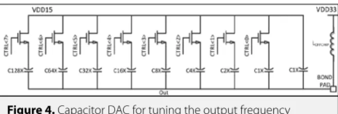
Figure 4 shows the capacitor array for each of the positive and negative output nodes. A binary weighted capacitor array is used to cover the frequency range of each of the four sub-bands. In order to maximize the capacitance density of the array, high density thin-oxide core MOS capacitors are used as long as the total parasitic capacitor permits. In order to comply with the re-liability requirements of these devices, 1.8V lower than the gate drive voltage needs to be applied to the bottom plate terminal. This corresponds to 1.5V since the output of the amplifier has 3.3V DC through the load inductor, hence a DC supply of this value was used to terminate the bottom plate side of the capac-itor. The use of 1.5V also enables the use of core devices as ar-ray switches, which is advantageous due to the reduces turn-on resistance and parasitic capacitance. Each time the array setting is incremented or decremented by one, the center frequency of the LC filter jumps up or down. The Least-Significant-Bit (LSB) of the array was chosen to give less than 1dB roll-off from the Figure 2. Output multiplexing network
Figure 3. Small signal schematic of a common gate amplifier with
off-chip inductor model
center gain to the intersections of the gain curves for two subse-quent tuning settings as shown in Figure 5.
Figure 6 shows the equivalent output impedance network for one of the output branches. The signal current from the cascode node is given by iC and flows into the output impedance to generate the output voltage. L is the external inductor used for tuning at the out-put node and CT is the equivalent total capacitance at the output. RL and RC denote the series resistances with the inductor and the ca-pacitor respectively. RL is composed of metal sheet resistance and RC is composed of resistances of the switches in the capacitance array in addition to metal sheet resistances. These resistances have a big im-pact on reducing the quality factor (Q) of the output load network, hence they need to be minimized. CN and RN are the equivalent load capacitance due to the next stage and the series resistance due to signal routing traces and intrinsic gate resistances respectively. In order to find the equivalent output network impedance, we can write KCL at the output node and derive ZOut=VOut/iC. This analysis gives the output admittance to be:
(3) This equation is the most general form for the equivalent out-put admittance and it is difficult to get any insight from it. CN is the gate capacitance for the next stage and is usually much smaller than CT in the network. RN is mostly the routing
resis-tance and can be comparable or smaller than RC since the latter is composed of routing and switch resistances. For the sake of simplicity, we can assume that the RN-CN network will be much smaller than the RC-CT branch, hence can be ignored. We then
can write the equation for the output impedance as:
(4) And the gain of the amplifier is given by:
(5) It is apparent from equation (4) that the network resonates at the frequency given in (2), where s2 term is equal to -1/LC
T.
When RL and RC values are close to each other and L is much
larger than CTRCRL term, output impedance simplifies to: (6) As expected, this equation suggests that for increasing RC and RL values, the equivalent load impedance goes down. Further-more, a minimum L/CT ratio has to be kept to ensure that the
amplifier has the minimum required gain. This is another rea-son to divide up the whole frequency range to 4 sub-bands since a large tuning range for the capacitor increases its value to a range that may be comparable to L value. Figure 6 shows how the impedance of the load network varies for varying RL and RC values using the actual design values for L and CT. It is apparent that as the RL and RC values increase a lot more than 1 Ω range, the output impedance scales down considerably. This has two consequences; the gain of the amplifier goes down and the rejection for blockers offset from the center frequen-cy is reduced. It is apparent from the figure that even with 1 Ω series resistance with the inductor and capacitor, the rejec-tion at 20% offset is around 10 dB, which is what we aim in this design. Consequently, layout techniques to reduce the series resistance with the external inductor and integrated capacitor array is very critical and are employed in this design.
Noise Figure
During operation, the amplifier is configured as a cascode am-plifier working in one of the sub-bands mentioned in Part 2.2 above. Consequently, input referred noise of the amplifier will be that of a differential cascode amplifier and is given by [9, 10]:
(7) where k is the Boltzman’s constant, γ is a technology depen-dent scaling factor for the process used, RL is the equivalent load resistance at the center frequency of the output tank and Figure 6. Schematic for the equivalent output load network.
Figure 5. Gain vs. Frequency for different tuning settings of the
RS is the source resistances. Using (7), noise figure of the ampli-fier can be calculated to be:
(8) A perfect differential matching at the input of the amplifier re-quires that 1/gm = RS/2. Using (11), we can show that the equa-tion simplifies to [10]:
(9) Equation (9) shows that the only way to control the NF of the amplifier is by increasing the gain by using a higher Q induc-tor. Otherwise, the NF is limited by the technology coefficients. Since the most important goal of this amplifier is to achieve higher filtering at the output by utilizing high-Q off-chip induc-tors, the design automatically minimizes the NF.
Distortion Analysis
In wide band receivers, linearity of the design blocks are ex-tremely important due to the fact that the there is a wide range
of incident frequencies that overload the system. As explained in the introduction, the specific system this amplifier is de-signed for may have a blocker of -10dBm at 20% offset when trying to receive a -120dBm desired signal and our design needs to be able to handle this power in full gain mode. In order to understand the distortion performance of the am-plifier designed, we can coarsely analyze it for linearity. Since the design is pseudo-differential, we can take half of the circuit and solve for distortion and the result will be the same for the differential amplifier for the fundamental tone and the odd harmonics. Even harmonics at the two outputs will be in phase and will cancel each other. One of the sub-bands of the am-plifier will be on at a given time, so the equivalent circuit for distortion analysis reduces to the one on the right in Figure 7. At the frequencies of interest, the cascode device acts as a ideal current buffer, therefore doesn’t introduce considerable dis-tortion. Furthermore, for the sake of simplicity, we will assume that the programmable capacitor array at the output is biased at deep inversion, hence small-signal at the output doesn’t cause considerable capacitance variation, which causes distor-tion. With these assumptions, the distortion of the single-end-ed amplifier is equal to that of a common gate amplifier with a source resistance. With Taylor Series expansion, the differential drain current of the amplifier can be written as [11]:
(10) (11) (12) (13) where μ is the mobility of electrons, Cox is the gate capacitance
den-sity and W/L is the gate-to-length ratio of the input transistors. It is apparent from Eq. (15) that for a fully matched amplifier, the second order distortion term is zero. Eq. (13) suggests that in order to min-imize the third order distortion, W/L ratio needs to be minmin-imized, Figure 7. Schematic of half-circuit for distortion calculations
while maximizing the gm of the input device. Transconductance (gm) of the input device is already decided on from Eq. (1) in order to have a adequate matching at the input port. Therefore, in order to mini-mize W/L ratio for a given gm value, VGS-VTH (also called VDSAT) of the
input device needs to be maximized. Additionally, careful design steps need to be taken to minimize the distortion due to secondary effects such as Channel Length Modulation. For this, the designer needs to make sure that the VDS is maximized for all the transistors.
The amplifier was designed in 0.18um standard CMOS process and layout was optimized to minimize parasitic resistors that limits the Q of the inductors. For this purpose, two pads for each output node was used to double-bond the outputs to the package pins and re-duce series resistor. This can be seen in the layout of the design in Figure 8. This figure shows the four subbands, the bonding pads for these, the input pads and the pads for supply and ground connec-tions. The design occupies an area of 2200μm-by-700μm without the bonding pads and 2500μm-by-850μm with the bonding pads.
Simulation Results
The design was verified across Process-Voltage-Temperature (PVT) using Cadence Spectre simulations. Post layout simulations were also performed to estimate the degradation in performance due to layout, bondwire and external inductor parasitics. The design works from 3.3V and 1.5V supplies for power supply and capacitor array ter-minations respectively, and consumes 20mA from the 3.3V supply. Figure 3 shows the inductor model used to model the exter-nal inductors [12] and Table 1 shows the values and the coeffi-cients for the inductors from Coilcraft.
Figure 9, 10 shows the gain and tuning curves for the amplifier. Fig-ure 8 shows the lowest tuned frequency and highest tuned frequen-cy for each of the sub-bands given in Table 1. Each band has overlap with the neighboring band at high and low ends of the range to make sure that there are no gaps in tuning in the whole frequency range of interest. The gain of the amplifier ranges from a minimum of 12dB to a maximum of 28dB across the whole band of 30-512MHz. This gain increase happens since the Q of the output tank increases as a function of frequency as we tune it higher within a sub-band. An attenuator following the amplifier can be used to limit the overall gain to a lower value in the case of high input power. Figure 9 shows how the amplifier tunes in the first sub-band of 30-50MHz by show-ing sample tunshow-ing settshow-ings that ranges from 0 to 255. Each sub-band has a total of 255 tuning steps as a result of 8 bit tuning control. Table 1. Design Parameters
BAND RS (Ω) RC (Ω) K L-ind (nH) Cind (fF) 30-50MHz 20 10m 165μ 81 56 50-100MHz 23 10m 72.2μ 35.7 59 100-200MHz 13 50m 48μ 21.9 54 200-512MHz 9 13m 32μ 12 58
Figure 9. Minimum and maximum tuning for each band Figure 1 1. Noise Figure vs. Frequency for the high-end tuning of the 30-50MHz sub-band
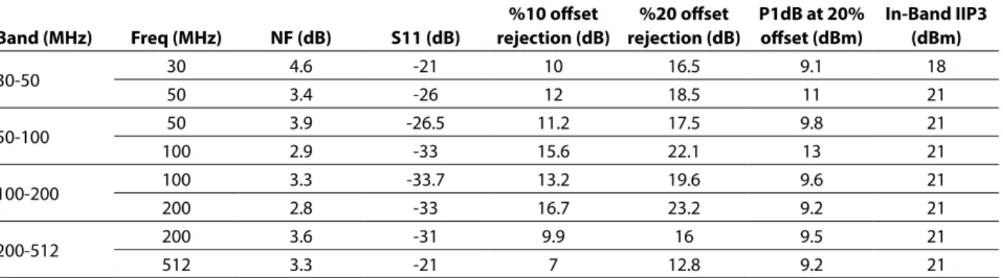
Figure 11 shows the Noise Figure of the amplifier when the out-put is tuned to the high end of the 30-50MHz sub-band. As the amplifier is tuned to different frequencies, the frequency where the minimum NF is achieved moves with the center frequency. Table 2 shows the NF at the low and high ends of each sub-band. Worst case NF is 4.6dB across the whole frequency range. Figure 12 shows the simulated impedance-match parameter (S11) result for the amplifier and it is less than -20dB across the whole frequency range of 30-512MHz. Table 2 gives S11 results at the low and high ends of each sub-band. The rejection of undesired signals at 10% and 20% frequency offset, which is one of the crit-ical specifications for the design, are also given in Table 2. These rejection amounts are adequate to reject the incoming undesired signal enough to keep it under control at the output of the am-plifier. The worst case 1dB compression point (P1dB) and the third order input intercept point (IIP3) for the amplifier are 9.1dBm and 18dBm, respectively, across the whole band as given in Table 2. Conclusion
In this paper, we have presented a wide-band tunable LNA that has been designed in 0.18μm CMOS process from UMC. The de-sign has been laid-out and post layout simulations were run to include the parasitic effects. The design dissipates 66mW from a 3.3V supply to meet the tough requirements of military radios. In the first part of the paper, the proposed design has been ana-lyzed for gain, tuning, matching, noise figure and distortion. The LNA works in the frequency range of 30-512MHz and achieves a minimum gain of 12dB across the whole range. Worst case Noise Figure was simulated to be 4.6dB and S11 is less than -20dB across
frequency and PVT. The design is highly linear and achieves a mini-mum of 9.1dBm P1dB and 18dBm IIP3 in worst case settings. References
1. B Taddiken, W Ezell, E Mumper, K Clayton, J Douglass, V Birleson, J Esquivel, O Werther, A Schneider, Bolton J, et al. Broadband tuner on a chip for cable modem, HDTV, and legacy analog standards. In: IEEE RFIC Symposium; 10 - 13 June 2000; Boston, MA, USA. Pis-cataway, NJ, USA. pp. 17-20. [CrossRef]
2. M Hajirostam and K Martin. On-chip broadband tuner design for cable mo-dem and digital CATV. In: IEEE 48th Midwest Symposium on Circuits and Systems; 7 - 10 August 2005; Cincinnati, OH, USA. pp. 1374 - 1377. [CrossRef]
3. D Im, I Nam, K Lee. A CMOS active feedback balun-LNA with high IIP2 for wideband digital TV receivers. IEEE T-MTT, 3566-3579, Dec. 2010. 4. J Kim and J Silva-Martinez. Wideband inductorless balun-LNA
employing feedback for low-power low-voltage applications. IEEE
T-MTT, 2833-2842, Sep. 2012.
5. EA Sobhy, AA Helmy, S Hoyos, K Entesari, E Sanchez-Sinencio. A 2.8mW Sub – 2dB Noise-Figure Inductorless Wideband CMOS LNA Employing Multiple Feedback. IEEE Trans. Microwave. Theory Tech., pp. 652-664, 2011.
6. F Bruccoleri, EAM Klumperink, B Nauta. Wide-band CMOS low-noise amplifier exploiting thermal low-noise cancellation. IEEE JSSC, pp. 275-282, Feb. 2004.
7. PR Gray, RG Meyer. Analysis and Design of Analog Integrated Cir-cuits. 3rd ed, New York, NY, USA: Wiley, 1993.
8. http://www.coilcraft.com/0603ls.cfm#table
9. TH Lee. Design of CMOS RF Integrated Circuits. Cambridge Univer-sity Press, 1998.
10. B Razavi. RF Microelectronic. New Jersey, NJ, USA: Prentice Hall, 1997. 11. Meyer RG. EE242 Course Reader, UC Berkeley, Berkeley, CA, USA,
Fall 1999.
12. http://www.coilcraft.com/0603CS.cfm
Table 2. Performance results
Band (MHz) Freq (MHz) NF (dB) S11 (dB) rejection (dB)%10 offset rejection (dB)%20 offset P1dB at 20% offset (dBm) In-Band IIP3 (dBm)
30-50 30 4.6 -21 10 16.5 9.1 18 50 3.4 -26 12 18.5 11 21 50-100 50 3.9 -26.5 11.2 17.5 9.8 21 100 2.9 -33 15.6 22.1 13 21 100-200 100 3.3 -33.7 13.2 19.6 9.6 21 200 2.8 -33 16.7 23.2 9.2 21 200-512 200 3.6 -31 9.9 16 9.5 21 512 3.3 -21 7 12.8 9.2 21
NF: noise figure; P1dB: 1-dB compression point; IIP3: 3rd order input intercept point
Hakan Doğan received his B.S. degree in electrical engineering from University of Southern California (USC), Los Angeles, in 1999, and the M.S. and Ph.D. degrees in electrical engineering from the University of California at Berkeley in 2001 and 2005, respectively. He is currently an Assistant Professor in the Electrical and Electronics Engineering Department at İstanbul Medipol University, İstanbul, Turkey. His research interests are in RF/Analog/Mixed Signal circuit design, end-to-end wire-less and wireline communication system design. Previously, he was an Assistant Professor in the Electrical and Electronics Engineering Department at Istanbul Sehir University, Istanbul, Turkey, from 2013 to 2017. He was with Qualcomm-Atheros and Atheros Communications San Jose, CA from 2005 to 2013, where he was involved with dual-band wireless-LAN trans-ceiver, Bluetooth transtrans-ceiver, PLC transceiver and GPS receiver chipset designs. In the summer of 2000, he worked in HP Labs, where he was involved with the design of clock and data recovery circuits. During the two consecutive summers, he was with Maxim Integrated Circuits, involved with the design of cable modem tuners and satellite receivers.

![Figure 3 shows the inductor model used to model the exter- exter-nal inductors [12] and Table 1 shows the values and the coeffi-cients for the inductors from Coilcraft.](https://thumb-eu.123doks.com/thumbv2/9libnet/5450850.104880/6.829.72.642.460.1068/figure-inductor-inductors-table-values-coeffi-inductors-coilcraft.webp)