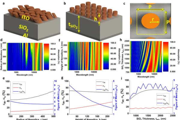
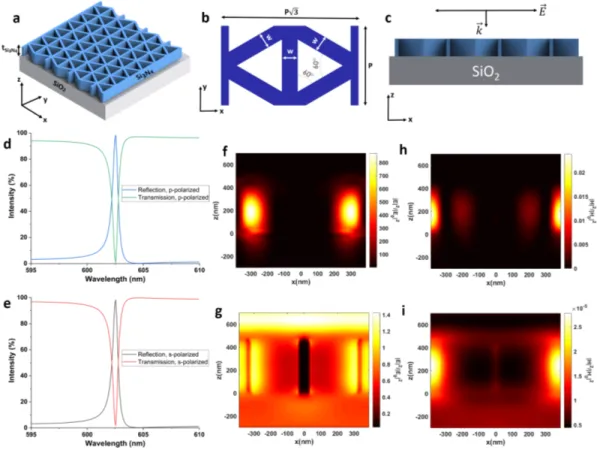
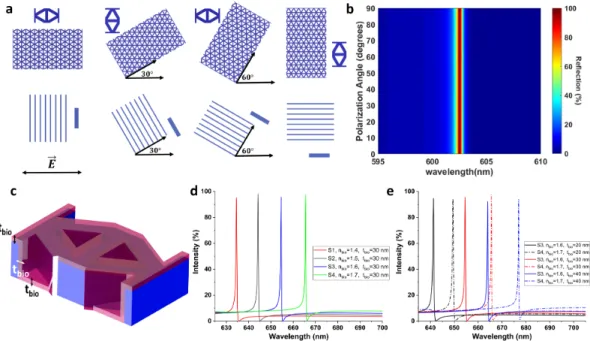
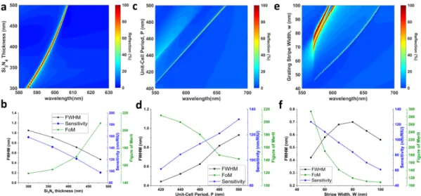
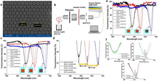
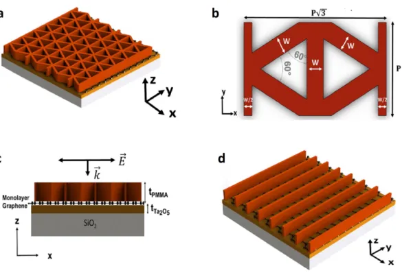
Dielectric metasurfaces as passive radiative coolers, colorimetric refractive index sensors, color filters, and one-way perfect absorber/reflectors with transparent sidebands
Tam metin
Şekil
Benzer Belgeler
The noise level of the seed signal, which can be further degraded in the amplifier, and the noise added in the amplifier, which is transferred from the pump source,
In this section we describe the improvements we have made on the DST attack which reduce the precomputation time, key search time, space, and plaintext complexities of the attack..
She would then ask questions that prompt children to think deeply about the new words as they play: “I can’t find the rake, do you think a shovel will work to pick the
Section 3 introduces a key jump operator and successive approximations to the value function of the auxiliary optimal stopping problem, whose solution is explicitly identified,
Bu çalışmada bir ninni söyleyicisi olması dolayısıyla sanatkâr olarak kabul edilebilecek annenin, o sırada ninninin sözlerini neden değiştirme ihtiyacını hissettiği
Fur- thermore, for a quadratic Gaussian signaling game problem, conditions for the existence of affine equilibrium policies as well as general informative equilibria are presented
analysis on the solution space reveals that negative deviations from the good machine combinations lead to more significant decrease in simulation time, when compared with
This study investigates the transfer of labour market orientations by American multinational enterprises to their Turkish subsidiaries by focusing on the influences of macro-
