DESIGNS OF COMPACT OPTICAL
DEVICES BASED ON PERIODIC
META-STRUCTURES
a thesis
submitted to the department of electrical and
electronics engineering
and the graduate school of engineering and science
of bilkent university
in partial fulfillment of the requirements
for the degree of
master of science
By
Ahmet Emin Akosman
July, 2013
I certify that I have read this thesis and that in my opinion it is fully adequate, in scope and in quality, as a thesis for the degree of Master of Science.
Prof. Dr. Ekmel ¨Ozbay(Advisor)
I certify that I have read this thesis and that in my opinion it is fully adequate, in scope and in quality, as a thesis for the degree of Master of Science.
Assoc. Prof. Dr. O˘guz G¨ulseren
I certify that I have read this thesis and that in my opinion it is fully adequate, in scope and in quality, as a thesis for the degree of Master of Science.
Asst. Prof. Dr. Ali Kemal Okyay
Approved for the Graduate School of Engineering and Science:
Prof. Dr. Levent Onural Director of the Graduate School
ABSTRACT
DESIGNS OF COMPACT OPTICAL DEVICES BASED
ON PERIODIC META-STRUCTURES
Ahmet Emin Akosman
M.S. in Electrical and Electronics Engineering Supervisor: Prof. Dr. Ekmel ¨Ozbay
July, 2013
Manipulation of the flow of light is demanded for several applications such as communication, data storage, sensor, photovoltaic cells, microscopy, lasers and light emitting diodes for the purpose of designing compact, high-throughput and high efficiency optical devices. Nevertheless, the control of the propagation of the light becomes much harder in devices with smaller geometries mostly because of diffractions, loss mechanisms and fabrication difficulties. Furthermore, materials that are already available in the nature do not provide unprecedented optical properties for nanoscale optical applications. Due to this fact that fabrication of artificial materials is needed for utilizing novel and intriguing optical devices. For this purpose, some relatively new research fields have emerged like photonic crys-tals, metamaterials and high contrast gratings. We propose several designs based on aforementioned meta-structures to achieve compact and practically realizable optical devices. We presented compact optical demultiplexer, diode-like device and electro-optic modulator designs that are based on photonic crystals. We also proposed two circular polarizer designs based on metamaterials and high contrast gratings. Further, we investigated unidirectional transmission and polarization manipulation properties in chiral metamaterials. For most of the proposed de-signs, we also experimentally verified the numerical and theoretical findings. In conclusion, we can claim that the utilization of artifically structured materials give opportunity to realize the control of light much more easily in nanoscale designs.
Keywords: Photonic Crystals, Metamaterials, High Contrast Gratings, Slow Light, Optical Demultiplexing, Asymmetric Transmission, Circular Polarization.
¨
OZET
PER˙IYOD˙IK META-YAPILAR TABANLI OPT˙IK
AYGIT TASARIMLARI
Ahmet Emin Akosman
Elektrik Elektronik M¨uhendisli˘gi, Y¨uksek Lisans Tez Y¨oneticisi: Prof. Dr. Ekmel ¨Ozbay
Temmuz, 2013
˙Ileti¸sim, veri depolama, sens¨or, fotovoltaik h¨ucreler, mikroskopi, laser ve led gibi uygulamalarda kullanılmak ¨uzere kompakt, ¨uretimi kolay ve y¨uksek ver-imli optik aygıtların tasarlanabilmesi i¸cin ı¸sı˘gın hareketinin manip¨ulasyonu ¨onem arz etmektedir. Ancak, ı¸sı˘gın daha k¨u¸c¨uk boyutlarda yapı elemanlarına sahip malzemelerde ilerlemesinin kontrol¨u sa¸cılımlar, kayıplar ve fabrikasyon hataları nedeniyle olduk¸ca zor bir hal almaktadır. Ayrıca, nano boyutlarda, do˘gada hazır bulunan malzemeler de bizlere beklenmedik ve ¨ust¨un optik ¨ozellikler sunmamak-tadır. Bu nedenle, ilgin¸c ve ¨ust¨un optik ¨ozelliklere ula¸sabilmek i¸cin yapay olarak ¨
uretilen malzemelere ihtiya¸c duyulmaktadır. Bu ama¸cla, fotonik kristaller, meta-malzemeler ve y¨uksek kontrastlı ızgaralar gibi daha yeni sayılabilecek ara¸stırma alanları do˘gmu¸stur. Biz de yukarıda bahsedilen yapay malzemeleri kullanarak kompakt ve rahat ¨uretilebilir optik aygıt tasarımları sunmaktayız. Fotonik kristaller kullarak optik ¸coklayıcı, diyot ve elektro-optik mod¨ulat¨or tasarımları olu¸sturduk. Metamalzemeler ve y¨uksek kontrastlı ızgaralar tabanlı dairesel polar-izasyon ¨uretimi yapan optik aygıt tasarımı ¸calı¸smalarında bulunduk. Son olarak ise, kiral metamalzemelerde tek y¨onl¨u iletim ve polarizasyon manip¨ulasyonu fenomenlerini inceledik. C¸ o˘gu ¸calı¸smamız i¸cin, elde etti˘gimiz teorik ve n¨umerik bulguları deneysel sonu¸clarla do˘grulamayı ba¸sardık. Sonu¸c olarak ise, yapay olarak ¨uretilmi¸s yapıların nano boyut tasarımlarda ı¸sı˘gın kontrol edilmesi i¸cin bizlere ¨onemli fırsatlar do˘gurabilece˘gi bilgisine ula¸stık.
Anahtar s¨ozc¨ukler : Fotonik Kristaller, Metamalzemeler, Y¨uksek Kontrastlı Iz-garalar, Yava¸s I¸sık, Optik C¸ oklama, Asimetrik ˙Iletim, Dairesel Polarizasyon.
Acknowledgements
I acknowledge that I am grateful to Prof. Dr. Ekmel Ozbay for his guidance, support and strong motivation throughout my graduate study.
I would like to thank to the Scientific and Technological Research Council of Turkey (TUBITAK) and TUBITAK BIDEB providing me Graduate Education Scholarship (BIDEB 2210) for two years.
I would like to thank to the members of my thesis committee, Assoc. Prof. Dr. O˘guz G¨ulseren and Asst. Prof. Dr. Ali Kemal Okyay, for reading the manuscript and commenting on the thesis.
As you all may know, graduate study is a mentally and physically challenging period. During this grueling period, I would like to express my gratitude to all my friends and colleagues who never withdraw their moral supports for me. Nonetheless, I would like to express that I feel very fortunate that I have met two valuable friends, Mehmet Mutlu and Sayim Gokyar. As a graduate student who has the similar ambitions and academic goals with me, Mehmet always helped me to keep my motivation high and tried to condole me in my saddest moments. As a friend from the department, Sayim also always listened my complaints and shared my feelings during these 3 years of Masters study. I have always felt that I have two more brothers about them.
I can never forget the morale support of my family during this period. Their love, guidance, motivation are invaluable to me. I have usually felt the regret that my complaints also made them upset. I am more than grateful to my dad, my mum and my brother, Furkan.
Last but not the least, I am indebted to my wife, Bedia, for her boundless and endless love. She has brought the brightest color onto my life with her morale support.
Contents
1 Introduction 2
2 Compact Optical Devices Based on Photonic Crystals 6
2.1 Introduction . . . 6
2.2 Slow Light in Photonic Crystals & Tight Binding Mechanism . . . 10
2.3 Optical De-multiplexer Design by Utilizing Slow Light in Photonic Crystals . . . 16
2.3.1 Optical De-multiplexing Methodology . . . 17
2.3.2 Single Wavelength Extraction . . . 18
2.3.3 Frequency Division Demultiplexing . . . 29
2.4 Optical Diode-like Devices based on Graded Photonic Crystals . . 38
2.4.1 Asymmetric Light Propagation Methodology . . . 39
2.4.2 Numerical Results of the Proposed Device & Experimental Verification . . . 41
2.5 Compact Photonic Crystal based Fabry-Perot Cavity Design for Electrooptic Modulation . . . 51
CONTENTS vii
2.5.1 Proposed Cavity and Sensitivity to Changes in Dielectic
Permittivity . . . 53
3 Circular Polarization Generation and Asymmetric Transmission Utilizing Chiral Metamaterials 64 3.1 Introduction . . . 64
3.2 Circular Polarizer based on Chiral Metamaterials . . . 67
3.3 Polarization Angle Dependent Rotation . . . 73
3.3.1 Proposed Geometry . . . 74
3.3.2 Numerical Results . . . 75
3.3.3 Experimental Results . . . 78
3.3.4 Formulation . . . 80
3.3.5 Surface Currents . . . 83
3.4 Diodelike Asymmetric Transmission . . . 84
3.4.1 General Idea . . . 85
3.4.2 Method . . . 87
3.4.3 Results and Discussion . . . 88
3.4.4 Eigenstate Interpretation . . . 92
4 Circular Polarizer Design based on High-Contrast Gratings 94 4.1 Introduction . . . 94 4.2 Theoretical and Numerical Investigations of the Proposed Structure 95
CONTENTS viii 4.3 Experimental Verification . . . 101 4.3.1 Proposed Geometry . . . 101 4.3.2 Numerical Results . . . 103 4.3.3 Fabrication . . . 106 4.3.4 Experimental Setup . . . 106 4.3.5 Experimental Results . . . 108 5 Conclusions 110 Bibliography 115 A Publication List 132
List of Figures
2.1 (a) The dispersion relation under transverse magnetic (TM) field excitation of the two dimensional PC waveguide structure; the black curve is the waveguide mode. (b) The super-cell of the PC coupled cavity configuration. The dashed lines enclose a coupled cavity waveguide, which has smaller coupled cavities (c) The dis-persion relation of the PC coupled cavity structure, the studied waveguide bands are given bold, which are observed to be approx-imately flat bands. (d) The complete PC coupled cavity configu-ration. . . 13 2.2 (a) Single PC cavity formation. (b) Double PC cavity formation
to observe eigen-mode splitting. (c) The transmission spectra for the single and double cavity structures. (d) The comparison of dis-persion relations of a selected waveguide band of the PC coupled cavity structure, which is constructed by the demonstrated cavi-ties. (e) The comparison of the numerical and theoretical group index values. . . 14 2.3 (a) The steady-state electric field distribution when the wavelength
of incident light corresponds to a propagating mode within the PC waveguide. (b) The field distribution for a different frequency, which is in the vicinity of the slow light regime. The same PCW is used in both cases. . . 19
LIST OF FIGURES x
2.4 The schematic of the device that is designed for the wavelength de-multiplexing. The different wavelengths are spatially separated at different locations along the x-direction. The complete structure is composed of three PCWs of different dielectric filling factors. . 20 2.5 The relation between the waveguide band cut-off frequency and the
dielectric filling factor. The highlighted frequencies correspond to the selected PCW sections. . . 21 2.6 (a) The evolution of the waveguide bands due to the different
di-electric filling factors, (b) the enlarged view of the vicinity of the slow light region, where the dashed lines correspond to the oper-ating frequencies. . . 22 2.7 The output frequency spectra of the channels of each PCW section
that has a r/a ratio of (a) 0.22, (b) 0.2, (c) 0.18, respectively. . . . 24 2.8 The steady-state electric field profiles of the three de-multiplexed
frequencies for each waveguide channel where the input beam is placed 5a away from the PC structure, (a) a/λ = 0.3086, (b) a/λ = 0.3158, (c) a/λ = 0.3247, (d) the steady-state electric field profile of an unselected frequency, which has a normalized frequency of a/λ = 0.34. . . 28 2.9 The spatial distributions of the operating frequencies at three
out-put channels in x-direction. The outout-put levels are calculated nearly 5a away from the output channels. The green dashed lines show the positions of the output channels in x-direction. . . 29 2.10 The geometry of the proposed DEMUX structure. The design
consists of two cascaded PCWs with unequal waveguide widths w1
and w2, respectively. The radii of the dielectric rods and the lattice
LIST OF FIGURES xi
2.11 (a) The dispersion diagram of a two-dimensional classical PC with a r/a ratio of 0.24 and a dielectric constant of 12. (b) The evolution of the waveguide band with respect to the waveguide width. The blue and red lines correspond to the widths for the DEMUX design. The PCW widths are altered linearly from 1.6a to 2.4a with an increment of 0.5a . . . 33 2.12 The transmission spectra of the output channels. The inset shows
the enlarged view of the de-multiplexed frequency intervals. . . 34 2.13 The spatial distributions of the pulses with normalized frequencies
of (a) a/λ = 0.2905 and (b) a/λ = 0.3105 that correspond to the centers of the de-multiplexed frequency bands at PC1 and PC2 sections, respectively. . . 36 2.14 The spatial distributions of the center frequencies of the
de-multiplexed frequency bands at the output channels along the x-direction. The vertical green dashed lines correspond to the posi-tions of the output channels. . . 37 2.15 Schematic representation of a chirped photonic crystal waveguide
that enables lights asymmetric propagation is provided. (a) and (b) correspond to left-to-right and right-to-left propagation, re-spectively. Yellow boxes in (a) show unit cell variations along the propagation direction. . . 41 2.16 The detailed presentations of the intensity distributions in
lin-early chirped waveguide configuration for the forward and back-ward light propagations are shown in (a) and (b), respectively. . . 42 2.17 (a) Schematic of a regular photonic crystal waveguide. (b) The
dispersion diagram of regular photonic crystal waveguide. (c) In-cident light propagation from left-to-right in the waveguide structure. 43
LIST OF FIGURES xii
2.18 (a) A photonic crystal waveguide that has linearly increased the distance separation between each neighboring column of rods. (b) The spectral content of the contrast ratio. The blue rectangle designates the selected frequency value. (c) Time-domain snapshot of propagation of light from left to right. (d) The transverse field profile across the end face of the structure. (e) The transverse field profile across the front side of the structure. (f) Time-domain snapshot of light propagation from right to left. . . 45 2.19 (a) Another chirped photonic crystal waveguide is shown. The
distance between each neighbouring column of rods increased in a parabolic pattern. (b) The spectral content of the contrast ratio. The blue rectangle designates the selected frequency value. (c) Time-domain snapshot of propagation of light from left to right. (d) The transverse field profile across the end face of the structure. (e) The transverse field profile across the front side of the structure. (f) Time-domain snapshot of propagation of light from right to left. 47 2.20 The simulated intensity distributions are provided at the outside
of the structure for microwave region. (a) The transverse field pro-file across the end face of the linearly chirped waveguide. (b) The transverse field profile across the front face of the same structure. (c) The transverse field profile across the end face of the paraboli-cally chirped waveguide. (d) The transverse field profile across the front face of the same structure. . . 48 2.21 The measured intensity distributions are provided at the outside
of the structure. (a) The transverse field profile across the end face of the linearly chirped waveguide. (b) The transverse field profile across the front face of the same structure. (c) The transverse field profile across the end face of the parabolically chirped waveguide. (d) The transverse field profile across the front face of the same structure. . . 50
LIST OF FIGURES xiii
2.22 The cross-sectional view of the proposed Fabry-Perot cavity geom-etry. The PC structure is assumed to be periodic and infinitely long along the ±y and ±x directions, respectively. The incident wave is assumed to be a plane wave propagating in the +z direc-tion. The transmission spectrum is obtained with the aid of the transmission monitor. . . 54 2.23 (a) The dispersion diagram and (b) power transmission spectrum
of the bulk PC structure. The red and the black curves represent the upper and the lower band of the PBG region, respectively. . 56 2.24 (a) Dispersion diagram and (b) power transmission spectrum of
the proposed Fabry-Perot type cavity. (c) The enlarged view of the cavity resonance that is enclosed by the dashed rectangle. . . 58 2.25 Power transmission spectra of the Fabry-Perot cavity for the cases
of (a) N=5, (b) N=6, and (c) N=7. The insets show the enlarged view of the regions enclosed by the dashed rectangles. . . 59 2.26 Electrical field distributions of the Fabry-Perot cavities for the
cases of (a) N=5, (b) N=6 and (c) N=7. The white dashed circles denote the positions of the holes. . . 60 2.27 Evolution of the spectral position of the cavity resonance with
respect to the change in the refractive index of the cavity region, ∆n. . . 61 2.28 Power transmission spectrum of the proposed Fabry-Perot type
cavity for the dual-polarization operation regime. . . 62 2.29 (a) Dispersion diagram and (b) power transmission spectrum of
the dual-mode operation regime of the proposed Fabry-Perot type cavity. . . 63
LIST OF FIGURES xiv
3.1 Geometry of the simulated and fabricated chiral metamaterial unit cell. . . 69 3.2 (a) Ratio of magnitudes of Tyx and Txx, and (b) phase difference
between Tyx and Txx. . . 70
3.3 (a) Numerical and (b) experimental results for the circular trans-formation coefficients. . . 71 3.4 Directions of the surface currents on the SRRs due to the incident
electric field polarized in the x-direction, at 5.1 GHz and 6.4 GHz 72 3.5 Geometry of the simulated and fabricated chiral metamaterial unit
cell. . . 75 3.6 Magnitudes of the linear transmission coefficients when the CMM
is illuminated by (a) x-polarized and (b) y-polarized incident waves. (c) The mutual phase differences between the transmis-sion coefficients. . . 76 3.7 (a) Ellipticities and (b) polarization azimuth rotation angles of the
transmitted waves for x-polarized and y-polarized illumination. . . 78 3.8 (a) Experimental magnitudes of Txx and Tyx, and (b) Txy and Tyy.
(c) Mutual phase differences obtained from the experiments. . . . 79 3.9 (a) Experimental ellipticies and (b) polarization rotations of the
transmitted waves due to x- and y-polarized incident waves. . . . 79 3.10 (a) Polarization angles of the transmitted linearly polarized waves
with respect to the polarization angle of the incident wave, at 6.2 GHz, for the −z and +z propagating waves. (b) Introduced polarization rotation to the −z and +z propagating waves with respect to the incident polarization angle, at 6.2 GHz. . . 82 3.11 Directions of the induced surface currents due to x-polarized plane
LIST OF FIGURES xv
3.12 Geometries of (a) layer A and (b) layer C. (c) Arrangement of A and C with respect to each other along with the mesh geometry and the stacking scheme. . . 87 3.13 |Txx| for (a) separate and (c) double layers, and |Tyx| for the same
(b) separate and (d) double layers. . . 89 3.14 Numerical and experimental transmission spectra for the ABS
stack, for x-polarized (a), (b) forward and (c), (d) backward propa-gating waves; (e), (f) numerical and experimental asymmetry factor. 90
4.1 Geometrical description of the HCG circular polarizer. The blue regions indicate the presence of Si, whereas the white regions are SiO2. . . 97
4.2 The normalized magnetic field distributions at λ0 = 1.55 µm inside
region II, (a) |Hy|/|H0| and (b) |Hx|/|H0| for TM and TE waves,
respectively. The distributions are obtained under the two-mode approximation. Grooves and ridges are separated by the white dashed lines and denoted by G and R, respectively. . . 98 4.3 (a) Field transmission coefficients for TM and TE waves and (b)
the phase difference between the transmission coefficients. . . 99 4.4 (a) Circular conversion coefficients obtained using the RCWA
and (b) the conversion efficiencies obtained from the RCWA and FDTD. The wavelength range for the FDTD result satisfying the 0.9 efficiency threshold is denoted by ∆λ. . . 100
4.5 Illustration of the proposed quarter-wave plate geometry. The dashed square box on the left denotes one period. The geometrical parameters are given by r = 220 nm, g = 350 nm, hg = 320 nm,
and Λ = 570 nm. In the theoretical and numerical consideration, for the sake of simplicity, regions I and III are assumed to be in-finite in the −z and +z directions, respectively. The materials constituting region III and the ridges in region II are sapphire and silicon, respectively, whereas region I is free-space. n0, nsi, and ns
represent the refractive indices of free-space, silicon, and sapphire, respectively. Grating direction is defined such that it corresponds to the y direction. . . 102 4.6 Numerical (a) TM and TE transmitted intensities, (b) circular
conversion coefficients, and (c) conversion efficiency spectrum ob-tained via FDTD simulations. The wavelength interval of opera-tion is denoted by ∆λ. The numerical conversion efficiency spec-trum yields a percent bandwidth of 42%. . . 104 4.7 (a) Zoomed out and (b) zoomed in top view SEM micrographs of
the fabricated HCG structure. In (b), the legends V1, V2, and V3 denote the geometrical parameters g, r, and Λ, respectively. . . . 105 4.8 Visual illustrations of the experimental setups that are utilized
for the measurement of (a) linear transmission coefficients and (b) circular conversion coefficients. The arrows, which lie inside the HCG samples and point upwards, denote the grating direction that is defined in the caption of Fig. 4.5. . . 107 4.9 Experimentally obtained (a) TM and TE transmitted intensities,
(b) circular conversion coefficients, and (c) conversion efficiency spectrum. The wavelength interval of operation is denoted by ∆λ. The experimental conversion efficiency spectrum yields a percent bandwidth of 33%. . . 108
Chapter 1
Introduction
Photonics is the research area that can beat the technical performances of the conventional electronic devices due to the ability of high speed data transmis-sion. Nevertheless, the manipulation of the properties and flow of light is less elucidated than the electrons for nanoscale device applications. Besides being a rather new research field, the conventional and already available materials in the nature also does not exhibit intriguing optical properties for the purpose of realizing optical devices and circuit elements. Some applications that the optical devices are needed for such as communication, data storage, sensor, photovoltaic cells, microscopy, lasers and light emitting diodes also require compact, high-throughput and high-efficiency designs. To meet the needs of this area, several rather new research areas have emerged like photonic crystals, metamaterials and high contrast gratings. The basic advantage of these periodic meta-structures is the opportunity of providing control of light at high frequencies in smaller scale. Photonic crystals are one, two or three dimensionally and periodically dis-tributed composite structures that are generally formed of dielectric or metallic constituents. The photonic band gap effect that inhibits the propagation of light at a certain frequency interval makes photonic crystals more intriguing [1–3]. In other words, the photonic band gap effect can be viewed as the analogous of the electronic band gap in semiconductor crystal. Moreover, several optical de-vices can be realized by means of the PBG effect such as waveguides with high
confinement and resonators with high quality factors.
In Chapter 2, we investigated and proposed several optical devices based on photonic crystals. First of all, the theoretical approach to the exhibition of slow light in photonic crystal waveguides are performed and the tight-binding mecha-nism is applied to the coupled photonic crystal waveguides for the incoming wave that has low group velocities. After the characteristics of the photonic crystal waveguides and the slow light regime, a novel optical demultiplexing methodol-ogy and design by utilizing the slow light regime in cascaded photonic crystal waveguides are proposed. The extraction of the targeted frequencies due to the spatial widening of the slow light modes in the waveguide, is both numerically and experimentally shown. Thereafter, a frequency division demultiplexer which extracts an interval of targeted frequencies instead of single frequency demulti-plexing is investigated. The numerical results of the proposed device also verified with the experimental efforts. Furthermore, the technical performance of the demultiplexer designs are compared with the conventional ones.
The second proposed optical device based on photonic crystals is a diode-like device that works as an analogue of an electronic diode for photons. Instead of regular photonic crystals, a graded photonic crystal waveguide is utilized for the purpose of achieving a spatially dynamic photonic band gap region and waveguide band. The guiding mechanism is unidirectionally provided by this utilization of graded waveguide. The experimental observations of the asymmetric deflection of the incoming wave for backward and forward illuminations are compared with the numerical results.
The last photonic crystal based proposal is a highly wavelength selective cavity design for electro-optic modulators. The photonic crystal cavity is formed by two bulk photonic crystal sections with a cavity region which is perpendicularly placed to the direction of the propagation. In other words, a classical Fabry-Perot type cavity is constructed by two side mirrors which are photonic crystal sections. Because of the utilization of Lithium Niobate for the substrate and the highly confined resonance modes in the substrate at the cavity region, we claimed that the effective dielectric permittivity of the substrate around the cavity can be
increased more than a bulk substrate under DC bias. The theoretical approach of the effective change in the permittivity is also investigated.
The third chapter is based on devices that are formed by chiral metamate-rials. Metamaterials are periodically distributed metallic elements that are in sub-wavelength scale which also makes them diffraction-free. Moreover, with the optimization of the geometrical parameters of the metallic constituents, negative refraction can be realized. Besides the classical metamaterials, Pendry claimed that negative refraction can be possible by using a chiral route in metamaterial based applications [4]. The most significant electromagnetic property of chiral metamaterials can be explained as the existence of the cross coupling between the electric and magnetic fields of the wave. This cross coupling also leads to different transmission coefficients under right hand circularly polarized and left hand circularly polarized wave illumination [5].
Firstly, we study the potential of an electrically thin, asymmetric chiral circu-lar pocircu-larizer structure, which is composed of isotropic materials, in obtaining LCP and RCP waves using a linearly polarized incident wave. The second proposed de-sign is a chiral metamaterial based polarization rotator which also has the similar operation mechanism with the circular polarizer which can also be explained with the difference in the transmission coefficients and the cross coupling between the electrical and magnetic fields. Similarly, our last study on chiral metamaterials is a unidirectional transmission device which is the optimized mechanism of the aformentioned asymmetric transmission effect. The optimization of the contrast ratio between the forward and backward waves is provided with the utilization of an additional sub wavelength metallic mesh between the metamaterial layers which are forming the chiral metamaterial structure. All of these studies and ef-fects based on chiral metamaterials are also experimentally observed and verified with the numerical results.
Chapter 4 is dedicated to the studies based on high contrast gratings. High contrast gratings are periodic structures with subwavelength periodicities. Due to exhibiting broadband and diffraction-free high reflectivity regimes, high-contrast gratings have attracted numerous researchers [6,7]. One should also note that
high refractive index difference between the consecutive constituents are required for the realization of broadband reflectivity regimes. Lastly, we propose a novel broadband circular polarizer design based on binary high contrast gratings. The numerical and theoretical analysis of the proposed device is investigated for a stand-alone structure. Additionally, a more realistic design on a substrate is proposed and the experimental verification of the proposed circular polarization generation operation is performed around the wavelength of λ = 1.55µm.
Chapter 2
Compact Optical Devices Based
on Photonic Crystals
2.1
Introduction
Photonic crystals (PCs) are one, two or three dimensionally and periodically distributed artifical composite structures that are usually consist of dielectric or metallic materials [8,9]. The most intriguing property for the PCs can be seen as the photonic band gap (PBG) effect [10]. PBG effect can be explained as the inhibition of the propagation of light inside the PC structures at a specific frequency interval [1]. This inhibition can be provided for any direction in the PC structures that is called as full PBG region. This PBG idea has spawned the field of PCs, which allows the manipulation of the flow of light in unexpected and new ways.
PBG effect in PC structures can be seen as the analogous of the electron band gap effect in semiconductors. The change in the properties of the photons in PC structures is in much the same way that ordinary semiconductor crystals effect the electrons [2,3]. Basically, the manipulation of the light has been performed by the general mechanism of total internal reflection. Total internal reflection occurs at the interface of two media with different refractive indices where the input wave is illuminated at the medium that has higher refractive index. However, this
mechanism can only be fully controllable when the surfaces are perfectly smooth. Thus, the practical realization of optical components is strictly limited for the utilization of total internal reflection mechanism. Nonetheless, PC structures offer a different way to manipulate the flow of the light that is based on the PBG effect.
For semiconductors, the periodic atomic lattice provides a periodic potential to the electrons that are propagating through the crystal. By means of the Bragg-like diffractions from the atoms in the crystal, a gap can open up to inhibit the propagation of the electrons in allowed energies. However, this inhibition is strongly dependent to the geometrical parameters of the periodic lattices and the strength of the periodic potential [3]. Likewise, this artificial potential is provided by the periodic distribution of dielectric media in macroscopic scales. If the ratio between the refractive indices of periodic constituents is high enough, then the Bragg scatterings at the interfaces provides the similar inhibition effect for the photons. One should note that the ideal PBG effect can only be observed in a perfect PC crystal. If a defect or mistake in the periodicity leads to localized states in these areas which makes the structure behaves as microcavity [11].
As it can be seen in the above paragraph, this manipulation of the crystal can also lead to new application areas. Considering the fact that introducing defects to the perfect PC crystal leads to the occuring of localized states, the pattern of the inclusions or extractions can be utilized in new optical phenomena. As it pre-viously mentioned, creating any type of defect inside the bulk PC structure can be utilized with the necessary geometrical optimizations for microcavity and res-onator applications [12]. In addition, extraction of a full line of constituents from the bulk PC structure which also looks like a classical waveguide with sidelines formed with PC sections, can be utilized as an optical guiding mechanism with high confinement [12,13]. Likewise, if this line defect is constructed as planar, this new structure can be utilized as a perfect mirror [14]. One should also note that all this effects can only occur if the periodicity of the structure is comparable to the wavelength of the light, which is also similar with the semiconductor crystals. Naturally, the theoretical description of the waves inside the PC structure
involves the solution of Maxwell’s equations in a periodic dielectric medium. If the constituents of the PC structure are purely dielectric, then Maxwell equations also indicate the solutions are scalable for the length and the frequency scale. In other words, a PC structure designed with pure dielectric materials exhibits the same fractional band gap for any length scale. Therefore, it is advantageous for the purpose of realizing the similar observations at microwave frequencies with milimeter scale feature sizes instead of using nanometer scale designs. Further, the properties of the PC structure with nanometer scale designs can easily be deduced by constructing the similar PC structure with scaling up all of the geometrical parameters and utilizing in lower frequencies.
If there is not any existence of external sources and currents, the simple form of the Maxwell equations can be written as [15]
{∇ × 1
ǫ(r)×}H(r) = ω2
c2H(r), (2.1)
where H(r) represents the magnetic field, ω is the frequency of the photon and ǫ(r) is the dielectric function of the media. If the dielectric function is perfectly periodic, then the possible solutions can be characterized by a wavevector k, and band index n. The k-space region of all allowed wavevectors is named as Brillouin zone and the collection of all solutions is formed as a band structure. If a region of frequencies with no solutions for any wavevector inside the Brillouin zone indicates that the PBG effect is observed at that frequency interval.
As the presence of mirror symmetry plane perpendicular to the constituents for two dimensional photonic crystals, it is possible to define the characteristics of the photons for both different polarizations with respect to the plane normal. These polarizations are called as transverse electric (TE) and transverse magnetic (TM) where the electric fields and the magnetic fields are perpendicular to the rods, respectively [15].
As it can deduced from the geometry of the two dimensional PC structure, the behaviours of the photons with different polarizations changes inside the struc-ture. For a general rule of thumb, TE band gaps are favoured in the connected
lattices and TM band gaps are favoured in a lattice of isolated high dielectric permittivity regions.
More information on the basics of PC structures can be found in several references [1–3,10,15]. In additional, more theoretical information is given in the subsections of this chapter below. The basic operation mechanisms of PC waveguides and cavities are investigated and explained in sections 2.2, 2.3.1 and
2.2
Slow Light in Photonic Crystals & Tight
Binding Mechanism
Slow light based applications have attracted numerous researcher because of the difficulties in the control of the optical signals in time domain [16]. The velocity of the light in vacuum is approximately c = 3 × 10⁻⁸m/s which corresponds to a
movement of 30 centimeters in 1ns. This ultrahigh speed is desred for effcent and fast data transmission in optical circuit. However, some additional mechanisms are required to slow the speed of light to handle the technical difficulties [16–18]. Next generation optical network devices require solutions that perform the task with low power consumption, high data rate and high throughput. In addition, all optical processing is needed to prevent the losses caused by the conversion of the signal from optical to electronic or vice versa. Optical switches and optical buffers can handle the problems of the transmission of the data optically by storing and arranging the timing of the optical data. In the current technology, the temporary storing and the delaying of the information flow is performed by mechanical delay lines. However, if the velocity of the light can be controlled, the response of the systems can be further accelerated. Moreover, decreasing the velocity of light can also provides the advantage of easier control of the optical phase in interferometric devices. Further, light-matter interactions can be enhanced by increasing the storing of the optical data for the purpose of improving the nonlinear effects, absorption and gain performances of the optical systems [19,20].
A significant amount of effort has been shown for the purpose of employing photonic crystal (PC) based structures in slow light applications [21–23]. As mentioned previously, PC structures offer intriguing dispersion properties such as photonic band gap (PBG) region. Moreover, cavities, waveguides and optical resonaters with high confinement properties can be designed by using PBG effect in PC structures. For PC waveguide structure, it has been shown that the velocity of the guided light is also lower than the speed of the light in regular media for some specified frequencies. The waveguide band lies inside the PBG region which also means that the field distributions of the guided modes experience strong confinement along transverse direction to the propoagation of the wave.
In addition, the zero group velocity near the edges of the waveguide band can be deduced by investigating the dispersion diagrams. However, the modes at the band edges are strongly dispersion because the relation between the frequency and the wave vectors are nonlinear which causes huge distortion in the propagation of the guided waves. Therefore, numerous studies are performed to decrease the group velocity dispersion (GVD) [24,25].
The most useful and meaningful definition of the velocity of light for slow light applications is the group velocity υg, which corresponds to the speed of the
pulse packet during the propagation. The group velocity is given by the inverse of the first-order dispersion [17]
υg = (
∂k ∂ω)
−1
(2.2) where ω and k are the angular frequency and the wavenumber, respectively. The effective refractive index that the slow light wave experiences is usually expressed with the group index
ng =
c υg
= c(∂k
∂ω) (2.3)
can also regarded as the slow-down factor of the speed of the light from the velocity in vacuum. In addition, the GVD can be calculated with the dispersion diagram and the group velocity diagram given as ∂2k/∂ω2.
A detailed investigation of this slow light formation has been made in a pre-vious study [26]. In this study, we focus on the theoretical aspect of the ultra slow modes in a PC waveguide constructed by using weakly coupled cavities. The behaviour of the ultra slow modes is explained by tight-binding (TB) formalism, which is used to express the nature of the waveguide modes in PCs [27]. TB description in PCs is an analog of classical wave TB explanation, which corre-sponds to the eigen-mode splitting of the evanescent cavity modes. The impurity states of the semiconductors are an equivalent mechanism to the defect modes of the PC cavity structures. The plane wave expansion (PWM) and the finite different time domain (FDTD) methods are used to calculate the group index values and eigen-mode splitting in the cavity modes. These calculations will be
used in extracting TB parameters and in the comparison of TB formalism and numerical results.
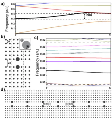
PC waveguides are constructed by introducing a line defect inside the PC structure to control the propagation of the incident EM field with high localiza-tion. The frequencies of the allowed modes are in the vicinity of the forbidden band of the PC, which is called photonic band gap. Furthermore, the modes are bounded by the waveguide mode that is created by the formation of linear defect. It can be deduced that the extra bound is a sign of high confinement and eventually the appearance of slow light modes. The confinement can be increased by introducing dielectric rods of different radii inside the waveguide and coupling cavities. Thus, the bound of the allowed modes is squeezed by the coupled cavity formation, which results in ultra low group velocity. The formation of the PBG inside a classical two dimensional PC waveguide and the alternative coupled cav-ity structure that is used to investigate the TB formalism in this study is shown in2.1.
The coupled cavities work as an impurity chain in the PC structure. Every cavity that is placed inside the structure creates a new resonance. The resonances eventually converge to a continuous band, creating a waveguide from the cavity chain. Strong coupling between the cavities causes a combined effect, which is crucial to realize the analogy of the TB mechanism.
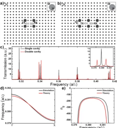
Each resonance occurring due to the waveguide can be represented by the eigenmodes of each cavity. The relation between the resonances can be deduced by introducing different number of coupled cavities into the system, which results with an eigenmode splitting scheme. The eigenmode splitting was expressed as a set of formulation [27]. The eigenmode splitting can be demonstrated by only two different configurations, which are the single cavity and double cavity structures. There is a single resonance peak for the single cavity case centered at ωc. For the
double cavity, the two resonance peaks split symmetrically obeying the following relation [27];
ω1,2 = ωc 1 ± β
1 ± α + ∆α (2.4)
Figure 2.1: (a) The dispersion relation under transverse magnetic (TM) field excitation of the two dimensional PC waveguide structure; the black curve is the waveguide mode. (b) The super-cell of the PC coupled cavity configuration. The dashed lines enclose a coupled cavity waveguide, which has smaller coupled cavities (c) The dispersion relation of the PC coupled cavity structure, the studied waveguide bands are given bold, which are observed to be approximately flat bands. (d) The complete PC coupled cavity configuration.
Figure 2.2: (a) Single PC cavity formation. (b) Double PC cavity formation to observe eigen-mode splitting. (c) The transmission spectra for the single and double cavity structures. (d) The comparison of dispersion relations of a selected waveguide band of the PC coupled cavity structure, which is constructed by the demonstrated cavities. (e) The comparison of the numerical and theoretical group index values.
and β thus it can be ignored. The splitting mechanism is demonstrated using the transmission data of the two configurations as given in Figs. 2.2(a) and 2.2(b).
The splitting separation decreases by introducing more cavities. The reso-nance peaks will emerge to each other and form a waveguide band, eventually. The dispersion relation of the occurring waveguide is given as [27];
ω2(k) = ω2 c
1 + 2β cos(kb)
1 + 2α cos(kb) (2.5)
where b is the intercavity distance. The parameters, αand β are ignorable com-pared to unity in flat waveguide modes as in the ultra slow modes. Thus, the
dispersion relation can be simplified as [27];
ω(k) = ωc(1 + κ cos(kb)) (2.6)
where κ is equal to β −α. The group index of a waveguide band can be calculated by combining Eq. 2.2, Eq. 2.3 and Eq. 2.6;
ng = −
c ωcκb sin(kb)
(2.7) The comparison of the tight-binding aspect and the numerical results of a slow light mode are shown in Fig. 2.2.
Furthermore, the relation between the group index and frequency can be made independent of the constant, κ, which results in an efficient method to calculate the group index by the knowledge of the transmission spectrum. The relation between κ and frequency is given as;
| κ |= ∆ω2ω
c
(2.8) where ∆ω is the frequency bandwidth of the waveguide. Combining Eq. 2.7 and Eq. 2.8, the final expression for group index is given as;
ng = −
2c
∆ωb sin(kb) (2.9)
It is apparent in Eq. 2.9 that group index is inversely related to bandwidth and inter-cavity distance. To sum up, tight-binding mechanism is applied to examine the characteristics of the slow light modes of a coupled cavity structure. This formulation provides flexibility in determining the group velocity of an incident field inside the PC by the knowledge of the transmission spectrum, if the waveg-uide band supports TB mechanism. Furthermore, the characteristics of ultra slow light modes can easily be determined without phase measurements.
2.3
Optical De-multiplexer Design by Utilizing
Slow Light in Photonic Crystals
As mentioned in the previous sections, PCs are strongly sensitive to the wave-length of the input source. This sensitivity also provides significant changes in the output transmission even for the slight geometrical modifications in the PC structures. The wavelength selectivity may be utilized for constructing op-tical devices that are commonly used in opop-tical communication systems such as optical filters which have the most usage in wavelength division multiplex-ing (WDM) systems [28–30]. Several de-multiplexer (DEMUX) methodologies, i.e. arrayed waveguide gratings (AWG), Bragg grating and thin film filters, have been proposed for achieving WDM operations that can be feasible for planar light wave circuits [31–33]. Some technical properties are desired such as compactness, cost-effectiveness, polarization independence and insensitivity, designs with low cross-talk and employing high spectral resolution for DEMUXs to achieve high quality optical communication [34,35]. The conventional designs that are men-tioned above mostly meet the demands regarding the resolution and cross-talk properties whereas the compact and cost effective designs have not reached state-of-art and feasible solutions [33]. PCs can be good candidates for new generation DEMUXs that are used in planar light wave circuits due to intriguing dispersion characteristics provided in smaller geometries.
Wavelength selectivity properties of PCs have been investigated to realize compact DEMUX designs by various methodologies such as using directional couplers, frequency selective micro PC cavities, multimode waveguides and em-ploying self imaging and super prism properties. In the work using PC directional couplers, demultiplexing operation is achieved by creating different resonance fre-quencies with different perturbations that are also responsible for the coupling of the operation frequencies into the coupled parallel waveguides which are employed as output channels [32,33,36]. Similar mechanism for creation of different reso-nance frequencies is also achieved by designing PC cavities with slightly different geometrical properties in Ref [36]. In the studies that multimode waveguides
are employed, the operation mechanism can be explained such that the waveg-uide modes in the photonic band gap (PBG) region also creates a mini stop band (MSB) where the modes experiences different group velocities [37–40]. The higher order waveguide modes have larger field penetration depth because of experienc-ing lower group velocities in which can be extracted from the output channels if the channel is thinned. The demultiplexing mechanism is finally achieved by con-structing different output channel thicknesses according to the group velocities of each waveguide mode. Moreover, demultiplexing mechanism is also investi-gated in the structures that consist of bulk PCs where the self-imaging and super prism properties are employed [41–43]. Further, a recent study proposes a gen-eral methodology for demultiplexing mechanism by employing coupling between different PC waveguides [44]. In all of these PC based DEMUX studies, it can be said that the large area and complex operation mechanisms can be eliminated by using PCs which provide strong wavelength selectivity due to rich dispersion characteristics that are occured for the wavelengths that are comparable to the period of the crystals.
2.3.1
Optical De-multiplexing Methodology
Optical de-multiplexing is mainly based on both creating different paths for dif-ferent operation wavelengths and prodive an effective extraction with minimum cross-talk between the output channels. The first step is designing a cascaded structure which has subsections that are sensitive to different wavelength inter-vals. In our studies, we constructed PC waveguides which has different geomet-rical periodicities which causes slight shifts in the allowed wavelengths to achieve different operation frequencies for each subsection. Secondly, we designed output channels such that each channel is only sensitive to the operation frequencies of the corresponding waveguide. This spatial sensitivity is achieved by matching the effective impedance of the output channel and the interested wavelength in the corresponding waveguide. In other words, the wavelengths that exhibit lower group velocities are extracted from the output channels. One should also note that the design of the output channels are arranged such that the slow light modes
with wider spatial distributions are easily penetrated into the output channels. By combining these two spatial and spectral selectivity properties, an efficient de-multiplexing operation is realized.
For the purpose of realizing spectral selectivity, we proposed two different mechanism which are using PC waveguide subsections with different periodicities and PC waveguides with different widths. In the first design, we aimed to achieve de-multiplexing of single wavelengths from each output channels. In the second design, we tried to achieve a DEMUX structure that the output channels collect an interval of wavelengths which is also called as frequency division DEMUX.
2.3.2
Single Wavelength Extraction
In single wavelength extraction operation, we report a DEMUX design using slow light phenomena in PC waveguides. We investigate the transmission characteris-tic of each output channel for each targeted single wavelength. The main target of this study is based on employing a DEMUX operation in a rather compact and small system. Thus, fulfilling aforementioned desired technical properties of DEMUX designs are not in the scope of this work.
The methodology of the wavelength selectivity mechanism is based on the modulation of the PBG region by altering the unit cell periodicity and electric-field distributions in the slow light regime. The dielectric filling factor of each PC section is altered that in turn modulates the bounds of the PBG region. The allowed waveguide modes lie inside the PBG region because there is not any other mechanism than PBG effect that supports guidance to propagating fields inside the waveguide. Therefore, other propagating modes leak out of the structure in the absence of guiding mechanism. As discussed in 2.2, the oscillation period along the longitudinal direction increases for the input wave if the wave experi-ences higher effective dielectric permittivity in the PC waveguide. Consequently, the increase in the longitudinal direction leads to penetration deeper toward the transverse plane to the propagation direction. Further, if the width of the PC is decreased on one side and coupled to a new PC waveguide channel which acts as
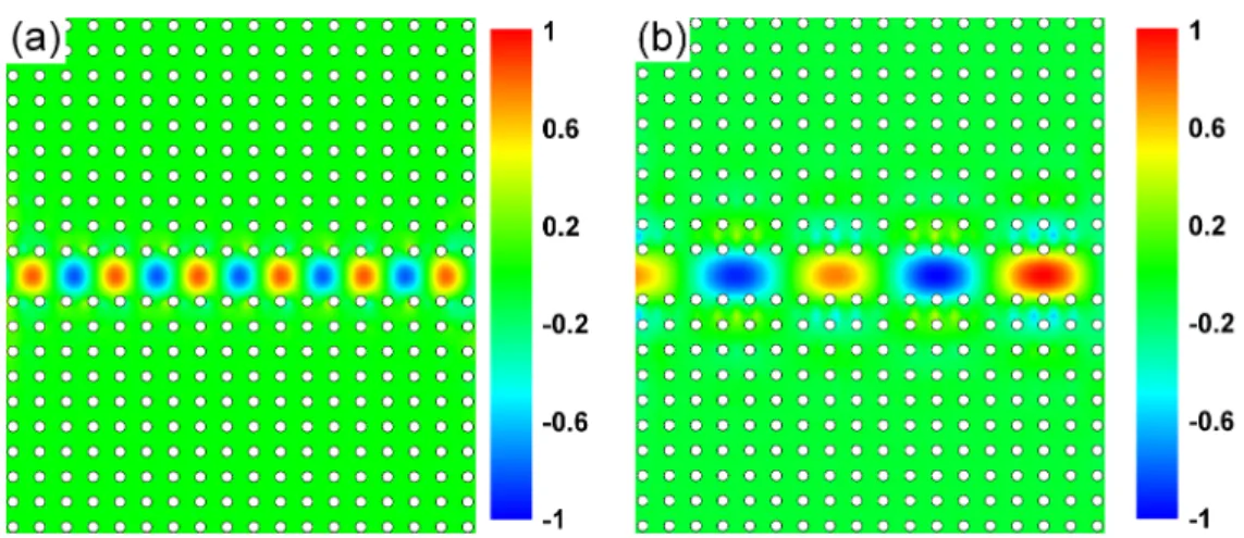
Figure 2.3: (a) The steady-state electric field distribution when the wavelength of incident light corresponds to a propagating mode within the PC waveguide. (b) The field distribution for a different frequency, which is in the vicinity of the slow light regime. The same PCW is used in both cases.
an output channel, the wavelengths that have broader spatial distribution in the transverse plane start to leak out at the thinned place of the PC waveguide into the output channel. If this mechanism is provided for PC sections with different periodicities, the extraction of different wavelengths, slow light regions, can be achieved. The difference in the spatial distributions of the guided regular and slow light modes can be seen in Fig. 2.3.
The geometry of the DEMUX design consists of three cascaded PC waveguide sections which have different unit cell periods, as shown in Fig. 2.4. The solid lines indicates the interfaces of each PC waveguide section. The main waveguide is constructed by the removal centerline row along the ΓX symmetry direction. The output channels are created by removing 2 rows of rods in the upper side of the main waveguide. The distance between two consecutive PC sections are kept as the periodicity of the section placed at the right part of the structure.
The numerical investigations of the PC structures are performed by utilizing finite-difference time-domain (FDTD) [45] which is a time-domain based numer-ical analysis technigue generally used for electrodynamic modeling. The simula-tion region is surrounded by perfectly matched layer (PML) to apply fully ab-sorbing boundary condition [46]. The unit-cell computational lattice a is divided into 32 grid points to sense the effect of incremental change in the periodicities
Figure 2.4: The schematic of the device that is designed for the wavelength de-multiplexing. The different wavelengths are spatially separated at different locations along the x-direction. The complete structure is composed of three PCWs of different dielectric filling factors.
for the purpose of investigating the wavelength shift in each output channel. The incoming wave is chosen as a Gaussian wave whose peak frequency is changed to excite the different output channels. The gaussian wave is intentionally selected to resemble the horn antennas which will be used in the experimental efforts. The input wave is set to TM polarization (i.e., the electric field component is perpendicular to the propagation plane) to create a PBG region and a highly confined waveguide mode for the proposed PC type.
The dielectric permittivity of the rods is selected as 9.61 in the numerical in-vestigations for the purpose of achieving a relatively high contrast between the air and the PC structures. The material is chosen as Alumina (Al2O3). In the case
of TM polarized light illumination, the spatial localizations of the electric field is mainly concentrated on the rods. Therefore, the high dielectric permittivity con-trast strengthens the interaction between the waves and the rods. Furthermore, if materials with higher dielectric permittivities are used, the separation between the operation wavelengths are expected to become larger.
As mentioned above, the DEMUX structure consists of three PC sections where the r/a ratios are slightly altered to achieve spectral selectivity. In other
Figure 2.5: The relation between the waveguide band cut-off frequency and the dielectric filling factor. The highlighted frequencies correspond to the selected PCW sections.
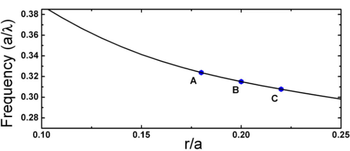
words, each PC section performs a testing by checking the wavelength of the input wave. The geometrical parameters of each PC section are selected by numerically investigating the cut-off frequencies of the waveguide bands of the consecutive PC waveguides. In Fig. 2.5, the selection of the r/a ratios of the consecutive PC waveguides is shown.
The first PC waveguide section has the largest rods, in other words highest dielectric filling factor (f ), where f equals to πr2/a2. The first PC waveguide
section has f = 15.2% and the radius of the rods is r1 = 0.22a (which is shown
as point C in Fig. 2.5). The filling factors of the second and the third section are decreased to 12.57% and 10.18%, respectively, by setting r2 = 0.20a and r3 =
0.18a (points B and A, respectively). As a result of decreasing the filling factors, the cut-off frequency of the PC waveguide increases as shown in Fig. 2.5.
The spectral properties and the evolution of the waveguide modes with the change in the r/a ratios of the PC structures can be seen in Fig. 2.6. The selec-tion of the operating wavelengths in Fig. 2.6(b) is based on the group velocities of those. As the group velocity of the wave is given with ∂w/∂k, the slow light regime of the waveguide modes in Fig. 2.6is in the vicinity of the band-edge. Al-though the minimum group velocity occurs at the band-edge (k =0) the targeted wavelengths are chosen as slightly lower because the highest output transmission
Figure 2.6: (a) The evolution of the waveguide bands due to the different dielectric filling factors, (b) the enlarged view of the vicinity of the slow light region, where the dashed lines correspond to the operating frequencies.
does not occur at the band-edge. There are two main reasons that the out-put transmission does not reach its maximum value along the waveguide band: Firstly, the waveguide modes near k =0 have higher impedances resulting in a higher impedance mismatch between the air and the main waveguide channel. Secondly, the maximum of the transmitted intensity does not occur at a mode that has a higher group velocity that is in the linear region of the waveguide mode as a result of the spatial distribution of the modes. Furthermore, the spa-tial distribution of the targeted mode is not only related with its frequency. The geometrical parameters of the PC waveguide is also effective on the spatial distri-bution. In other words, wider spatially distributed slow-light mode can achieved by increasing the length of the waveguide. Thus, the increase in the length of the PC waveguide results in a wider spatial distribution which is desired for the proposed DEMUX methodology. However, it can be deduced from the disper-sion diagrams that slower modes occur at the band-edge which also means that slower modes have the lowest frequency along the allowed waveguide modes in the PC waveguide. Consequently, the frequency shift of the peak transmission from the band-edge and the length of the PC waveguide are inversely proportional. The targeted operating frequencies are chosen by investigating the transmission properties of each PC waveguide section selected in Fig. 2.5 by considering the aforementioned explanations.
which shows both the numerical and experimental characteristics of output trans-missions. It can be seen that the transmission of the slow light modes are bounded from two sides which creates resonance like transmission characteristics. The lower frequency bound is caused by the PBG effect. The higher frequency bound is caused by the impedance mismatch and the spatial distributions of the modes. As it can be seen from the dispersion diagrams, the group velocity of the waveg-uide modes increases with the increase in the frequency. Therefore, the spatial distributions of the modes become less wide which means that the coupling be-tween the main waveguide channel and the output channel decreases. Conse-quently, each PC section behaves as a frequency filter and allows the propagation of only a portion of the modes that are already propagating in the main waveguide channel. This narrow band transmission can be seen as a coupling mechanism that has a quality factor of nearly 1000.
As mentioned previously, the design of the main waveguide and the output channels are optimized to maximize the output transmission at the operating wavelengths. The length of the PC waveguide and the geometrical parame-ters of the output channels are optimized to achieve the maximum output effi-ciency for this specific DEMUX device. The output channel is also designed as a wider waveguide than the waveguide to create a waveguide band which provides a lower effective dielectric permittivity for the targeted wavelength to achieve gradual permittivity transition from the main waveguide. Gradual transition in the permittivity also provides a more efficient match between the impedances of the main waveguide and the output channel which in turn results stronger cou-pling and higher output transmission. The design of the output channel can be achieved by constructing single- or multi-mode PC waveguide with a waveguide band which constitutes lower effective dielectric permittivity for the correspond-ing wavelengths. For an easier and more feasible design, the output channels are selected as multi-mode PC waveguides which has a width of 3a.
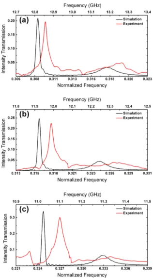
The selected wavelengths for the DEMUX operation are given in Fig. 2.7. As provided in Fig. 2.5, operating normalized frequencies for each PC waveguide sec-tion are selected as a1/λ1 = 0.3086, a2/λ2 = 0.3158, and a3/λ3 = 0.3247. For the
Figure 2.7: The output frequency spectra of the channels of each PCW section that has a r/a ratio of (a) 0.22, (b) 0.2, (c) 0.18, respectively.
the unit cell of each PC waveguide section is changed and the radii of rods are kept constant which can also be seen that each normalized frequency for each PC waveguide section is unique. Therefore, each targeted frequency is extracted from the corresponding output channel. In Fig. 2.7, the experimental output trans-mission spectra for each PC waveguide section are also shown for the purpose of comparison with the numerical results. The radii and the length of the alumina rods that are used in the experiments are selected as 0.158 cm and 15.32 cm, respectively. Consequently, the actual unit cell periods of each PC section can be calculated as 0.878 cm, 0.79 cm, 0.718 cm for r = 0.18a, r = 0.20a and r = 0.22a, respectively. The proposed PC waveguide sections is installed between two flat platforms that have comparable dielectric constants to that of free space. Two standard horn antennas are used to conduct the experiments. The antennas are both placed 10 cm away from the main and the output channels. For the purpose of measuring the transmission coefficients, HP-8510C network analyzer (Agilent Technologies, USA) is used. The demultiplexed frequencies and the similar out-put transmission spectra are observed in the experiments. However, because of the fabrication inconsistincies and impurities in the used materials, a slight fre-quency shift occured between the numerical and experimental results. Usage of alumina rods with finite length also cause power leakage in the z -direction which also can be seen in the experimental results. However, the leakage is minimized by means of using relative long rods (∼ 100r) compared to the operating wave-lengths. Moreover, the numerical and experimental results are in good agreement which can also be seen in Fig. 2.7. This good agreement also proves that the leakage in the z -direction is significantly prevented. In Fig. 2.7, the spectra of each section are shown separately because changing the unit cell period of the PC sections instead of radii of the rods to achieve the targeted normalized frequencies creates different normalized frequency axes for each PC waveguide section.
The demultiplexing mechanism occurs from the largest wavelength to the smallest one in the proposed PC structure. Each PC waveguide section behaves as a band pass filter and extracts the targeted wavelength into the output channel. Furthermore, assuming that the light has the appropriate wavelength to propa-gate through the first PCW, the second PCW checks the wavelength and allows
the light to pass if the wavelength of light corresponds to a propagating mode, in other words, whether it is distant from the slow light region. Otherwise, the wave will be extracted into the output channel due to its spatial distribution and the high coupling between the main waveguide and the output channel. Briefly, each PC section performs a similar task for different wavelength intervals. Each section either extracts the wave into the corresponding output channel or couples it to the next PC section. If the input wavelength is not extracted from one of the output channels, then the input will propagate through the main waveguide without any widening in the transverse direction and reaches the end of the main waveguide. One should also note that the injection ratio of the incoming wave between the main waveguide and the air is lower than that of a wave having a com-parable group velocity with air since modes in the slow light regime have higher impedances. Nonetheless, the injection ratio for the slow light modes can also be maximized by adding an additional input waveguide to achieve a more grad-ual transition in the effective permittivities which results in a better impedance match. Similar approach can be applied to the output channels to increase the overall extraction efficiency. Actually, this approach is already used for the pur-pose of designing output channels. The selection of a multi-mode waveguide with a width of 3a also provides a smoother impedance transition which in turn results a better coupling efficiency. This approach can also be thought as an incentive idea to design more efficient input and output couplers for PC based slow light devices. The output power at the output channels are smaller than the power at the output of the main waveguide when a single PC section is considered as the DEMUX device. However, the composite structure consisting multiple PC waveguide sections is also designed to inhibit the propagation of the wavelengths that are already demultiplexed in the previous PC sections. Then, the inhibited wavelengths reflect because they coincides with the PBG region of the next PC waveguide section. Therefore, the extracted power at output channels become larger than the power at the end of the main waveguide as a result of the reflec-tion of the previously de-multiplexed wavelengths at the surface of the next PC waveguide section.
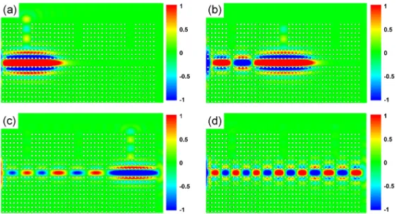
PC device are also simulated by keeping the unit cell period of each PC waveguide section and changing the radii of the rods to achieve the same filling factors. The steady-state electric field distributions of the targeted demultiplexed wavelengths are shown in Fig. 2.8. The electric field distribution for the normalized frequency a/λ = 0.3086 is shown in Fig. 2.8 (a). As it can be seen in the dispersion diagrams and in the transmission spectra, this input wavelength is coincides with the PBG region of the first PC waveguide section and below that of the second PC waveguide section. Therefore, the extraction of this wavelength is expected to be from the first output channel. The field distribution depicted in Fig. 2.8
(a) confirms that the extraction mechanism works properly. Likewise, the input frequency is set to a/λ = 0.3158 and the field distribution is shown in Fig.
2.8 (b). It is expected to observe that this wavelength propagates through the first PC waveguide section without any spatial widening and dropped to the output channel of the second PC waveguide section. Finally, for the wavelength at a/λ = 0.3247, the extraction from the third channel is shown in2.8 (c). Lastly, a wavelength that does not coincide with any of the slow light regimes of all PC waveguide section but also allowed to propagate through those, is selected and the propagation through the main waveguide can be seen in2.8 (d). As a result, it is observed using these figures that each PCW section filters a different wavelength and directs the selected wavelength toward the appropriate drop channel.
The spatial distributions of the demultiplexed wavelengths at the output chan-nels along the x -direction are also calculated and given in Fig. 2.9. The spectral content of the targeted wavelengths are determined by applying Fourier trans-form on the time domain data. The operating wavelengths are chosen such that, at these wavelengths, the output transmission is maximized whereas the cross-talk between the channels is minimized. As it can be observed in Fig. 2.9, the maximum level of the cross-talk for the first channel is calculated as -13.7 dB. The cross-talk levels for the second and the third channels are obtained as -15.6 dB and -28.7 dB, respectively. The proposed demultiplexing methodology also provides low cross-talk ratios at the output channels because of the inhibition of the wavelengths that are already demultiplexed in the previous output channels by utilizing the PBG regions of each PC waveguide section. The cross-talk ratios
Figure 2.8: The steady-state electric field profiles of the three de-multiplexed frequencies for each waveguide channel where the input beam is placed 5a away from the PC structure, (a) a/λ = 0.3086, (b) a/λ = 0.3158, (c) a/λ = 0.3247, (d) the steady-state electric field profile of an unselected frequency, which has a normalized frequency of a/λ = 0.34.
can further be decreased by a more effective selection of targeted wavelengths from the transmission spectra of the output channels. Moreover, cross-talk ratios can also be reduced by using rods that have higher dielectric permittivities which causes stronger separation of the selected wavelengths as a result of deeper inter-action between the PC structure and the waves that are in the slow light regime. In Fig. 2.9, it can be seen that the output distributions have sinc-like profile in x-direction which indicates that the coupling mechanism between the main waveguide and the output channels properly works. Moreover, sinc-like distri-bution profiles also show that the dispersion characteristics of the demultiplexed wavelengths in the main waveguide transform into the dispersion characteristics of the output channels.
The proposed methodology shows that the spectral and the spatial selectivity of the targeted wavelengths can be obtained. The performance of the proposed structure can be increased by geometrical modifications such as increasing the length of the PC waveguide sections which results in a peak transmission wave-length with a smaller group velocity. Furthermore, the spectral selectivity can be
Figure 2.9: The spatial distributions of the operating frequencies at three output channels in x-direction. The output levels are calculated nearly 5a away from the output channels. The green dashed lines show the positions of the output channels in x-direction.
increased by keeping the difference of the filling factors between the PC waveg-uide sections smaller. In other words, to demultiplex wavelengths with smaller shifts can be achieved by cascading PC waveguide sections with small changes in the filling factors. The number of the PC waveguide sections can be increased in order to demultiplex more than three wavelengths. Additional PC waveg-uide sections should also be carefully designed for the purpose of achieving low cross-talk ratio between the other channels by considering the overlap of the new targeted wavelength with the waveguide bands of the previous channels to in-hibit the transmission of the previously demultiplexed wavelengths. Lastly, .the usage of PC waveguide sections with equal lengths leads to a compact design, although the management of cross-talk between channels becomes more difficult as a consequence of the absence of the minimization of back reflections from each section.