https://doi.org/10.1007/s10854-020-03868-9
Intersection behavior of the current–voltage (I–V) characteristics
of the (Au/Ni)/HfAlO
3/n‑Si (MIS) structure depends on the lighting
intensity
Engin Arslan1,2 · Yosef Badali1 · Şemsettin Altındal4 · Ekmel Özbay2,3,5 Received: 20 April 2020 / Accepted: 24 June 2020 / Published online: 6 July 2020
© Springer Science+Business Media, LLC, part of Springer Nature 2020
Abstract
The current–voltage (I–V) and capacitance–voltage (C–V) behaviors of the (Au/Ni)/HfAlO3/n-Si (MIS) junctions at room temperature under white light with various intensities were investigated. The ln(I)–V curves show two linear behavior regions at about 1 V before and after the point of intersection that can be defined as two separate current-conduction (CMs) Mechanisms. The values of the ideality factor (n) and the zero-bias barrier height (ΦB0) were extracted using the slope
and intercept of the ln(I)–V curve before and after the intersection point based on lighting power. Although the ΦB0 values
decrease with increasing light power, n increases for two regions, and there is a strong linear relationship between them. The values of photo-current (Iph) increase with the increasing lighting power due to the formation of electron–hole pairs. The
slope of the double-logarithmic Iph–P was changed from 0.422 to 0.852, respectively, at − 2 V and − 9 V, which indicates the
ongoing distribution of Nss. In addition, the profile of surface states (Nss) ionized by light was obtained from the capacitance measured in dark and under lighting at 1 MHz. The Nss–V curve has two characteristic peaks that correspond to the region
of depletion and accumulation due to a special distribution of Nss and their restructuring and reordering under the effects of
lighting and an electric field.
1 Introduction
The metal–semiconductors (MS) and metal–insulator–semi-conductors (MIS) structures have long been a trendy tech-nology, such as integrated circuit diodes, MIS capacitors, photodiodes, and other applications. Especially the MIS photo-diode and photo-detector experiments have been get-ting deeper and broader in recent years [1–3]. The manu-facturing processes and the creation of an interface layer
between the metal and a semiconductor play significant roles in the performance of this structure, its barrier heights (BH), and conduction mechanisms (CMs) [4–6]. The reaction of the Schottky structure to the applied bias voltage, temper-ature, frequency, and intensity of light has a direct effect on certain optoelectronic devices. The performance of MS and MIS devices can be optimized by various factors, such as the choice of metal and semiconductor with acceptable work functions, appropriate doping (donor/acceptor atoms) level, interface layer, and its homogeneity and thickness, low density of Nss, low series resistance (Rs), and homogeneity of BH [7, 8]. Furthermore, the optical behavior and photo-response of a diode can be improved by changing the inter-face layer. The photo-current was stated to have low-voltage saturation characteristics due to the limitation of the minor-ity carrier. Because high-k materials play an important role in the efficiency of MIS structures, many researchers tried to prepare MIS devices with high-k thin films as the insulator layer to reduce saturation at low voltage [9, 10].
The HfO2 has drawn significant interest for both
resis-tive oxide and optical materials thanks to its strong ther-mal and chemical stability [11], high dielectric constant (~ 25) [12], and wide bandgap (5.8 eV) [13], and has a good * Engin Arslan
1 Department of Electrical and Electronics Engineering,
Antalya Bilim University, 07190 Antalya, Turkey
2 Nanotechnology Research Center, Bilkent University,
Bilkent, 06800 Ankara, Turkey
3 Department of Electrical and Electronics Engineering,
Bilkent University, Bilkent, 06800 Ankara, Turkey
4 Department of Physics, Faculty of Sciences, Gazi University,
Ankara, Turkey
5 Department of Physics, Bilkent University, Bilkent,
transmittance especially in ultraviolet light [14]. Depend-ing on the above-mentioned properties, the basic HfO2 has a vast range of applications involving resistive switching [15], UV anti-reflective film, and gate dielectrics in the Schottky structures [16–18]. However, there is a significant disadvantage for this substance, which is its poor thermal stability and the comparatively low crystallization tempera-ture (400–450 °C) [16]. These properties cause a significant increase in the leakage current if HfO2 films are incorporated
in a high-temperature MIS system. To increase the crystal-lization temperature and enhance the electrical properties of HfO2, it can be converted to alloy HfAlOx (hafnium
alu-minum) using aluminum oxide (Al2O3) intermixed [19–21].
Furthermore, the integration of the Al into HfO2 causes an increase in its dielectric constant and bandgap as well as decreases its hysteresis and charging defects. All of these properties of HfAlOx make it an excellent material for use in
MIS systems of future technology as an alternative to other dielectric materials.
The conduction mechanism of MS and MIS Schottky structures under the light can be quite different from those in the dark. These structures with oxide interface layers sometimes show a photo-response behavior [14, 18]. For this reason, current–voltage (I–V) measurements of such structures under different lighting intensities can give us important information about the basic current-conduction parameters such as CMs, BH, and performance of the struc-ture.[22, 23]. Generally, the capacitance values of an MIS structure and also the basic electrical parameters such as ideality factor (n), BH (ΦB0), series and shunt resistances
(Rs and Rsh), and the density of interface states (Nss) can be
strongly influenced by lighting intensity [24]. On the other hand, there are various theoretical and experimental studies investigating the point of intersection in the I–V graph of the MIS structure calculated at various temperatures. These studies have explained that the intersection point can occur due to the decrease in apparent barrier height with decreas-ing temperature and the presence of Rs [25–27].
There are several studies on the dielectric characteris-tics of the HfAlOx alloys, but none of the studies focus on
their photo-diode characteristics or their reaction to light as MIS structures, while the investigation of optical behavior plays a significant role in such studies and implementations of alloys. Therefore, it is important to investigate the light power-dependent electrical and optical characteristics. The present paper explores the key electrical parameters of (Au/ Ni)/HfAlO3/n-Si MIS structure such as n, BH, and Rs based
on the white light intensity. For this, both the forward and reverse bias I–V characteristics of this device were done at the light power range of 0–300 W. The experimental results show that the ln(I)–V curves display two linear sections that can be represented as two separate CMs before and after an intersection point. Furthermore, the voltage-dependent
capacitance behavior was measured in dark and under the illumination of 300 W light and the Nss was obtained from the measured capacitance values in dark and under illumination.
2 Experimental procedures
The phosphor-doped silicon wafer (n-Si) with ⟨100⟩ float zone, ~ 300 μm thickness, and 1 Ω cm resistivity was cleaned using RCA-1 and RCA-2 standard cleaning procedures to remove the metal ions, a thin oxide layer, and organic resi-dues of the wafer surface. The cleaned wafer was then moved to the thermal evaporation system and Al metal (99.999%) with a thickness of 300 nm was formed on the backside of n-Si at ~ 1 × 10⁻⁵ Pa. The formation of an Ohmic contact was
then annealed at 450 °C for 20 s in N2 ambient. The
produc-tion of devices continued with the growth of 80 nm ternary HfAlO3 alloys on the substrate using Cambridge Nanotech.
Inc. Savannah/S100 Atomic Layer Deposition (ALD) sys-tem. Deposition of 300 Cycles led to 80 nm of thin HfAlO3
film. H2O, Al(CH3)3, H2O, and Hf(NMe2)4 are used as pre-cursors and are successively added into the chamber to com-plete a cycle. In each cycle, the pulse and purge times are 0.015 s and 8 s, 0.015 s and 8 s, 0.015 s and 10 s, and 0.2 s and 15 s, respectively, for each precursor.
The atomic ratios of the hafnium (Hf), aluminum (Al), and oxygen (O) atoms in the HfAlO3 layer on n-Si substrate
were calculated using X-ray Photoelectron Spectroscopy (XPS) quantitative analysis. The thickness-dependent XPS profile of HfAlO3 layer confirmed that the average atomic
fractions are 19.2%, 21.9%, and 58.9% for Hf, Al, and O, respectively; therefore, the atomic ratios of the HfAlO film are very similar to 1:1:3. The thickness of the HfAlO3 lay-ers was confirmed using a cross-sectional scanning electron microscope (SEM) images as nominally 80 nm.
Using the thermal evaporation method at ~ 1 × 10⁻⁵ Pa,
the Ni(50 nm)/Au(200 nm) circular rectifier contacts with a 0.005 cm2 area were finally created on the HfAlO
3 surface.
Therefore, the fabrication of an (Au/Ni)/HfAlO3/n-Si MIS
structure was completed. The current–voltage (I–V) and capacitance–voltage (C–V) characteristics of the device are carried out using the source-meter Keithley-2400 and the impedance-meter HP 4192A LF, respectively, under the lightning of 0 and 300 W intensity range at room temperature.
3 Experimental results and discussions
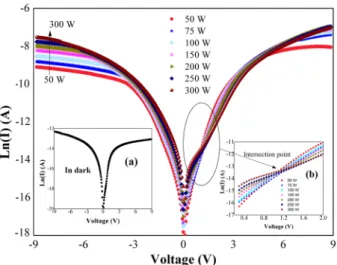
Figure 1 shows the measured ln(I)–V curves of the (Au/ Ni)/HfAlO3/n-Si structure in the broad light power range
0.05 V steps at room temperature. As depicted in the inset of Fig. 1, the ln(I)–V curves have an interesting feature in the forward bias region that has almost the common volt-age point at nearly 1 V. At this point, the current values are free from the influence of light power. Many experimental and theoretical studies have also reported similar behavior based on temperature or lighting [26–28]. According to Chand [25], the intersection can occur at the same point, but the ln(I)–V curves are bent for each basic barrier due to the current saturation effect of series resistance. For large structure diameter, this intersection point is shifted to a higher voltage region. Therefore, if we want to observe the intersection of I–V curves, we must reduce the structure diameter to a nanometer scale [27]. These observations in the intersection point of the forward bias ln(I)–V curves tend to be an unusual behavior compared to the ideal diode in the MS or MIS structure. With an increasing light power, the value of forwarding current decreases after the intersection point due to the lack of free carriers in both dark and low light power conditions. Therefore, although the value of Rs decreases before the intersection point with
increasing light intensity, it increases with increasing light intensity after the intersection. This behavior is very unex-pected in the nature of Schottky junctions and at first look, it is in contrast with the thermionic emission (TE) concept of the current-conduction mechanisms (CCMs).
According to the theory of thermionic emission (TE), the amount of current passing through the MS or MIS structure at a forward bias (V ≥ 3kT/q) is presented by [4–6]
In Eq. 1, the reverse bias saturation current (I0) is the expression terms in front of the brackets; the IRs is voltage
decrease over Rs; A* is the numerical value of Richardson
constant (= 112 A cm−2 K−2 for n-Si), and T is
the tempera-ture in Kelvin. Thus, for each lighting power, the value of
n and ΦB0 of the (Au/Ni)/HfAlO3/n-Si structure was
deter-mined from the slope and intercept of the ln(I)–V curves, respectively, as follows [4–6]:
The experimental values of n and ΦB0 were acquired from
Fig. 2a, b and they changed from 9.915 to 20.924 and 0.732 to 0.672 eV before the intersection point (between 0.30 and 0.7 V) and 15.882 to 23.637 and 0.692 to 0.676 eV after the intersection point (between 1.5 and 2.0 V), respectively. Table 1 summarizes the values of I0, n, ΦB0, and Rs derived
from Ohm’s law (Rs = V/I). As can be seen in Table 1 and Fig. 3, while the value of ΦB0 decreases with increasing
lighting power, n increases and there is a good linear relation between them before and after the intersection point that can be described by two different CMs.
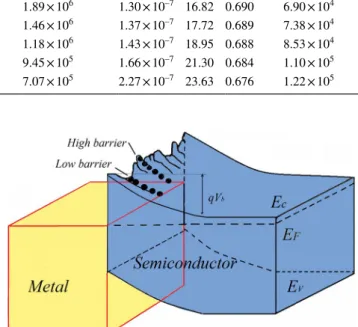
The higher values of n both in dark and under lighting refer to the presence of Nss, interface HfAlO3 layer, the
Gaussian distribution of BH (Fig. 4) at M/S interface, tun-neling current via dislocations in Schottky structures, and generation recombination [5, 6].
All of these findings demonstrate that the HfAlO3
inter-facial layer leads to enhanced light sensitivity as several electron–hole pairs can be produced near the junction under lighting. As seen in Figs. 1 and 5, the photo-current (Iph)
values increase with increased lighting particularly in the reverse bias region due to a strong electric field. Recombin-ing electron–hole pairs can obstruct the reverse bias region under a high electric field, but they can easily recombine in the forward bias region due to a low electric field value.
Typically, the photo-current or photo-response attitude of the solar cells or photodiodes can be described with the expression below [27, 29]:
here, Iph is the photo-current, A is a constant, P is the power
of lighting, and m is an exponent of lighting power. Figure 5
displays the ln(Iph)–ln(P) curves and the magnitude m was (1) I= AA∗T2 exp ( − q kTΦB0 )[ exp ( q(V− IRs ) nkT ) − 1 ] (2) n= q kT [ dV∕d(lnI)] (3) ΦB0= kT q ln ( AA∗T2 I0 ) (4) ln(Iph)= mln(P) + A
Fig. 1 The measured ln(I)–V curves of the (Au/Ni)/HfAlO3/n-Si
structure under lighting with various light intensities. The measured ln(I)–V curves in dark and the focused graph of the ln(I)–V curves between 0.3 and 2.0 V under lighting are shown in the insets (a) and (b), respectively
derived from their slope as 0.42 at − 2 V and 0.85 at − 9 V. These m values suggest the presence of Nss with energies
in forbidden bandgap between HfAlO3 interlayer and n-Si.
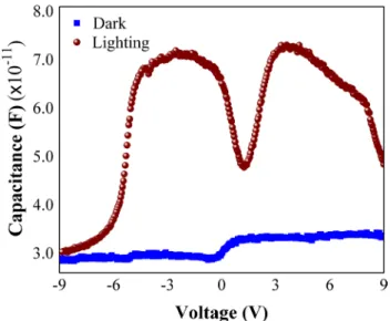
Figure 6 shows the voltage-dependent capacitance (C–V) curves of the (Au/Ni)/HfAlO3/n-Si structure in
dark and under 300 W lighting at a frequency of 1 MHz measured voltage values between − 9 and + 9 V. It is clear that the value of C is considerably increased under light and shows two peaks in the inversion (between − 5
Fig. 2 The focused ln(I)–V curves of the (Au/Ni)/HfAlO3/n-Si structure measured under lighting with various light power, a before and b after the intersection point
Table 1 Lighting based upon the electrical parameters of the (Au/Ni)/HfAlO3/n-Si structure
Before intersection point After intersection point
I0 (A) n ΦB0 (eV) Rs (Ω) (at 0.5 V) I0 (A) n ΦB0 (eV) Rs (Ω) (at 3 V)
0 W 4.29 × 10⁻⁹ 5.57 0.779 2.90 × 10⁷ – – – 3.85 × 10⁶ 50 W 2.66 × 10⁻⁸ 9.91 0.731 2.63 × 10⁶ 1.23 × 10⁻⁷ 15.88 0.692 6.60 × 10⁴ 100 W 5.36 × 10⁻⁸ 12.26 0.713 1.89 × 10⁶ 1.30 × 10⁻⁷ 16.82 0.690 6.90 × 10⁴ 150 W 8.47 × 10⁻⁸ 14.11 0.702 1.46 × 10⁶ 1.37 × 10⁻⁷ 17.72 0.689 7.38 × 10⁴ 200 W 1.26 × 10⁻⁷ 16.31 0.691 1.18 × 10⁶ 1.43 × 10⁻⁷ 18.95 0.688 8.53 × 10⁴ 250 W 1.85 × 10⁻⁷ 19.04 0.681 9.45 × 10⁵ 1.66 × 10⁻⁷ 21.30 0.684 1.10 × 10⁵ 300 W 2.71 × 10⁻⁷ 20.92 0.671 7.07 × 10⁵ 2.27 × 10⁻⁷ 23.63 0.676 1.22 × 10⁵
Fig. 3 The ΦB0–n curves of the (Au/Ni)/HfAlO3/n-Si structure before
and after the intersection point
and 1 V) and accumulation (between 1 and 9 V) regions. The observed two distinctive peaks with light effect in the C–V (Fig. 6) curve are the result of a special density distribution of Nss due to their restructuring and
reorder-ing. While the first peak is corresponding to the inversion region, the second peak is corresponding to the accumula-tion region. Therefore, the lighting-induced values of Nss
were acquired from the dark-lighting capacitance method (Cd − Cl) by using the following expression and are given in Fig. 7 [22].
As seen in Fig. 7, the voltage-dependent surface states’ profile (Nss–V) has two distinctive peaks like C–V curve.
This is evidence of the existence of localized surface states with two different regions and life times. These surface states are induced under an external force such as electric field, temperature, or light and they act as recombination centers that can be release or capture electronic charges. Therefore, in this work the lighting causes an increase in the capacitance value. The observed first peak in the C–V curve in the inversion region is only the result of surface states at HfAlO3/n-Si interface. However, the second peak in the accumulation region is the result of both series resist-ance and surface states. These results show that the surface states in the inversion region are more effective than that in the accumulation region. Similar two peaks’ behaviors in the C–V curve under radiation are also observed in the literature [30, 31].
4 Conclusion
In this study, both the forward and reverse bias I–V and C–V characteristics of the fabricated (Au/Ni)/HfAlO3/n-Si (MIS)
structures were investigated in the dark and under lighting in a wide voltage range (± 9 V) and at room temperature. The semi-logarithmic I–V curves for various lighting power have two linear parts before and after an intersection point at about 1 V. Such an interesting feature of these curves shows the existence of two different mechanisms of current (5) qANss= [(1∕Cd− 1∕Ci )−1 − (1∕Cl− 1∕Ci )−1] .
Fig. 5 The ln(Iph)–ln(P) curves of the (Au/Ni)/HfAlO3/n-Si structure
Fig. 6 The C–V curves of the (Au/Ni)/HfAlO3/n-Si structure in dark
and under the light at a power of 300 W at 1 MHz
Fig. 7 The voltage-dependent profile of Nss for (Au/Ni)/HfAlO3/n-Si
transport. The obtained experimental values of n and ΦB0
using the slope and intercept of ln(I)–V curves are found to be a strong function of lighting intensity both before and after the intersection point regions. The values of ΦB0
decrease with increasing lighting intensity, whereas the n values increase for two regions. The observed increase in Iph
with lighting is the result of electron–hole pair generation and obey the power-law (Iph = APm). Therefore, the value
of m was found as 0.422 for − 2 V and 0.852 for − 9 V. These values of m indicate the presence of the continuous distribution of Nss between the HfAlO3 interface layer and
n-Si. The voltage density distribution of the Nss profile was also obtained from the measured C–V values in dark and under lighting at a frequency of 1 MHz. The Nss–V curve
has two broad peaks located in the depletion and accumula-tion regions due to a particular density distribuaccumula-tion of Nss and their restructuring and reordering under lighting and an electric field.
References
1. R. Singh, P. Sharma, M.A. Khan, V. Garg, V. Awasthi, A. Kranti, S. Mukherjee, J. Phys. D 49, 445303 (2016)
2. C.F. Liu, X.G. Tang, X.B. Guo, Q.X. Liu, Y.P. Jiang, Z.H. Tang, W.H. Li, Mater. Des. 188, 108465 (2020)
3. P. Chakrabarty, N. Gogurla, N. Bhandaru, S.K. Ray, R. Mukher-jee, Nanotechnology 29, 505301 (2018)
4. S.M. Sze, Physics of Semiconductor Devices, 2nd edn. (Wiley, New York, 1981)
5. E.H. Rhoderick, R.H. Williams, Metal-Semiconductor Contacts, 2nd edn. (Oxford University Press, Oxford, 1988)
6. H.C. Card, E.H. Rhoderick, J. Phys. D 4, 1589–1601 (1971) 7. E. Arslan, S. Ural, Ş. Altındal, E. Özbay, Microelectron. Reliab.
103, 113517 (2019)
8. S. Altindal, J. Farazin, G. Pirgholi-Givi, E. Maril, Y. Azizian-Kalandaragh, Phys. B 582, 411958 (2020)
9. J.Y. Cheng, H.T. Lu, J.G. Hwu, Appl. Phys. Lett. 96, 233506 (2010)
10. C.Y. Yang, J.G. Hwu, IEEE Sens. J. 12, 2313–2319 (2012)
11. M. Ritala, M. Leskelä, L. Niinistö, T. Prohaska, G. Friedbacher, M. Grasserbauer, Thin Solid Film 250, 72–80 (1994)
12. M. Gutowski, J.E. Jaffe, C.L. Liu, M. Stoker, R.I. Hegde, R.S. Rai, P.J. Tobin, Appl. Phys. Lett. 80, 1897–1899 (2002)
13. H.A. Qayyum, M.F. Al-Kuhailia, S.M.A. Durrania, T. Hussaina, S.H.A. Ahmad, M. Ikram, J. Alloy. Compd. 747, 374–384 (2018) 14. M.F. Al-Kuhaili, Opt. Mater. 27, 383–387 (2004)
15. R. Zazpe, M. Ungureanu, F. Golmar, P. Stoliar, R. Llopis, F. Casa-nova, D.F. Pickup, C. Rogero, L.E. Hueso, J. Mater. Chem. C 2, 3204–3211 (2014)
16. H. Kim, P.C. McIntyre, K.C. Saraswat, Appl. Phys. Lett. 82, 106 (2003)
17. T.P. Ma, H.M. Bu, X.W. Wang, L.Y. Song, W. He, M. Wang, H.H. Tseng, J.P. Tobin, IEEE Trans. Device Mater. Rel. 5, 36–44 (2005) 18. S. Papernov, M.D. Brunsman, J.B. Oliver, B.N. Hoffman, A.A.
Kozlov, S.G. Demos, A. Shvydky, F.H.M. Cavalcante, L. Yang, C.S. Menoni, B. Roshanzadeh, S.T.P. Boyd, L.A. Emmert, W. Rudolph, Optic. Exp. 26, 17608 (2018)
19. G.K. Dalapati, Y. Tong, W.-Y. Loh, H.K. Mun, B.J. Cho, I.E.E.E. Trans, Electron. Device. 54, 1831 (2007)
20. P.K. Park, S. Kang, Appl. Phys. Lett. 89, 192905 (2006) 21. M.N.U. Bhuyian, D. Misra, IEEE Trans. Device Mater. Reliab.
15, 229–235 (2015)
22. H.G. Çetinkaya, Ö. Sevgili, Ş. Altındal, Phys. B 560, 91–96 (2019) 23. I. Taşçıoğlu, U. Aydemir, S. Altındal, B. Kınacı, S. Özçelik, J.
Appl. Phys. 109, 054502 (2011)
24. A. Canbaya, A. Tataroğlu, W.A. Farooq, A. Dere, A. Karabulut, M. Atif, A. Hanif, Mater. Sci. Semicond. Process. 107, 104858 (2020)
25. S. Chand, Semicond. Sci. Technol. 19, 82–86 (2004) 26. S. Chand, S. Bala, Appl. Surface Sci. 252, 358–363 (2005) 27. J. Osvald, Solid-State Commun. 138, 39–42 (2006)
28. M. Ravimandan, P. Koteswara, V.R. Reddy, Semicond. Sci. Tech-nol. 24, 035004 (2009)
29. H. Tecimer, T. Tunç, S. Altındal, J. Mater. Sci. Mater. Electron.
29, 3790–3799 (2018)
30. H. Uslu, M. Yıldırım, Ş. Altındal, P. Durmuş, Radiat. Phys. Chem.
81, 362–369 (2012)
31. A. Kaymaz, H. Uslu Tecimer, E. Evcin Baydilli, Ş. Altındal, J. Mater. Sci. Mater. Electron. 31, 8349–8358 (2020)
Publisher’s Note Springer Nature remains neutral with regard to