Nanotechnology
Hybrid white light sources based on layer-by-layer
assembly of nanocrystals on near-UV emitting
diodes
To cite this article: Sedat Nizamoglu and Hilmi Volkan Demir 2007 Nanotechnology 18 405702
View the article online for updates and enhancements.
Related content
White light generation tuned by dual hybridization of nanocrystals and conjugated polymers
Hilmi Volkan Demir, Sedat Nizamoglu, Tuncay Ozel et al.
-White light generation using CdSe/ZnS core–shell nanocrystals hybridized withInGaN/GaN light emitting diodes S Nizamoglu, T Ozel, E Sari et al.
-Nanocrystal-based hybrid white light generation with tunable colour parameters S Nizamoglu and H V Demir
-Recent citations
Quantum Dots-Converted Light-Emitting Diodes Packaging for Lighting and Display: Status and Perspectives Bin Xie et al
-Ammonium hydroxide modulated synthesis of high-quality fluorescent carbon dots for white LEDs with excellent color rendering properties
Shengda Wang et al
-Combination of carbon dot and polymer dot phosphors for white light-emitting diodes
Chun Sun et al
Nanotechnology 18 (2007) 405702 (4pp) doi:10.1088/0957-4484/18/40/405702
Hybrid white light sources based on
layer-by-layer assembly of nanocrystals
on near-UV emitting diodes
Sedat Nizamoglu and Hilmi Volkan Demir
Department of Physics, Bilkent University, Ankara, TR-06800, Turkey
Department of Electrical and Electronics Engineering, Bilkent University, Ankara, TR-06800, Turkey
and
Nanotechnology Research Center, Bilkent University, Ankara, TR-06800, Turkey E-mail:[email protected]
Received 7 May 2007
Published 17 September 2007
Online at
stacks.iop.org/Nano/18/405702
Abstract
We present the design, growth, fabrication, integration and characterization
of alternative hybrid white light sources based on the controlled
layer-by-layer assembly of nanocrystals on UV-emitting nitride diodes for
adjustable white light parameters. We hybridize CdSe/ZnS core–shell
nanocrystals of different sizes (1.9–3.2–5.2 nm) on InGaN/GaN LEDs as a
near-UV excitation source at 383 nm for efficient pumping. The first device
includes layer-by-layer assembly of dichromatic cyan- and red-emitting
nanocrystals (
λ
PL= 504–615 nm) leading to the tristimulus coordinates
(x
= 0.37, y = 0.46); the second device uses the trichromatic combination
of layer-by-layer hybridized cyan-, yellow- and red-emitting nanocrystals
(
λ
PL= 504–580–615 nm), yielding (x = 0.38, y = 0.48). Such
layer-by-layer hybridization offers the advantages of precisely controlling
individual nanocrystal film thicknesses and order in addition to
concentrations. By utilizing such multiple combinations of nanocrystals in
the assembly, the light parameters are well controlled and adjusted.
Leveraging rapidly advancing UV technology into efficient lighting with
nanocrystal based color conversion, it is critical to develop and demonstrate
hybrid light sources on UV pumping platforms.
(Some figures in this article are in colour only in the electronic version)
White light emitting diodes (WLEDs) are promising devices for their potential use in many lighting applications, including in the display and automotive industries [1]. Up to the present, several approaches to generating white light have been exploited including multi-layer monolithic fabrication, multi-chip combinations and color conversion using phosphor molecules commonly pumped by blue-emitting nitride LEDs [2]. Among these approaches, the color-conversion technique using phosphors has been the most successful one and has been commercialized [2–4]. For phosphors, however, it is difficult to control the granule size and to mix and deposit uniform films, which disadvantageously results in undesired visible color variations [5]. Also, the
phosphors’ photoemission properties are not easy to adjust and, consequently, the color parameters of its resulting white light are not as easy to tune as desired [2]. As an alternative light source, color-conversion WLEDs that rely on nanocrystal (NC) emitters instead of phosphors have recently been demonstrated to overcome these disadvantages [6–9]. In our previous research work, such hybrid light sources using multiple nanocrystals pumped by blue nitride LEDs have also been shown to allow their color parameters to be readily tuned as an additional advantage [6,7]. Unlike using phosphors, employing such a combination of semiconductor nanocrystals makes color tuning possible because their peak emission wavelength can conveniently be controlled with
Nanotechnology 18 (2007) 405702 S Nizamoglu and H V Demir crystal size, enabling sensitive color tuning as the crystals can
be synthetically prepared, each with a narrow size distribution for a comparatively narrow photoluminescence spectrum.
In such hybrid NC-WLEDS, though, nanocrystal effi-ciency and hybridization significantly affect the device per-formance. In previous research work, mostly blue LED plat-forms are used as the excitation sources [6–9]. However, ul-traviolet (UV) emitting LEDs provide a better platform for nanocrystal-based white light generation for a number of rea-sons. First, at UV wavelengths, the absorption of nanocrystals is higher than in blue and, as a result, with UV pumping, thin-ner nanocrystal films are needed to achieve white light gethin-ner- gener-ation compared to blue pumping. Second, with a UV pump source, the white light emission results solely from the pho-toemission of the nanocrystals. This implies that the gener-ated white light does not directly depend on the LED platform but only on the combination of NC emitters, facilitating eas-ier color tuning. Third, in the near future UV LEDs are ex-pected to reach significantly higher optical power levels as they are increasingly aggressively pushed forward by other indus-trial, wide-scale, high-power applications (e.g. photolithog-raphy, inkjet printing, resin curing, etc.). In this regard, the famous Japanese LED maker Nichia (where blue LEDs were invented [3]) has announced the production of UV LEDs with output optical powers up to 5 W in the short term [10]. To leverage rapidly advancing UV technology into efficient light-ing with nanocrystal-based color conversion, it is critical to de-velop and demonstrate hybrid light sources on UV pumping platforms. Very recently Ali et al showed white light gener-ation on a commercial UV LED coated with blended CdSeS nanocrystals [11]. This work is particularly impressive for the synthesis of high-quality CdSeS NCs and white photoemission from the NC mixture under UV pumping. In this work we in-dependently introduced and demonstrated an alternative hybrid light source that relies on the layer-by-layer assembly of multi-ple nanocrystals carefully hybridized on our near-UV emitting nitride diodes in a controlled manner for adjustable white light parameters for the first time. Such layer-by-layer hybridization offers advantages of controlling precisely the individual NC film thicknesses and NC film order in addition to setting the concentrations and overall film thickness. Here we report the design, growth, fabrication, integration and characterization of these hybrid NC–LED sources.
In this work, we use CdSe/ZnS core–shell nanocrystals (emitting at λPL = 504, 580 and 615 nm) integrated on InGaN/GaN n-UV LEDs that we developed as a UV excitation source atλLED = 383 nm for our nanocrystals. Here, rather than blending NCs into a single film, we incorporate these nanocrystals of different sizes (1.9, 3.2 and 5.2 nm) layer by layer in adjacent thin films of a few hundred nanometers in thickness. Our first hybrid device includes the layer-by-layer assembly of cyan- and red-emitting NCs (λPL = 504 and 615 nm). For this dichromatic NC combination, the tristimulus coordinates (x, y) are (0.37, 0.46) with correlated color temperature Tc = 4529 K and color rendering index Ra = 43.1. Our second device uses the layer-by-layer hybridization of a trichromatic combination of cyan-, yellow-and red-emitting NCs (λPL = 500, 540 and 620 nm), with
(x, y) = (0.38,0.48), Tc = 4474 K and Ra = 67.6, respectively. The use of such nanocrystal combinations
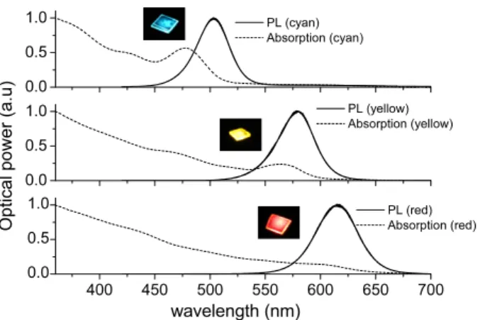
Figure 1. Photoluminescence (PL) and absorption spectra of our CdSe/ZnS core–shell nanocrystals in thin films at room temperature.
enables the color properties of the resulting emission such as tristimulus coordinates, correlated color temperature and color rendering index to be controlled and adjusted.
For white light generation, we use CdSe/ZnS core–shell nanocrystals of crystal sizes 1.9, 3.2 and 5.2 nm (with a size distribution of ±5%) from Evident. The emission colors of these nanocrystals are cyan, yellow and red, tuned using the quantum size effect across the visible spectral range with their corresponding photoluminescence (PL) peaks at 504 nm, 580 nm and 615 nm, respectively. These nanocrystals have high PL quantum yields ranging between 30 and 50%. Such core–shell NCs are shown to yield even higher efficiencies up to 66% [12]. We used similar types of nanocrystals in our previous work for white light sources integrated on blue nitride LEDs [6, 7] and nanocrystal-based UV scintillators integrated on Si detectors [13]. In this work, we prepare high-concentration NC solutions to vortex-mix into the host polymer of poly(methyl-methacrylate) (PMMA). We evaporate NC films in micro-droplets of 25μl by drop-casting at 70–100◦C for optimal film formation and complete the polymerization process for each layer in the assembly. Figure 1shows the photoluminescence and absorption spectra of our CdSe/ZnS core–shell nanocrystals in thin films of the host PMMA.
We use InGaN/GaN-based LEDs with a peak wavelength of 383 nm in the near-ultraviolet as the pump source for the entire hybrid devices presented in this paper. Figure2shows the design of our LEDs. For epitaxial growth, we use a GaN dedicated metal–organic chemical vapor deposition (MOCVD) system. First, we begin with a 14 nm thick GaN nucleation layer. To increase the crystal quality of the subsequent epitaxial layers, we then grow a 200 nm thick GaN buffer layer. For the n-type contact, we grow a 690 nm thick Si-doped epitaxial layer. For the active layers, we continue the epi-growth with five 2–3 nm thick InGaN wells and GaN barriers at a growth temperature of 720◦C. We finish our growth with the p-type layers that consist of a 50 nm thick Mg-doped AlGaN layer and a 120 nm thick Mg-doped GaN layer as the contact cap. Finally, we activate the Mg dopants at 750◦C for 15 min. We used similar growth steps for the development of our GaN-based quantum electroabsorption modulators [14].
Our device fabrication follows standard semiconductor processing procedures as in our previous work [14–16]. These include photolithography, thermal evaporation (metallization), 2
Figure 2. Epitaxial structure of our n-UV LED.
(a) (b)
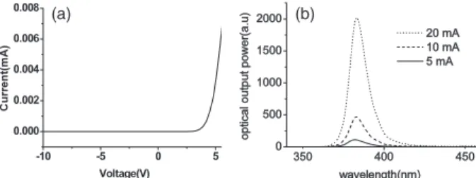
Figure 3. (a) I –V and (b) electroluminescence (EL) spectra (λEL= 383 nm) of our n-UV LEDs under different levels of current injection at room temperature.
reactive ion etch (RIE) and rapid thermal annealing. We use photolithography and reactive ion etching (down to 940 nm) to expose the n-type layer and then apply thermal evaporation to deposit the metal contacts. We form the ohmic p-contacts with metal deposition of 15 nm of Ni with a 100 nm overlayer of Au followed by rapid thermal annealing at 700◦C for 30 s. We lay down a 10 nm layer of Ti with a 200 nm overlayer of Al for the n-contacts followed by a rapid thermal anneal at 600◦C for 1 min under nitrogen. Figure3(a) shows the I–V characteristics of our fabricated n-UV LEDs with turn-on voltages at approximately 5 V and figure3(b) shows their electroluminescence (EL) spectra under different levels of current injection, with the EL peak wavelength at 383 nm. In hybrid devices, this high-energy electroluminescence of the LED excites the integrated NC layers, resulting in spontaneous emission from each NC layer.
In hybrid devices, the electrically driven UV LED optically pumps the NCs and the photoluminescence of these NC layers then collectively generates the white light. For that, we use dichromatic and trichromatic combinations of NCs to be excited by our near-UV LED platform. For the dichromatic combination, we employ cyan and red NCs (λPL = 504 and 615 nm). At first we integrate 650 nm thick cyan-emitting NC film with a 23% volume ratio of the NCs to the host PMMA. On top of this layer, we hybridize 575 nm thick red-emitting NC film with a 13% volume ratio. In our previous work, much thicker NC films (tens of micrometers thick) were required for blue pumping [6,7]. Figure4demonstrates the electroluminescence spectra of this n-UV LED hybridized with the dichromatic nanocrystal combination at various current injection levels. The resulting tristimulus coordinates are
(x, y) = (0.37,0.46)in the near-white region. The correlated color temperature and color rending index areTc = 4520 K and Ra = 43.1. Such operating points were also previously
Figure 4. Electroluminescence spectra of dichromatic combinations of cyan (λPL= 504 nm) and red (λPL= 615 nm) nanocrystals hybridized on an n-UV LED for various current levels at room temperature.
Figure 5. Electroluminescence spectra of trichromatic combinations of cyan (λPL= 504 nm), yellow (λPL= 580 nm) and red
(λPL= 615 nm) emitting nanocrystals hybridized on an n-UV LED for various current levels at room temperature.
obtained using blue LED pumps, e.g. in [17,18]. However, because of the dichromaticity, the color rendering index is low here. To improve the white light quality, we work with triple combinations of NCs next.
For hybridizing trichromatic combinations of NCs, we use cyan, yellow and red NCs (λPL = 504, 580 and 615 nm) on an n-UV LED. We integrate NC films of 650 nm in thickness each with a 23% NC-to-host volume ratio in the assembly, in the order cyan, yellow and red from bottom to top. Figure5
shows the electroluminescence spectra of integrated white LEDs with triple NC combinations at various current injection levels. These spectra correspond to x = 0.38, y = 0.48,
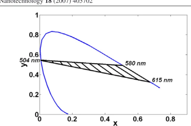
Tc=4434 K andRa =67.6. In this case, the color rendering index is significantly improved compared to the dichromatic combination. Here it is worth noting that these WLEDs, which consist of the dual and triple NC combinations pumped by n-UV excitation LEDs, are improved in terms of color rendering indices also when compared to our previous work using blue LED pumps [6, 7]. The CdSe/ZnS NCs available at our labs cover the visible spectrum from cyan (504 nm) to red (615 nm); their possible combinations are thus confined within the shaded region of the color chromaticity diagram shown in figure 6. One future direction of our research work is to expand this shaded region to include the center of the white region (∼0.33,
Nanotechnology 18 (2007) 405702 S Nizamoglu and H V Demir
Figure 6. Color gamut covered using cyan, yellow and red CdSe/ZnS nanocrystals in the C.I.E. color chromaticity diagram.
Table 1. Summary of the optical characteristics of our hybrid NC-LED sources.
Nanocrystal combination x y Tc(K) Ra Double (cyan and red) 0.37 0.46 4529 43.1 Triple (cyan, yellow and red) 0.38 0.48 4434 67.6
∼0.33) using nanocrystals emitting at <490 nm to further improve the white light quality. Table1presents a summary of the optical characteristics of our hybrid NC–LED sources.
In conclusion, we have presented the design, growth, fabrication, integration and characterization of alternative hybrid white light sources that rely on the layer-by-layer assembly of dichromatic and trichromatic CdSe/ZnS core– shell nanocrystal emitters on InGaN/GaN LEDs developed for pumping at 383 nm in the near-UV spectral range. Here the layer-by-layer hybridization of nanocrystals provided the ability to precisely control individual nanocrystal film thicknesses and order in addition to nanocrystal concentrations. By utilizing multiple combinations of nanocrystals in the assembly, the optical properties of the resulting photoemission are well controlled and adjusted. In this work, the hybrid light sources required much thinner NC films (hundreds of nanometers thick) in the case of UV pumping than for the NC films (tens of micrometers thick) required for blue pumping in our previous work. Using ordered layers of such thin nanocrystal films, higher color rendering indices were obtained with UV pumping when compared to the results of dual and triple NC combinations used with blue pumping in our previous work.
In such UV-based hybrid light sources, the hybridized semiconductor nanocrystals are pumped efficiently and virtually all of the visible emission originates from these nanocrystals to contribute collectively to the white light generation. Given the UV technology roadmap, UV LEDs will provide high power excitation platforms to pump the
nanocrystals on a chip. As a result of our proof-of-concept demonstration in this work we believe that these hybrid UV WLEDs are promising candidates for future solid-state lighting applications.
Acknowledgments
This work is supported by EU-PHOREMOST Network of Excellence 511616 and Marie Curie European Reintegration Grant MOON 021391 within the 6th European Community Framework Program and TUBITAK under project nos. EEEAG 106E020, 104E114, 105E065 and 105E066. HVD and SN also acknowledge additional support from the Turkish National Academy of Sciences Distinguished Young Scientist Award and TUBITAK Fellowship programs.
References
[1] Arik M, Petroskf J and Weavery S 2002 Inter Society Conf. on Thermal Phenomena pp 112–20
[2] Schubert E F 2006 Light-Emitting Diodes (Cambridge: Cambridge University Press)
[3] Nakamura S and Fasol G 1997 The Blue Laser Diode (Berlin: Springer)
[4] Yamada M, Narukawa Y, Tamaki H, Murazaki Y and Mukai T 2005 IEICE Trans. Electron.E88–C 9 1860–71 [5] Heliotis G, Gu E, Griffin C, Jeon C W, Stavrinou P N,
Dawson M D and Bradley D D C 2006 J. Opt. A: Pure Appl. Opt.8 445–9
[6] Nizamoglu S, Ozel T, Sari E and Demir H V 2007 Nanotechnology18 065709
[7] Nizamoglu S, Ozel T, Sari E and Demir H V 2006 IEEE COMMAD Conf. on Optoelectronic and Microelectronic Materials and Devices (Perth) WO-A5
[8] Chen H, Yeh D, Lu C, Huang C, Shiao W, Huang J, Yang C C, Liu I and Su W 2006 IEEE Photon. Technol. Lett.
18 1430–2
[9] Chen H, Hsu C and Hong H 2006 IEEE Photon. Technol. Lett. 18 193–5
[10] Sandhu A 2007 Nat. Photon.1 38
[11] Ali M, Chattopadhyay S, Nag A, Kumar A, Sapra S, Chakraborty S and Sarma D D 2007 Nanotechnology 18 075401
[12] Talapin D V, Rogach A L, Kornowski A, Haase M and Weller H 2001 Nano Lett.1 207–11
[13] Mutlugun E, Soganci I M and Demir H V 2007 Opt. Express 15 1129
[14] Sari E, Nizamoglu S, Ozel T and Demir H V 2007 Appl. Phys. Lett.90 011101
[15] Sabnis V A, Demir H V, Fidaner O, Harris J S, Miller D A B, Zheng J F, Li N, Wu T C, Chen H T and Houng Y M 2004 Appl. Phys. Lett.84 469–71
[16] Demir H V, Sabnis V A, Zheng J F, Fidaner O, Harris J S and Miller D A B 2004 IEEE Photon. Technol. Lett.16 2305–7 [17] Chen C H, Chang S J, Su Y K, Sheu J K, Chen J F, Kuo C H
and Lin Y C 2002 IEEE Photon. Technol. Lett.14 908–10 [18] Chen W R and Huang C J 2004 IEEE Photon. Technol. Lett.
16 1259–61