Developing a Transducer Based on Localized Surface Plasmon
Resonance (LSPR) of Gold Nano Structures for Nanobiosensor
Applications
Adil B. Turhan
1, Demet Ataman
2, Semih Çakmakyapan
1, Mehmet Mutlu
2and Ekmel Özbay
1,3,41
Bilkent University, Nanotechnology Research Center (NANOTAM), Ankara, Turkey
2
Hacettepe University, Institute for Pure and Applied Sciences, Plasma Aided Bioengineering and Biotechnology (PABB) Research Group, Ankara, Turkey
3
Bilkent University, Department of Physics, Ankara, Turkey
4
Bilkent University, Department of Electrical and Electronics Engineering, Ankara, Turkey
Keywords: LSPR, electron beam lithography, plasma polymerization, transducer, biosensor,
electromagnetic simulation, FDTD.
Abstract. In this work, we report the nanofabrication, optical characterization, and electromagnetic
modeling of various nanostructure arrays for localized surface plasmon resonance (LSPR) based biosensing studies. Comparison of the experimental results and simulation outputs of various nanostructure arrays was made and a good correspondence was achieved.
Introduction
Localised surface plasmon resonance (LSPR) of metallic nano structures is a phenomenon that is being researched on and used for biosensor applications intensively [1-5].
Surface plasmon resonance is the coherent oscillation of the surface conduction electrons excited by electromagnetic radiation [6]. It is observable in materials with negative real and near-zero imaginary dielectric constant. For the case of localized surface plasmons, light interacts with particles much smaller than the incident wavelength, which leads to a plasmon that oscillates locally around the nanoparticle with a certain resonance frequency [7,8]. This electromagnetic field enhancement provides high sensitivity to the changes in refractive index, which can be used as a transducer mechanism for biosensors.
Scattering of light from spherical nanostructures and thus the extinction spectrum resulted from LSPR phenomenon of such structures can be explained by the Mie solution to Maxwell’s equations [9]. Extinction (sum of scattering and absorption) intensity, is given as:
= / − (Eq.1) where is the extinction wavelength, is the areal density, r is the radius of the nano spheres, ! is the dielectric constant of the surrounding medium, and " are the real and imaginary parts of the metallic nano spheres’ dielectric function. #, is a variable whose value depends on the aspect ratio and shape of the nanostructures.
As it can be interpreted from equation 1; resonance wavelength, the amount of resonance wavelength shift due to the change of the local refractive index, maximum achievable sensitivity, detection limit and such other important parameters about possible biosensing applications are related to the material used, size and shape of the nano particles [10-14] and period of structure array [15,16].
There are various ways to fabricate nanostructures for LSPR applications. But the lithographic techniques provide precise control over the nanostructure parameters mentioned above which are the key properties to tune and optimize the application for specific purposes. In this study, we have used electron beam lithography for the nano patterning of the plasmonic structures which is a sophisticated nano engineering tool that provides a great ability to thoroughly engineer the nanostructures [17].
Key Engineering Materials Vol. 543 (2013) pp 393-401 © (2013) Trans Tech Publications, Switzerland doi:10.4028/www.scientific.net/KEM.543.393
Fabricated structures were inspected by using a scanning electron microscope. The measurements of nanoparticle LSPR spectra were done by transmission spectroscopy.
Recently, we were able to use plasma polymerization technique successfully for the surface modification of these gold nanostructures [18]. In this process, we employed ethylenediamine as a precursor to incorporate amino groups to the surface. After chemical treatment with bifunctional cross-linker, glutaraldehyde, avidin molecules were immobilized on the surface to form a biological recognition layer which provided binding sites for the biotin molecules that were chemically introduced to the surface afterwards. We were able to observe the expected redshift of the resonance wavelength which proves the usability of this transducer system as a biosensor.
In this study, we worked on electromagnetic simulations for LSPR response of various nanostructure designs. We used finite-difference time-domain (FDTD) method, which is a widely used time domain numerical simulation technique.
Materials and Methods
Gold nanostructures were fabricated over sapphire substrates. A PMMA electron beam resist layer of about 180 nm was spin coated on the samples and was hard baked at 180°C for 90 s. A water soluble conducting polymer (commercially known as aquaSAVE) was also spin coated on top of resist layer to avoid charging during electron beam lithography. e_LiNE plus system of Raith GmbH was used for electron beam lithography. A write field of 100 µm2, an aperture of 20 µm and an acceleration voltage of 10 kV was used. Beam current was around 90 pA. Dot exposure mode was used and applying a range of exposure doses for each design enabled us to obtain targeted nano disk radii. Resist development was done with MIBK:IPA (1:3) for 40 s. Following the electron beam lithography, metal coatings with various thicknesses were done by electron beam evaporation method and the nanostructure arrays were formed after the subsequent lift-off process.
Measurements
Fabricated nanostructure arrays were inspected and their correspondence with the designed dimensions was validated by scanning electron microscopy.
Optical characterization was made by transmission spectroscopy later to be compared with the simulation results. A standart transmission geometry with unpolarized light was used.
Simulations
We used Lumerical Solutions software for our electromagnetic simulations. The effects of nanostructure array parameters such as periodicity and nano disk radius to the LSPR response of the system for both transmission and reflection spectrums were investigated.
Results and Discussion
Simulation results were compared with the transmission spectrums of the fabricated nanostructure arrays.
Fig. 1, An SEM image of one of the fabricated arrays
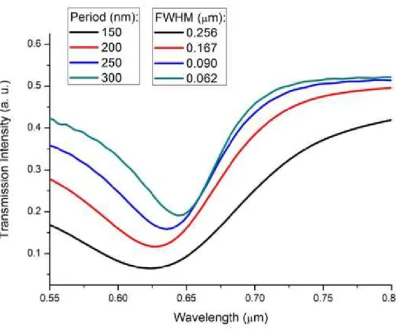
Keeping the radius and the metal thickness constant while increasing the period of the nano disk array gives a red-shifted and narrower resonance curve. Fig. 2 and Fig. 3 shows transmission and reflection spectrums for nano disk arrays with different lattice constants, a radius of 100 nm and a metal thickness of 50 nm. There is a decrease in the extinction intensity with the increasing lattice constant, which is consistent with the direct relationship between the extinction intensity and areal density in Eq. 1. It can also be attributed to the less surface coverage.
Key Engineering Materials Vol. 543 395
Fig. 2, Transmission spectrum simulation of nano disk arrays with different lattice constants, a radius of 100 nm and a metal thickness of 50 nm.
Fig. 4 shows transmission spectrum measured from fabricated nano disk arrays with different lattice constants, a radius of 70 nm and a metal thickness of 50 nm. Results are consistent with the simulation outputs.
Fig. 4, Transmission spectrum measured from fabricated nano disk arrays with different lattice constants, a radius of 70 nm and a metal thickness of 50 nm.
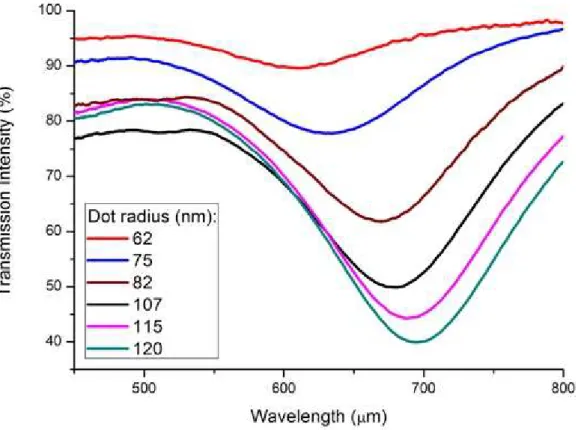
Fig. 5 and Fig. 6 shows transmission and reflection spectrums for nano disk arrays with different radii, a lattice constant of 300 nm and a metal thickness of 50 nm. Keeping the lattice constant and the metal thickness constant while increasing the radius of the nano disks gives a red-shifted and wider resonance curve. There is an increase in the extinction intensity with the increasing lattice constant, which is again consistent with Eq. 1 and again can also be attributed to the less surface coverage.
Key Engineering Materials Vol. 543 397
Fig. 5, Transmission spectrum for nano disk arrays with different radii, a lattice constant of 300 nm and a metal thickness of 50 nm.
Fig. 7 shows transmission spectrum measured from fabricated nano disk arrays different radii, a lattice constant of 300 nm and a metal thickness of 50 nm. Results are consistent with the simulation outputs. Results are very consistent with the simulation outputs.
Fig. 7, Transmission spectrum spectrum measured from fabricated nano disk arrays different radii, a lattice constant of 300 nm and a metal thickness of 50 nm.
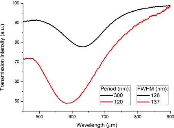
Although the experimental results followed the same trend as the simulation data, main influences on the slight dissimilarity is thought to be fabrication based factors such as the degree of inhomogeneity or the amount of deviation from the designed structures. Nevertheless, we were able to obtain very strong agreements too as it is shown in Fig. 8.
Key Engineering Materials Vol. 543 399
Fig. 8, Simulation data and measurement result for transmission spectrum of a nanostructure array with a radius of 70 nm, metal thickness of 50 nm and a period of 300 nm
Conclusion
In our study, cylindrical nanostructure arrays having different sizes and periodicity were fabricated, their transmission spectrum was measured and compared to the electromagnetic simulations run for these designs by using finite-difference time-domain method. Simulation data and experimental results were highly correlated, which is very promising for optimization of these nano structure arrays for biosensor applications as having a resonance curve with a narrow bandwith and a deep depth would certainly increase sensitivity.
References
[1] C. R. Yonzon, E. Jeoungf, S. L. Zou: Journal of the American Chemical Society, 126(39), 12669-12676 (2004).
[2] A. J. Haes, W. P. Hall, L. Chang et al.: Nano Letters, 4(6), 1029-1034 (2004).
[3] A. J. Haes, L. Chang, W. L. Klein et al.: Journal of the American Chemical Society, 127(7), 2264-2271 (2005).
[4] M. P. Kreuzer, R. Quidant, G. Badenes et al.: Biosensors & Bioelectronics, 21(7), 1345-1349 (2006).
[5] M. Vestergaard, K. Kerman, D. K. Kim et al.: Talanta, 74(4), 1038-1042 (2008). [6] E. Ozbay: Science, 311(5758), 189-93 (2006).
[7] K. A. Willets, and R. P. Van Duyne: Annual Review of Physical Chemistry, 58, 267-297 (2007).
[8] J. N. Anker, W. P. Hall, O. Lyandres et al.: Nature Materials, 7(6), 442-453 (2008). [9] G. Mie: Ann. Phys., 25(377), (1908).
[10] A. D. McFarland, R.P. Van Duyne: Nano Letters, 3(8), 1057-1062 (2003).
[11] L. J. Sherry, S. H. Chang, G. C. Schatz et al.: Nano Letters, 5(10), 2034-8 (2005).
[12] T. R. Jensen, C. L. Haynes, R. P. Van Duyne: J. Phys. Chem. B, 104(45), 10549–10556 (2000).
[13] J. J. Mock JJ, D. R. Smith, D. A. Schultz, S. Schultz: J. Chem. Phys. , 116(6755), (2002). [14] J. J. Mock, S. Schultz: Nano Letters, 3(4), 485–491 (2003).
[15] W. Rechberger, A. Leitner, J.R. Krenn, B. Lamprecht, F. R. Aussenegg FR: Optics Communications, 220(1-3), 137-141 (2003).
[16] K. H. Su, X. Zhang, J.J. Mock, D. R. Smith, S. Schultz: Nano Letters, 3(8), 1087-1090 (2003).
[17] G. Barbillon, J. Plain, M. L. De la Chapelle, P.M. Adam, P. Royer: Surface Science, 601, 5057–5061 (2007).
[18] Submitted for Publication, A. B. Turhan, D. Ataman, Y. Sen, M. Mutlu, E. Ozbay: Journal of Nanophotonics (2012)
Key Engineering Materials Vol. 543 401