NOVEL MINIATURIZED SENSORS FOR
ON-SITE BIOLOGICAL AND CHEMICAL
DETECTION
a dissertation submitted to
the graduate school of engineering and science
of bilkent university
in partial fulfillment of the requirements for
the degree of
doctor of philosophy
in
materials science and nanotechnology
By
Hasan G¨
uner
NOVEL MINIATURIZED SENSORS FOR ON-SITE BIOLOGICAL AND CHEMICAL DETECTION
By Hasan G¨uner August 2016
We certify that we have read this dissertation and that in our opinion it is fully adequate, in scope and in quality, as a dissertation for the degree of Doctor of Philosophy.
Aykutlu Dana(Advisor)
Ali Kemal Okyay
Mehmet ¨Ozg¨ur ¨Oktel
Adil Denizli
Hamza Kurt
ABSTRACT
NOVEL MINIATURIZED SENSORS FOR ON-SITE
BIOLOGICAL AND CHEMICAL DETECTION
Hasan G¨uner
Ph.D. in Materials Science and Nanotechnology Advisor: Aykutlu Dana
August 2016
The development of miniaturized analytical systems brought several examples of novel platforms for a variety of applications in medical diagnostics, food safety, biodefense, agricultural and environmental monitoring. Portability, sensitivity, reliability, short turn-around-time, cost-efficiency and connectivity are some of the critical assets that successful devices should possess. The advancements in such areas enabled the detection and analysis of biological and chemical agents outside the laboratory settings. In this thesis, we focus on the development of miniaturized sensor designs for on-site biological and chemical detection utiliz-ing surface plasmon resonance sensutiliz-ing and infrared absorption spectroscopy. We proposed an integrated refractometric sensor combining a grating-coupled plas-mon resonance surface with a planar photodiode which can find applications in lab-on-a-chip designs with high integration density. In order to address the use of lab-on-a-chip systems in point-of-care testing applications, we have developed a surface plasmon resonance imaging platform integrated with a smartphone. We have fabricated low cost and sensitive grating coupled surface plasmon resonance sensor chips using off-the-shelf optical storage discs. Then we have experimen-tally shown the capability of multiplexed detection and biomolecular sensing. Finally, we demonstrated infrared absorption spectroscopy on a mobile phone by developing a compact mid-infrared spectrometer that hosts a miniature uncooled thermal camera and a custom-designed silicon transmission diffraction grating.
¨
OZET
YER˙INDE B˙IYOLOJ˙IK VE K˙IMYASAL TAY˙IN˙INE
Y ¨
ONEL˙IK YEN˙I M˙INYAT ¨
UR ALGILAYICILAR
Hasan G¨uner
Malzeme Bilimi ve Nanoteknoloji, Doktora Tez Danı¸smanı: Aykutlu Dana
A˘gustos 2016
Minyat¨ur analitik sistemlerdeki geli¸smeler, tıbbi tanı, gıda g¨uvenli˘gi, biyosavunma, zırai ve ¸cevresel tarama uygulamalarına y¨onelik yeni platformları beraberinde ge-tirdi. Bu ba˘glamdaki ba¸sarılı bir cihazdan beklenen ba¸slıca nitelikler arasında ta¸sınabilirlik, hassasiyet, g¨uvenilirlik, kısa s¨urede sonu¸c t¨uretebilme, maliyet avantajı ve ba˘glanabilirlik ¨ozellikleri sayılabilir. Bu alanlardaki ilerlemeler sayesinde biyolojik ve kimyasal ajanların laboratuvar ko¸sulları dı¸sında tayin ve analizinin m¨umk¨un hale geldi˘gi g¨or¨ulmektedir. Bu ¸calı¸smada, yerinde biyolo-jik ve kimyasal tayinine y¨onelik, y¨uzey plazmon rezonansı algılama ve kızıl¨otesi emilim spektroskopisine dayalı minyat¨ur algılayıcı tasarımları ¨uzerine odaklandık. Kırınım a˘gı e¸slemeli y¨uzey plazmon rezonansı y¨uzeyiyle d¨uzlemsel bir fotodiyotu birle¸stirerek t¨umle¸sik refraktometrik algılayıcı geli¸stirdik. Bu algılayıcı mekaniz-masının y¨uksek t¨umle¸stirme yo˘gunluklu yonga ¨ust¨u laboratuvar tasarımlarında uygulama alanı bulması ¨ong¨or¨ulmektedir. Yonga ¨ust¨u laboratuvar sistemlerinin hasta ba¸sı tarama uygulamalarında kullanımına katkı sa˘glama amacıyla, akıllı telefon tabanlı bir y¨uzey plazmon rezonansı g¨or¨unt¨uleme platformu geli¸stirdik. Optik veri disklerini kullanarak d¨u¸s¨uk maliyetli ve hassas kırınım a˘gı e¸slemeli y¨uzey plazmon rezonansı algılayıcı ¸cipleri ¨urettik. Sistemin ¸coklu okuma ve biy-omolek¨uler algılama performansını deneysel olarak ortaya koyduk. Son olarak, cep telefonuyla kızıl¨otesi emilim spektroskopisi ¨ol¸c¨um¨u yapabilen, minyat¨ur bir so˘gutmasız termal kamera ve ¨ozel tasarlanan silikon ge¸cirgenlik kırınım a˘gını barındıran kompakt bir orta-kızıl¨otesi spektrometresi geli¸stirdik.
Anahtar s¨ozc¨ukler : Minyat¨ur algılayıcılar, analitik sistemler, yonga ¨ust¨u lab-oratuvar aygıtlar, y¨uzey plazmon rezonansı algılama, kızıl¨otesi emilim
spek-Acknowledgement
I would like to express my sincere gratitude to my academic advisor Assist. Prof. Aykutlu Dana for his tremendous support, guidance, encouragement, un-derstanding and patience. It has been a great honor for me to be a part of his research group and complete my Ph.D. degree under his supervision at UNAM-National Nanotechnology Research Center.
I would like to thank Assist. Prof. Ali Kemal Okyay and Assoc. Prof. Mehmet ¨
Ozg¨ur Oktel for their valuable suggestions and comments throughout this thesis study.
I would like to thank Prof. Adil Denizli and Prof. Hamza Kurt for accepting to be a part of my thesis committee and taking their valuable time to evaluate my dissertation.
I am very much thankful to Assist. Prof. C¸ a˘glar Elb¨uken for his invaluable support and collaboration. I have learnt a lot from him not only in the academic sense but also in terms of personality traits.
I particularly thank Dr. Erol ¨Ozg¨ur for being such a great teammate and for his unrequited help.
I owe special thanks to the members of T ¨UB˙ITAK B˙ILGEM Bioelectronics Devices and System Development Group; Dr. Yıldız Uluda˘g, G¨uzin K¨okt¨urk, Elif Esen and Mehmet Ya˘gmur G¨ok for their cooperation and contributions.
I feel fortunate to work and discuss with many of my colleagues especially Dr. Burak T¨urker, Mehmet C¸ elik, Gamze Toruno˘glu, Dr. Sencer Ayas, Ahmet Emin Topal, Hepi Hari Susapto, Dr. Mehmet Kanık, Mustafa Tahsin G¨uler, Merve Mar¸calı, Pelin K¨ubra ˙I¸sg¨or, ˙Ismail Bilican, Fahri Emre ¨Ozt¨urk, Assist. Prof. G¨okhan Bakan, Nihat Serkan Karayal¸cın, Mustafa ¨Urel, Murat Serhatlıo˘glu, Dr. Ozan Akta¸s, Dr. Ruslan Garifullin, Mehmet Girayhan Say and Ziya I¸sıksa¸can.
I want to express my special thanks to present and former UNAM staff; Mustafa G¨uler, Semih Ya¸sar, Hakan S¨urel, Berk Berkan Turgut, Halil Volkan
vi
I am grateful to my dear friends Mustafa Kemal ˙I¸sen, Sinan G¨undo˘gdu, U˘gur Karata¸s, Tu˘gba ˙I¸sen, Sercan C¸ ayır, Berkay ¨Ulk¨u, Durali ˙Ipek and G¨ul¸sen G¨ozbulut for their sincere companionship and motivation during the tough times of this work.
I appreciate the moral support of my lifelong friends Osman Pamuk, Mevl¨ut Akdeniz, Serkan Sonel, Murat Ak, Ali Cevahir and H¨useyin G¨okhan Ak¸cay.
I would like to acknowledge The Scientific and Technological Research Council of Turkey, T ¨UB˙ITAK, for Ph.D. scholarship and project grants.
And of course, I would like to express my sincere gratitude to my parents and sisters for their endless support and unconditional love. I dedicate this work to my smart nephew Kaan Aydeniz.
Contents
1 Introduction 1
1.1 Organization of the thesis. . . . 2
2 Grating Coupler Integrated Photodiodes for Plasmon Resonance Based Sensing 4
2.1 Introduction . . . . 5
2.2 Theoretical aspects of grating coupling to the plasmon mode and estimation of SPR sensitivity . . . . 7
2.3 Experimental . . . 10
2.3.1 Photodiode substrate fabrication . . . . 12
2.3.2 Nano-imprinted mold fabrication . . . .14
2.3.3 Measurements . . . . 15
2.4 Results and discussion . . . . 15
2.4.1 Grating profiles . . . .15
2.4.2 Plasmon resonance characteristics and sensitivity . . . . 17
2.4.3 Discussion . . . . 19
2.5 Conclusion . . . . 21
3 A smartphone based surface plasmon resonance imaging (SPRi) platform for on-site biodetection 22
3.2.1 Smartphone attachment for surface plasmon resonance imaging. 26
3.2.2 Design and fabrication of SPRi sensor chips. . . .29
3.2.3 Measurement protocol. . . . 41
3.2.4 Experimental setup for wavelength interrogation of plasmon resonance. . . . 43
3.2.5 Optimization of the illumination wavelength. . . . 46
3.2.6 Chemical materials. . . . 48
3.3 Results and discussion. . . . 49
3.3.1 Microarray imaging of Ag/Au bimetallic sensing spot. . . . 49
3.3.2 Real-time monitoring of bovine serum albumin (BSA) adsorption . . . . 53
3.3.3 Demonstration of a biodetection assay. . . 57
3.4 Conclusion. . . 59
4 Infrared absorption spectroscopy on a mobile phone 61
4.1 Introduction. . . 61
4.2 Materials and Methods. . . . 62
4.2.1 Spectrometer configuration for IR absorption spectroscopy. . .62
4.2.2 Uncooled thermal cameras as photodetector arrays. . . . 63
4.2.3 Silicon transmission diffraction grating. . . .64
4.2.4 Experimental setup. . . .67
4.3 Results and Discussion. . . . 68
4.4 Conclusion. . . .71
5 Conclusion 72
Bibliography 76
List of Figures
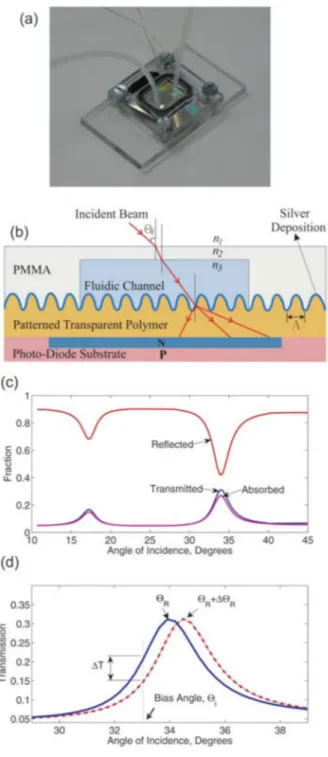
Figure 2.1: (a) Photograph of the sensor device with a PMMA fluidic chamber and in/outlet tubing. (b) Cross-sectional schematic view of the device structure. (c) Simulation results of the reflection, transmission and absorption data for TM polarization in the case of a 30 nm deep sinusoidal grating, deposited with a 45 nm thick Ag layer and illuminated by a 632.8 nm light source. The working medium is water with 𝑛𝑑= 1.33. (d) The operational principle of the device is
schematically shown. The illumination is kept at a fixed angle Θ𝑖 and a small
perturbation (δΘ𝑅) of the resonance condition (Θ𝑅) results in a change (δT) in the
transmitted intensity. ………...11
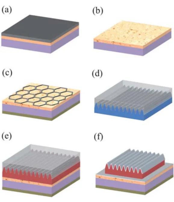
Figure 2.2: Fabrication steps of a grating coupler-integrated photodiode ((a)–(f)). (a) n-type Si wafer, amorphous Si, aluminum (from bottom to top). (b) Amorphous Si is aluminum doped during thermal curing. (c) Contact pads on top-side are patterned by lithography of an additionally deposited Al layer. Photodiode substrate is completed by the deposition of gold–palladium at the bottom-side to form the contact pads. (d) Grating profile is replicated from a surface modified DVD disc. PDMS is poured on the master mold and cured at 70 oC for 5 h. Cured
PDMS is peeled off from the master mold and used as elastomeric stamp. (e) Photoresist polymer is spin-coated on the photodiode substrate. Elastomeric stamp is released gently on the polymer film and hard-baked. Stamp is mechanically removed from the sample. (f) Contact mask is defined by the optical lithography.
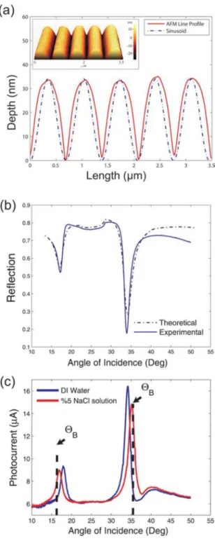
Figure 2.3: (a) AFM line profile of the grating structure with a depth of 35 nm is depicted compared to a sinusoidal grating profile. Inset figure illustrates AFM topography of the corresponding grating structure with a groove depth of 35 nm and 45 nm thick silver coating. (b) Reflection behavior of the grating structure is depicted in water medium under incidence of a 632.8 nm wavelength light source. Solid lines show the reflection measurement results whereas the dashed lines show theoretical results. (c) Measured photocurrent response of the integrated sensor as a function of the angle of incidence for water and NaCl solution. Bias angles used in the time-resolved measurements are shown by arrows……….16
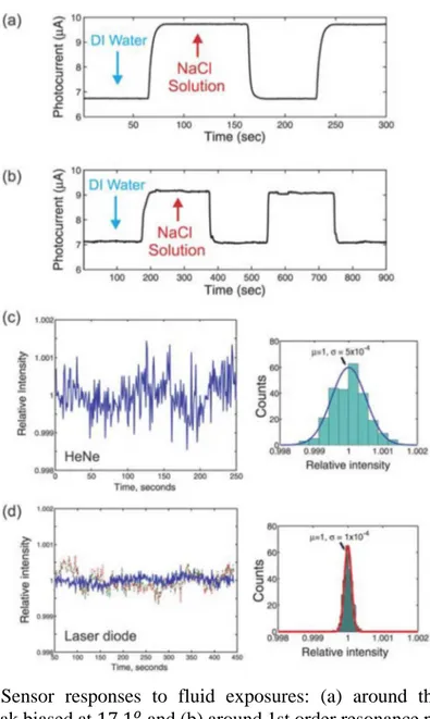
Figure 2.4: Sensor responses to fluid exposures: (a) around the 2nd order resonance peak biased at 17.1𝑜 and (b) around 1st order resonance peak biased at
35.6𝑜 respectively. A 632.8 nm HeNe laser source is used, resulting in an
equivalent refractive index noise of 6.3 x 10⁻⁶ 𝑅𝐼𝑈/√𝐻𝑧. (c) Stability of the measurement set-up using a 2 mW HeNe source and (d) using a power stabilized 650 nm laser diode. Further noise reduction is demonstrated using balanced detection. In (d) a reference photodiode monitors the light intensity at the source while the device is biased near the first order resonance. Normalized intensities for the reference diode (dotted) and SPR diode (dashed) are shown as well as the ratio of the two (solid). In the balanced measurement, the SPR intensity signal can be measured with a 0.01 %/√𝐻𝑧 relative intensity noise. Resulting detection noise floor is 1.2 x 10⁻⁶ 𝑅𝐼𝑈/√𝐻𝑧. Histograms of current readings are shown with corresponding Gaussian curve fits………18
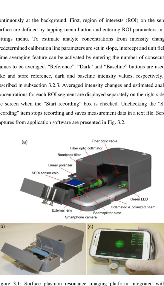
Figure 3.1: Surface plasmon resonance imaging platform integrated with a smartphone. (a) Schematic illustration and (b) photograph of the imaging apparatus. (c) Custom developed smartphone application for real-time and on-site monitoring of multiple sensing spots………27
Figure 3.2: Smartphone application software. (a) When the app is started, zoomed in view of the imaging spot is displayed at the background overlaid by “Button
menu” at the bottom, and “Report table” at the top right corner. (b) “Control menu” pops up at the bottom right corner when the menu button of the smartphone is tapped. (c) Region of interest (ROI) parameters are defined in the “Settings menu”. (d) ROI frames are overlaid on the imaging spot. (e) Other input values like calibration line parameters and number of averaging frames are entered in the “Settings menu”. (f) Following the measurement of reference, dark and baseline intensities by using the buttons in the “Buttons menu”, actual measurement is initiated by checking the “Start record” item in the “Control menu”, and averaged intensity change and estimated analyte concentrations for each ROI are updated separately in the “Report table”. Measurement data is automatically saved in a text file when the recording is stopped by unchecking the “Start record” item………28
Figure 3.3: (a) AFM micrograph of Blu-ray disc surface and (b) line profile……29
Figure 3.4: Calculated reflectance spectra of various types of metallized optical discs under normal incidence of illumination in water medium. Grating periods of Blu-ray Disc (BD), Digital Versatile Disc (DVD) and Compact Disc (CD) are 320
nm, 740 nm and 1.6 m, respectively………...30
Figure 3.5: Calculated SPR reflectance spectra of Ag coated BD chip under normal incidence of illumination in water medium with respect to decreasing silver thickness. As the thickness of silver layer reduces below 80 nm, SPR curve loses its sharpness due to the interaction of surface plasmon wave with the underlying substrate layer………32
Figure 3.6: Change in SPR reflectance spectra of Ag/Au bimetallic BD chip with respect to increasing top gold layer thickness from 2 nm to 10 nm. (a) Calculated and (b) measured reflectance spectra in water medium at normal incidence. Measurements are taken using normal incidence SPR spectroscopy setup……...33
Figure 3.7: Grating coupled SPRi sensor chip. (a) Schematic of the SPRi chip assembly fabricated by integrating a bimetallic Blu-ray disc chip and a disposable fluidic channel. (b) Cross-section schematic view and (c) SEM image of a bimetallic BD chip. Groove depth, d is 20 nm, and pitch width, is 320 nm. Film thicknesses of Ag and Au layers are 80 nm and 2 nm, respectively………...34
Figure 3.8: Integration of a BD sensor chip with a low-cost microfluidic channel fabricated by laser cutting of transparent acrylic plate and double side adhesive tape. (a) Channel geometry is defined on a double-side adhesive tape using a high power CO2 laser cutting system. (b) Inlet and outlet holes with conical profile are
defined on a 3 mm thick transparent acrylic plate again by laser cutting. (c) First, DST is bond onto the milled acrylic plate. (d) Then, acrylic plate and BD chip are bond together tightly by applying mechanical pressure. Inlet and outlet tubings are mount to the device………...36
Figure 3.9: 3D printing based fabrication of a flow cell and integration with a BD sensor chip. (a) Flow cell body is designed by a CAD tool and fabricated using a commercial 3D printer out of a PLA filament. (b) Top surface of the flow cell is rubbed with a sandpaper. (c) BD sensor chip is attached with glue inside the channel. A coverglass is bond using UV curable epoxy under UV exposure. (d) Injector needles as inlet and outlet ports are attached to the channel in the same manner with coverglass bonding………..37
Figure 3.10: PDMS replication molding based fabrication of a flow cell integrated BD chip. (a) SU-8 photoresist is spin-coated on a Si substrate and soft baked on a hotplate. (b) Microchannel geometry is patterned on SU-8 coating by optical lithography followed by post baking and development processes. (c) PDMS-curing agent mixture is poured onto the SU-8 master mold and cured on a hotplate. (d) Hardened elastic PDMS stamp is peeled off gently and treated by air plasma to form hydroxyl groups on the bonding surface. (e) Thin SiO2 film is deposited
(PECVD). (f) Hydroxyl groups are formed on the SiO2 layer by the same air
plasma treatment procedure. (g) Ge (3 nm), Ag (80 nm) and Au (2 nm) films are deposited on Blu-ray disc substrate using thermal vacuum evaporation through a shadow mask. (h) PDMS microchannel is bond with Blu-ray chip. (i) Photograph image of a fabricated device. (j) Photograph image taken by measurement setup camera during the liquid flow………...39
Figure 3.11: A typical measurement protocol. (a)-(c) Plug the SPRi chip into the sample holder unit. (d) Set the polarizer to TE mode (taken as normalization reference). (e) Connect inlet port of the chip to an external pump and inject running buffer. (f) As the flow cell is filled with the liquid, use set screws to align the sample if required. (g) Switch the polarization to TM mode. (h) Follow the assay protocol. (i) Intensity changes (decreases in this configuration) as the molecules attach to the sensor surface...42
Figure 3.12: Experimental setup for the wavelength interrogation of plasmon resonance. (a) Schematic representation and (b) photograph of the optical configuration………43
Figure 3.13: Data analysis steps of time-resolved spectral interrogation measurements. (a) Calculation of the normalized reflectance spectrum by taking the ratio of background corrected TM and TE polarized spectra. (b) Spectrogram showing the change in the resonance curve over time. (c) Optimization of the centroid algorithm. (d) Sensorgram generated using centroid method………….45
Figure 3.14: (a) Reflectance spectra of different brands of BD chips, (b) Calculated reflected spectra with respect to angle of incidence of a particular BD chip………...46
increasing concentrations from 1% to 25% v/v. (b) Bulk refractive index sensitivity with respect to the illumination wavelength. Calibration curves for the resonance wavelength shift (c) and intensity change (d) obtained from the wavelength interrogation setup. The experimental spectral bulk refractive index
sensitivity, SBE is found as 356 nm/RIU………..47
Figure 3.16: Microarray imaging of sensing spots under bulk dielectric media with different refractive indices. (a) Green channel view of an RGB image of a microarray of Ag/Au bimetallic sensing spots under 20% v/v glycerol solution environment (Refractive index of glycerol solution, nd:1.3596). (b) 3D
representation of SPRi difference image. Baseline image is taken under pure water medium (Refractive index of pure water, nd:1.335). (c) Line profile of a row of
microspots. (d) Percentage reflectivity change with respect to the refractive index of bulk medium at varying concentrations of glycerol solutions from 1% to 25% v/v. Bulk refractive index sensitivity obtained from linear calibration curve is 485 %/RIU. Error bars denote 2SD of measurements from 16 spots shown in part (a), demonstrating intra-sensor variability………..51
Figure 3.17: Sensorgrams showing average reflectivity changes of individual sensing spots during fluid exposures. The fluidic channel is initially filled with pure water (refractive index of pure water, nd:1.335) and sensor responses are
taken as baseline signals. Then, 20% v/v glycerol solution (refractive index of glycerol solution, nd:1.3596) is injected onto the microarray surface at 50 L/min
flow rate for 50 seconds. Finally, glycerol solution in the channel is replaced with pure water to return into the initial fluidic state. Circular ROIs overlaid on the inset figure denote the locations of 4 sensing spots on the green channel SPR image where R stands for row and C stands for column positions. Video data is recorded at 30 frames/second rate and averaged over 200 consecutive frames….52
Figure 3.18: Real-time monitoring of BSA adsorption onto the gold surface. (a) Arbitrarily defined 4-by-4 rectangular region of interests (96 x 96 m2 each) on
entirely Ag/Au bilayer coated sensor spot image (top) and background corrected SPRi difference image of ROIs (bottom) taken after BSA adsorption. (b) Sensorgram showing average reflectivity change of ROI spots during the implementation of BSA protocol. The inset schematic illustrates binding of BSA molecules on the grating surface. Error bars denote 2SD of measurements from 16 spots. (c) Reflectance spectra taken before and after BSA adsorption using the normal incidence SPR spectroscopy setup………...54
Figure 3.19: Sensorgram of BSA adsorption onto the gold sensor surface monitored by SPR wavelength interrogation setup. The sensorgram response during the association phase (between the injection of BSA solution and PBS buffer wash) is due to the overall resonance shift, ∆𝜆𝑡𝑜𝑡𝑎𝑙 caused by both surface shift, ∆𝜆𝑠𝑢𝑟𝑓𝑎𝑐𝑒 (BSA adsorption) and bulk shift, ∆𝜆𝑏𝑢𝑙𝑘 (refractive index difference
of solutions). Inset figure depicts resonance wavelength difference, ∆𝜆𝑏𝑢𝑙𝑘=0.033
nm following the PBS wash which is due to the small refractive index difference
between BSA and PBS buffer solutions (Δ𝑛 = 93 × 10−6 𝑅𝐼𝑈)………...55
Figure 3.20: Surface modification of Blu-ray disc plasmonic chips. (i) 11-MUDA SAM formed on thin gold film coated chip. (ii) SAM layer is activated by exposing EDC/NHS mixture. (iii) RAM IgG antibody is immobilized on the activated surface by amine coupling chemistry. (iv) Non-reacted NHS esters were capped with ethanolamine solution to block non-specific analyte bindings. (v) Capture of mouse IgG antibodies by RAM Fc immobilized sensor surface……..57
Figure 3.21: Nanomolar level detection of capture of mouse IgG by immobilized layer of RAM IgG (a) Spectral sensorgram showing the immobilization steps of RAM IgG taken by using the normal incidence SPR spectroscopy setup. (b) Dose-response curve for the capture of mouse IgG taken by using SPR imaging platform. The inset schematics illustrate immobilization of RAM IgG (blue
with RAM IgG, respectively. Error bars denote 2SD of measurements from 3 spots……….59
Figure 4.1: (a) Schematic illustration of IR absorption spectroscopy using a miniature uncooled IR camera. (b) Photograph of the 3D-printed spectrometer apparatus………..63
Figure 4.2: (a) AFM micrograph of microfabricated silicon diffraction grating. Groove depth, d=1.6 𝜇𝑚. (b) Diffracted orders for angle of incidence, 𝜃𝑖 = 30𝑜 and grating period, Λ = 20 𝜇𝑚. Only -1st diffraction order is collected by the
camera lens. (c-f) Calculated transmission efficiencies of diffracted orders for varying groove depths (0.5 𝜇𝑚 (blue), 1.0 𝜇𝑚 (green), 1.5 𝜇𝑚 (red), 2.0 𝜇𝑚 (cyan),
2.5 𝜇𝑚 (magenta))………66
Figure 4.3: Photograph of the experimental setup………67
Figure 4.4: (a) Reference, sample, and transmittance spectrum images of polystyrene reference standard. (from left to right) (b) Ground truth FTIR transmittance spectrum of polystyrene reference standard. (c) Agreement between the IR camera and blurred FTIR spectra……...………70
List of Tables
Table 3.1: Comparison of cell phone based SPR biosensors………...60
Table 4.1:Technical specifications of Seek Thermal camera………...64
Chapter 1
Introduction
Miniaturization of analytical devices for on-site or point-of-care applications, utilizing lab-on-a-chip technologies, is currently an extremely active field of research [1], [2]for enabling their use in the field, instead of laboratories with a high amount of investment. In particular, SPR based sensing has become a popular method for quantitative analysis and characterization of biomolecular interactions [3]–[5] since it provides label-free and real-time detection of binding events with high sensitivity. Surface plasmon resonance (SPR) sensors rely on the general principle that perturbations in the refractive index of the media interfacing with a metal surface induce an alteration in the resonance of surface plasmons. In terms of biosensing, this alteration corresponds to interaction of analyte molecules with specific molecular probes residing on the surface of the biosensor. The spatiotemporal characteristics of this interaction could be deciphered by real-time tracking of this alteration in terms of either a shift in angle of incidence or resonant wavelength, or a change in the measured intensity at a constant wavelength or angle [6], [7]. Each measurement possesses their own pros and cons in terms of sensitivity and convenience of the measurement, which is also affected by the configuration of optical coupling
to the plasmonic surface [8]; however, angular or spectral interrogation of SPR signals necessitates bulky and expensive equipment such as fine calibrated goniometers [9], [10] or spectrometers [11]. Intensity interrogation of plasmonic resonances, on the other hand, can be performed by utilizing simple and miniature photodetectors [12], [13], or smart phone cameras [14], [15]. This advantage of intensity based SPR measurement could be utilized in order to develop miniature SPR devices, especially when combined with planar grating based SPR substrates.
1.1
Organization of the thesis
In chapter 2, we present an integrated refractometric sensor combining a grating-coupled surface plasmon resonance surface with a planar photodiode. We introduce a brief theoretical background on grating-coupled SPR sensing and estimation of SPR sensitivity. We describe the working principle of integrated sensor design that utilizes plasmon enhanced transmission as a sensitive refractive index sensing mechanism. Planar photodiode was fabricated using a metal induced crystallization procedure. Grating-coupler was integrated with the photodiode substrate using nanoimprint lithography and thin film metallization processes. Surface topography was characterized by atomic force microscopy (AFM). Angular SPR curves were obtained using both numerical calculations and variable angle spectroscopic ellipsometry (VASE). Sensor responses to refractive index changes were measured in real-time during fluid exposures. Further noise reduction was demonstrated using balanced detection.
In chapter 3, we present a surface plasmon resonance imaging (SPRi) platform integrated with a smartphone for on-site high-throughput biodetection. We demonstrate how to develop a compact optical attachment which converts a
Flow cells in different structure and geometries were fabricated using laser cutting, 3D printing and polydimethylsiloxane (PDMS) replication molding. Spectral SPR properties were investigated using both simulations and custom-built wavelength interrogation SPR setup. SPR images of Ag/Au bimetallic microspot array were taken using the optical apparatus during flow of glycerol solutions with varying refractive indices. Biodetection performance has been tested through monitoring of bovine serum albumin (BSA) adsorption and selective binding of mouse IgG antibody with immobilized rabbit anti mouse (RAM) IgG antibody.
In chapter 4, we demonstrate infrared absorption spectroscopy on a mobile phone using a miniature uncooled thermal camera. We present dispersive spectrometer configuration for mid-IR spectroscopy that utilizes vanadium oxide microbolometer array technology. A custom transmission diffraction grating was designed using a simulation package based on modified integral method (MIM) and microfabricated out of a silicon wafer through UV optical lithography and inductively coupled plasma (ICP) etching processes. IR transmittance spectrum of a polystyrene film was measured within fingerprint region. Measurement results were compared with ground truth spectra taken by Fourier transform infrared spectroscopy (FTIR) system following further data processing including Fast Fourier Transform (FFT) convolution and blind deconvolution methods.
In chapter 5, we introduce a brief summary of our results and achievements.
Chapter 2
Grating coupler integrated photodiodes
for plasmon resonance based sensing
In this chapter, we propose an integrated sensor combining a grating-coupled plasmon resonance surface with a planar photodiode. Plasmon enhanced transmission is employed as a sensitive refractive index (RI) sensing mechanism. Enhanced transmission of light is monitored via the integrated photodiode by tuning the angle of incidence of a collimated beam near the sharp plasmon resonance condition. Slight changes of the effective refractive index (RI) shift the resonance angle, resulting in a change in the photocurrent. Owing to the planar sensing mechanism, the design permits a high areal density of sensing spots. In the design, absence of holes that facilitate resonant transmission of light, allows an easy-to-implement fabrication procedure and relative insensitivity to fabrication errors. Theoretical and experimental results agree well. An equivalent long-term RI noise of 6.3 x 10⁻⁶ /√ is obtained by using an 8 mW He–Ne
laser, compared to a shot-noise limited theoretical sensitivity of 5.61 x 10⁻⁹
incidence. Further sensitivity enhancement using balanced detection and optimal plasmon coupling conditions are discussed.
This chapter was published as “Grating coupler integrated photodiodes for plasmon resonance based sensing” by Burak Turker*1, Hasan Guner*, Sencer
Ayas, Okan O. Ekiz, Handan Acar, Mustafa O. Guler and Aykutlu Dana, in Lab
Chip. 11, 282–287, 2011.
2.1 Introduction
Surface plasmon resonance (SPR) can be exploited as a sensitive refractive index (RI) sensing mechanism and SPR is one of the most common label-free biosensor technologies with a vast variety of applications in biology, food safety, medical diagnostics, agricultural and environmental monitoring [16]. The main concern in the development of SPR is geared toward designing easy to fabricate, cheap and sensitive biosensors with high integration densities. SPR sensors mainly differ in the optical platforms they are based on. Prism couplers [17], [18] result in comparable higher sensitivity values [3] than grating assisted coupling in plasmon resonance excitation. However, the bulky nature of prisms makes them unsuitable for applications in integrated sensing devices. Waveguide couplers [19] employing fibers appear to present the highest degree of miniaturization in SPR sensors, but require expensive high index prisms for the resonant coupling between a surface plasmon and a waveguide mode and suffer from instable sensitivity responses due to deformations in the fiber. Due to their compact size, planarity and stability, grating couplers [20] have benefits in integrated applications. In this work, we present a device that eliminates the traditional far field detection (CCD/CMOS detector) mechanism [21], [22] by using an integrated photodetector design. The device structure is illustrated in Fig. 2.1a and Fig. 2.1b. The detection mechanism works by monitoring the plasmon enhanced
transmission of light through a thin metal grating that acts as the plasmon resonance sensing surface. Integrating the photo-diode substrate below the grating structure enables the planar geometry and compact integrity of the sensor. As in other SPR sensors, the resonant shifts are only affected by the changes of optical properties within the close vicinity of the surface. Transmission of electromagnetic waves through thin metal films via plasmons has been widely studied in the literature [23]. Plasmon enhanced transmission through sub-wavelength holes [24], [25], nano-hole arrays [26], [27], or periodically corrugated metal surfaces [28] have been investigated theoretically and experimentally [29]. Although plasmon enhancement through nano-hole arrays appears to offer agreeable sensitivity, their realization requires fabrication of holes with high uniformity. Despite the localized nature of plasmon modes in such sub-wavelength aperture arrays and resulting sensitivity to refractive index changes, the overall sensitivity of plasmonic sensors also depends on how sharp the resonances are. Due to fundamental relations between the Fourier components of spatial structure of the surfaces and the SPR, it is difficult to achieve sharp and deep resonances using hole arrays in a simple low-cost fabrication process. In contrast, our approach uses a grating to obtain a plasmonic enhancement of transmission through the silver metallized grating structures. Lack of holes in our design simplifies the fabrication procedure and increases repeatability. Utilizing a bi-harmonic grating topography [30]–[32] rather than a sinusoidal one, observation of higher order resonant coupling is also possible in our devices. The bi-harmonic grating structure allows better excitation of the second order resonance [32]–[34] which also produces an enhancement of light transmission. Such multiple resonances allow SPR detection at a fixed angle of incidence (AOI) for multiple different wavelengths.
2.2 Theoretical aspects of grating coupling to the plasmon
mode and estimation of SPR sensitivity
The momentum mismatch between the in-plane wave vector of impinging photons and the wave vector component of the excited surface plasmons disables a natural momentum coupling at planar surfaces. On a smooth planar interface of a metal and a dielectric, the surface plasmon polariton (SPP) wave vector, kSPP, is
found to be always greater than the wave vector of incident light in air, k0, as given
by
= ≥ = (2.1)
where is the permittivity of the metal layer and is that of the dielectric layer (fluid). One of the techniques for satisfying this energy and momentum match condition is to employ grating schemes. The presence of a metal planar surface that is patterned with a shallow grating of grooves with some periodicity modifies equation (2.1) as follows
= + , !" # (2.2)
where m is an integer denoting the diffraction order, , !" # = sin'Θ)*is the in-plane vector of the incident light and Λ is the grating period. And thus a plane wave approaching the surface can resonantly couple to the plasmonic excitation at a particular angle of incidence defined by
If the measurement is performed inside a fluidic channel with a transparent planar top window, the incidence angle Θ7 inside the fluidic chamber will be different than that in air, and must be corrected according to Snell’s law.
When an organic thin film is applied to the surface the change in the plasmon wave vector [35] can be approximated by
8 ≅ :;<<=
:>? =@1 − 0BC'−2E ℎ*GΔI (2.4)
whereE = J / + and the plasmon mode field penetration depth into the dielectric is K L = 1/ 0ME N. Also, ΔI is the refractive index difference of the fluid and the organic thin film and h is the thickness of the organic thin film. In the presence of an organic film thickness ℎ ≪ K L, the resonance angle shift can be approximated through equations (2.2), (2.3) and (2.4) as
8Θ) = :;<< = P
:>= =Q<RSTU'VW*ℎ (2.5)
Overall sensitivity depends on the interrogation method (intensity, wavelength or angular). The sharpness of the resonance peak also is a factor in determination of the sensitivity, most evident in the intensity measurement schemes. When a thin metal layer (~ 30 to 100 nm) is used in the grating coupler, whenever the plasmon is excited, it is partially re-radiated (transmitted) into the substrate (Fig. 2.1c). This plasmon enhanced transmission takes place for higher order resonant coupling or for non-zero azimuth excitation as well. Therefore, the transmission type device features the full benefits of grating coupled plasmon resonance. Sensitivity optimization of transmission type devices are the same as reflection type grating coupled plasmon resonant devices. However, metal thickness has to be optimized as well. Near a resonance condition, the transmitted intensity can be approximated
X'Θ7, Θ)* ≅- Z'V[,VWY> *?/∆V? (2.6) where Θ7 is the angle of incidence, Θ) is the resonance angle and ∆Θ is the full-width at half-maximum (FWHM) of the resonance (Fig. 2.1d). In the intensity interrogation scheme, the illumination is incident at a fixed angle Θ7 and transmitted intensity is monitored. Maximum SPR sensitivity is achieved when
|8X/8Θ)|~2X /∆Θ, which takes place when Θ7~Θ)± ∆Θ/4. Theoretical refractive index sensitivities of the first and second order resonances are 50 o/RIU and 81 o/RIU for 740 nm period grating in I = 1.33 fluid with an excitation
wavelength of 632.8 nm. Optimal grating depth is 30 nm and calculations assume 45 nm silver film. The FWHM of both the first and second order resonances are
ΔΘ~2c with a peak transmission of X = 0.3114 for the first order and X =
0.167 for the second order. Under these optimal conditions, assuming a 1 mW
illumination and 0.4 A W-1 responsivity of the silicon readout photodiode, the first order resonance yields a current sensitivity of 6.2 mA/RIU. In this configuration, the photodiode current is calculated to be 62.3 mA and the corresponding shot noise current is 4.46 Ch/√ . Therefore, shot noise limited minimum detectable refractive index is calculated to be 7.19 x 10⁻¹⁰ /√ . This sensitivity level
would require the measurement of current to 1 part in 1.4 x 10⁷. If the precision
of measurement is limited by electronics to 1 part in 65536 (16 Bits), the minimum detectable refractive index is calculated to be 1.53 x 10⁻⁷ /√ . If the second order resonance is used, the reduction in the peak transmission compensates for the greater angular sensitivity (81 Deg/RIU for the second order compared to 50 Deg/RIU for the first order), and a similar refractive index resolution is obtained.
2.3 Experimental
The sensor assembly, photographed in Fig. 2.1a and schematically illustrated in Fig. 2.1b, has a sandwich structure of three integrated layers. On top, there exists a polymethyl methacrylate (PMMA) cover forming the flow channel. A photodiode substructure lying at the bottom serves as a detector and in between there is the patterned and metallized transparent polymer, i.e. the grating structure, to function as the surface plasmon (SP) coupler.
Figure 2.1: (a) Photograph of the sensor device with a PMMA fluidic chamber and in/outlet tubing. (b) Cross-sectional schematic view of the device structure. (c) Simulation results of the reflection, transmission and absorption data for TM polarization in the case of a 30 nm deep sinusoidal grating, deposited with a 45 nm thick Ag layer and illuminated by a 632.8 nm light source. The working medium is water with I = 1.33. (d) The operational principle of the device is schematically shown. The illumination is kept at a fixed angle Θ7 and a small perturbation (δΘ)) of the resonance condition (Θ)) results in a change (δT) in the transmitted intensity.
2.3.1 Photodiode substrate fabrication
In order to demonstrate that the device can be realized on standard silicon substrates with low-cost and widely available manufacturing equipment, the photodiode was fabricated using a metal induced crystallization procedure as described previously [36]. First an amorphous silicon layer is deposited (in bare brown color) on to an n-type silicon wafer (in purple) by using plasma enhanced chemical vapor deposition (Fig. 2.2a). An aluminum layer (with a mass thickness of 50 nm) was deposited on-top using thermal evaporation and it was then annealed (in a N2 atmosphere at 500 oC for 30 min) for partial crystallization and
p-type doping of the n-type Si-wafer substrate (Fig. 2.2a). The aluminum residue on the surface, i.e. the unreacted aluminum after the partial induced crystallization (due to thermal annealing), was cleaned by using hydrofluoric acid (HF) rinse (Fig. 2.2b). Then, an additional aluminum layer was deposited by thermal evaporation and the deposited layer was lithographically patterned for making contact pads for the p-type (aluminum, top) region (Fig. 2.2c). The contact pad for the n-type region was made by deposition of a gold–palladium layer on the backside of the wafer (Fig. 2.2c). The device has also been fabricated using commercial photodiodes and it was observed to produce a similar performance.
Figure 2.2: Fabrication steps of a grating coupler-integrated photodiode ((a)–(f)). (a) n-type Si wafer, amorphous Si, aluminum (from bottom to top). (b) Amorphous Si is aluminum doped during thermal curing. (c) Contact pads on top-side are patterned by lithography of an additionally deposited Al layer. Photodiode substrate is completed by the deposition of gold–palladium at the bottom-side to form the contact pads. (d) Grating profile is replicated from a surface modified DVD disc. PDMS is poured on the master mold and cured at 70 oC for 5 h. Cured PDMS is peeled off from the master mold and used as elastomeric stamp. (e) Photoresist polymer is spin-coated on the photodiode substrate. Elastomeric stamp is released gently on the polymer film and hard-baked. Stamp is mechanically removed from the sample. (f) Contact mask is defined by the optical lithography. Thin Ag film is thermally evaporated to be used for plasmonic coupling.
2.3.2 Nano-imprinted mold fabrication
Gratings were replicated using the elastomeric molding technique by nano-imprinting [37], [38]. Previously, we have shown that modified optical disc surface profiles can be used to excite sharp and well defined plasmon resonances [39]. Various tuned grating profiles were studied experimentally and theoretically [40]. For I ~1.33, the optimum grating structure has a groove depth of 30 nm with a tuned Ag film thickness of 45 nm. The optimal topography and metal thickness produce the desired sharp resonance curves with high transmission. Thicker films reduce the transmission of stray light at the expense of reduced transmission of the signal. Gratings derived from Digital Video Disc (DVD) surfaces had a similar topographic corrugation (45 nm) and were used as the master mold. Polydimethylsiloxane (PDMS) (Slygard 184, Dow Corning) was poured on the substrates and cured at 70 oC for 5 h (Fig. 2.2d). After curing, PDMS
was peeled off from the master mold and used as an elastomeric stamp. A photoresist (AZ5214, AZ Electronic Materials) diluted 1 : 3 by a photoresist thinner (AZ1500, AZ Electronic Materials) was spin-coated at 8000 rpm in order to form the grating material. Elastomeric stamp was then released softly on the thinned photoresist film and hard baked on a hotplate at 120 oC for about 5 min. Finally, the stamp was mechanically removed from the sample (Fig. 2.2e). Metallization is done by thermally evaporation of silver onto the imprinted grating (Fig. 2.2f). The described procedure does not require external pressure to be applied to the PDMS stamp and results in uniform and distortion free gratings over large areas (greater than 10 cm2).
2.3.3 Measurements
Measurements were performed on an optical table with various He–Ne laser sources (2 mW and 8 mW nominal power) and a 650 nm laser diode (5 mW nominal power) was used to excite surface plasmon polaritons. Both TE and TM polarizations were measured, plasmon coupling is seen to occur for TM mode only. The grating direction is kept perpendicular to the plane of incidence and zero azimuthal angle was chosen. The angle of incidence (AOI) was stepped in the angular range of -50 and +50 degrees. In order to test the refractive index sensitivity of the device, distilled water (nominal refractive index 1.33) and a 5% NaCl solution (nominal refractive index 1.342) were used. Liquid samples were streamed into the fluidic channel utilizing gravity. Photodiode outputs were monitored using precision current meters (Keithley 2400).
2.4 Results and discussion
2.4.1 Grating profiles
Grating surfaces were characterized by using atomic force microscopy (AFM) (Fig. 2.3a). In comparison to a uniform profile, a bi-harmonic surface profile enhances the second order coupling to the plasmon mode. Both resonances were observed in the reflection (in Fig. 2.3b) and transmission mode measurements (Fig. 2.3c). Plasmonic properties of silver coated gratings were characterized by measuring the reflection spectra using variable angle spectroscopic ellipsometry (using a J. A. Woollam, VASE system).
Figure 2.3: (a) AFM line profile of the grating structure with a depth of 35 nm is depicted compared to a sinusoidal grating profile. Inset figure illustrates AFM topography of the corresponding grating structure with a groove depth of 35 nm and 45 nm thick silver coating. (b) Reflection behavior of the grating structure is depicted in water medium under incidence of a 632.8 nm wavelength light source. Solid lines show the reflection measurement results whereas the dashed lines show
2.4.2 Plasmon resonance characteristics and sensitivity
We calculate the resonance angles for 632.8 nm excitation on a Λ =
740 I grating surface, using silver as the metal layer. The first and second order
resonances are calculated to occur at Θ) = 33.9c and 17.4c for I = 1.33 (after correction for refraction at the air/cover interface). Theoretical resonance angles are shifted to 34.8c and 16.6c for I = 1.342 (representing NaCl solution). Experimentally measured resonance angles closely match the theoretical values. In DI water, the first and second order resonances are measured to occur at Θ) =
34.1c and 17.9c, while the angles shift to Θ) = 35.2c and 16.9c for NaCl solution. Both resonances have FWHM of ΔΘ~1.5c. Contrary to theoretical calculations, the angular sensitivities of the resonance are observed to be 91 Deg/RIU and 83 Deg/RIU. The discrepancy may be due to systemic measurement errors of the resonance angles in our measurement setup. In time resolved measurements, DI water and NaCl solution were streamed through the fluidic channel and photocurrents were monitored (Fig. 2.4a and 2.4b).
Figure 2.4: Sensor responses to fluid exposures: (a) around the 2nd order resonance peak biased at 17.1c and (b) around 1st order resonance peak biased at
35.6c respectively. A 632.8 nm HeNe laser source is used, resulting in an equivalent refractive index noise of 6.3 x 10⁻⁶ /√ . (c) Stability of the measurement set-up using a 2 mW HeNe source and (d) using a power stabilized 650 nm laser diode. Further noise reduction is demonstrated using balanced detection. In (d) a reference photodiode monitors the light intensity at the source while the device is biased near the first order resonance. Normalized intensities for the reference diode (dotted) and SPR diode (dashed) are shown as well as the ratio of the two (solid). In the balanced measurement, the SPR intensity signal can
The bias angles are chosen such that an increase of the refractive index causes an increase of the photocurrent (Θ7 = 35.6c and 17.1c, See Fig. 2.3c). The current sensitivity at the highest slope of the transmission curve is experimentally determined to be 8J/8Θ) = 7.37 oh/p0q for the first order and 8J/8Θ) =
2.92 oh/p0q for the second order. The resulting overall sensitivities can be then
calculated 8J/8I = 6.11 × 10,Z h/ for the first order and 8J/8I = 2.42 ×
10,Z h/ for the second order. The main reason for the observed reduced value of 8J/8I (compared to 8J/8I = 6.2 × 10,s h/ for the optimal design with 1 mW laser power) is that the thickness of the silver layer is about 130 nm (greater than the optimal value of 45 nm). For the present device and assuming a shot-noise limited measurement, the minimum detectable refractive index change is estimated as 5.61 x 10⁻⁹ /√ . However, due to laser source dominated noise during measurements (Fig. 2.4c), this value was determined as 6.3 x 10⁻⁶
/√ . The measured photocurrent noise level near DC is around 1.7 Ih/√
as opposed to a theoretical shot noise level of 1.8 Ch/√ . Using a laser diode and an external reference photodiode, the transmitted intensity can be measured to an accuracy of 1 part in 104, yielding a sensitivity of about 1.2 x 10⁻⁶ /√
(Fig. 2.4d).
2.4.3 Discussion
We demonstrated detection of changes in the RI of the streamed solutions (DI water and 5% NaCl solution) with reversible, repeatable and stable sensor response, yielding an equivalent RI noise of 6.3 x 10⁻⁶ /√ (limited by the laser intensity noise and instrumental drifts). For the present device, optimization of the coupling condition may further enhance the sensitivity. It is well known that as the coupling angle Θ) approaches grazing angles, the angular sensitivity increases [8]. This fact is also predicted in equation (2.5), as the angular sensitivity is dependent on Θ), i.e. 8Θ)/8I ∝ 1/ cos'Θ)*. The sensitivity can be further enhanced by about an order of magnitude, by choosing a different grating period
or excitation wavelength, so that cos'Θ)* ~0.1. Also, recently Romanato et al.[41], [42] reported that azimuthal rotation of the grating results in a larger resonance angle shift (up to 800 Deg/RIU compared to 50~100 Deg/RIU for our present configuration). For optimal azimuthal excitations, a sensitivity improvement of more than an order of magnitude should be achievable in our device, compared to the same grating excited with zero azimuth angle. In such a case, the sensitivity is expected to be ~10,w /√ for a relative readout accuracy of 10-4. The shot noise limited detection limit also benefits from such an improvement and can be on the order of 1 × 10,- /√ using 1 mW illumination. Although systemic errors lead to slight discrepancies between theory and experiment, the sensitivity is estimated to be on the correct order. The device we present here is particularly appropriate for array detection and balanced detection. For example, by integrating the grating coupler onto an array detector (such as a CCD), multiple sensing spots can be monitored simultaneously. Using differential functionalization, balanced detection can be done within the same chip. Such an in situ balanced detection potentially eliminates temperature related drifts and renders the device insensitive to refractive index fluctuations of the working fluid. Another way of performing array sensing is by using focused illumination. Such area-selective illumination allows a single large-area photodiode to be used to detect the resonance signal from a multitude of individually functionalized sensing spots. The well-known relation between the focal spot size (D) and beam divergence (x ) in diffraction limited focusing (p =
2y/zI sin'x *) determines the minimum allowed beam divergence for a given
spot size. If a focused beam is used, an effective broadening of the resonance peak is observed, which reduces the sensitivity. For a divergence angle of about 1 degree, a spot diameter of about 20 o is achievable with 632.8 nm light in water. Such an angular dispersion is seen to degrade the sensitivity only by about a factor of two.
2.5 Conclusion
Using a straightforward, easy-to-implement fabrication procedure, we demonstrated the possibility of achieving very promising sensitivity and sensor responses through integration of the grating coupled plasmon detection mechanism with the optical sensor. Our approach yielded a low cost, SPR sensor which could offer a high level of miniaturization. The device features the full benefits of grating coupled plasmon resonance, with room for sensitivity enhancements to levels comparable with prism coupled sensing. The detection scheme can find applications in integrated lab-on-chip designs where label free detection is desirable.
Chapter 3
A smartphone based surface plasmon
resonance imaging (SPRi) platform for
on-site biodetection
In this chapter, we present our studies on the demonstration of a surface plasmon resonance imaging platform integrated with a smartphone to be used in the field with high-throughput biodetection. Inexpensive and disposable SPR substrates are produced by metal coating of commercial Blu-ray discs. A compact imaging apparatus is fabricated using a 3D printer which allows taking SPR measurements from more than 20.000 individual pixels.Real-time bulk refractive index change measurements yield noise equivalent refractive index changes as low as 4.12 x 10 -5 RIU which is comparable with the detection performance of commercial
instruments. As a demonstration of a biological assay, we have shown capture of mouse IgG antibodies by immobilized layer of rabbit anti-mouse (RAM) IgG antibody with nanomolar level limit of detection. Our approach in miniaturization of SPR biosensing in a cost-effective manner could enable realization of portable
This chapter was accepted for publication and appeared online as “A smartphone based surface plasmon resonance imaging (SPRi) platform for on-site biodetection” by Hasan Guner, Erol Ozgur, Guzin Kokturk, Mehmet Celik, Elif Esen, Ahmet E. Topal, Sencer Ayas, Yildiz Uludag, Caglar Elbuken, and Aykutlu Dana, in Sensors and Actuators B: Chemical 239, 571-577, 2017.
3.1 Introduction
The wide use of mobile phones all across the world created significant opportunities for healthcare applications using mobile devices. Improvement of healthcare services requires democratization of the services with higher quality and lower cost. Early diagnosis, close monitoring, patient comfort are some of the concerns that healthcare providers are striving to improve on. The development of lab-on-a-chip platforms in the last two decades brought several examples of novel platforms that can be used for rapid diagnosis of widespread diseases. Portability, short turn-around-time, cost-efficiency and connectivity are some of the critical assets that successful devices should possess. The advancements in such areas enabled the use of lab-on-a-chip systems as on-site or point-of-care systems not only for remote or resource-limited settings, but also for home-monitoring of elderly population at developed countries.
One of the main bottlenecks in transforming the lab-on-a-chip systems into point-of-care diagnostic devices is the requirement to miniaturize and combine several off-chip components. The marriage of the lab-on-a-chip systems with mobile phones was the tipping point that yielded a plethora of integrated screening and diagnostic devices. Mobile phones provide powerful CPUs, touch screen displays, advanced connectivity features as well as high pixel-count, sensitive cameras and integrated light sources. Therefore, the use of mobile phones for applications requiring optical detection is an interesting and rapidly developing field of research. For instance, immunodiagnostic assays, lateral flow assays,
microscopic imaging, flow cytometry, colorimetric detection, photonic crystal and surface plasmon resonance (SPR) based biosensing have been demonstrated using mobile phone platforms [14], [15], [43]–[52]. In this study, to the best of our knowledge we present the first surface plasmon resonance imaging on a smartphone.
SPR biosensing is a popular method for quantitative analysis and characterization of biomolecular interactions [3]–[5]. SPR provides label-free and real-time detection of binding events with high sensitivity Surface plasmons are electromagnetic waves propagating along and evanescently decaying away from the metal/dielectric interface. This field confinement around the boundary makes plasmon resonance coupling condition extremely sensitive to the local refractive index changes caused by specific adsorption of target analytes onto the molecular probes residing on the metal surface. Recently, some studies have demonstrated SPR sensing using smartphone. Preechaburana et. al. reported angle-resolved SPR chemical detection using an SPR coupler attached on the smartphone screen utilizing the illumination from the screen [50]. In order to develop a more practical system, Liu et. al. [14] and Bremer et. al. [51] showed the use of optical fibers for SPR detection on cell phones. Both of these systems used the back-side LED and camera of the cell phone as the light source and the sensor, respectively. Roche et. al. demonstrated localized SPR sensing on cell phone with increased sensitivity using gold nanoparticles and nanorods [15]. Dutta et. al. reported localized SPR (LSPR) sensing on cell phone for biomolecular detection and measuring size variation of metal nanoparticles [52]. All of these studies, demonstrate single-spot or 1D spatially resolved SPR sensing, which limits their applicability for high-throughput and multiplexed detection. In this article, we demonstrate SPR imaging or 2D SPR sensing on a cell phone, unveiling the potential of multi-analyte detection as well as implementation of array-based advanced biochemical analysis using a low-cost, integrated platform.
SPR imaging is superior to single-spot SPR since it can be used for detection of multiple analytes in a single sample for panel assays. This leads to significant benefits in terms of cost and measurement time. Similarly, the multiple sensing points on the sensor can be used for detection of the analyte at several sample dilutions which is critical for serial dilution assays. Also, image-based bioanalytical detection helps the operator to view the results at once and interpret them more easily. Additionally, image-based 2D sensing can provide replicated measurements on the same sensor chip together with controls that leads to higher reliability, precision and on-chip calibration. On-chip control and self-calibration are especially critical for point-of-care sensing applications that suffer from high error rates due to varying operating conditions and the wide range of user levels. We believe the demonstration of such advanced biochemical techniques using mobile phones and cost-effective sensors will lead to a paradigm shift in the global healthcare market. Implementation of advanced detection applications on continuously improving feature-rich mobile phones will pave the way towards highly sensitive diagnosis tools reaching to the people from all socio-economic levels.
Here, we present surface plasmon resonance imaging on a smartphone. We have developed very low-cost grating coupled SPR sensor chips using off-the-shelf optical storage discs. Additionally, we designed a compact optical system, using a 3D-printed apparatus that hosts the LED source, collimator, bandpass filter, linear polarizer, beamsplitter plate and an external imaging lens which can be easily attached to the smartphone. We employed a silver-gold bilayer structure coated on the periodic corrugations of Blu-ray discs in order to perform plasmon resonance imaging at the central region of visible spectrum (λr~500 nm) under
normal incidence illumination in aqueous environment. This allowed the optimal use of the CMOS sensor of the smartphone while maintaining high sensitivity, chemical stability and biological affinity [53]–[56]. A microfluidic channel is placed on the bi-metallic layer for controlled plumbing of the liquids. The use of Blu-ray discs and standard metal deposition techniques together with the low-cost
microfluidic channel resulted in significant cost-reduction which can allow the system to be used for applications requiring disposable SPR sensors.
3.2 Materials and Methods
3.2.1 Smartphone attachment for surface plasmon resonance imaging
An optical attachment was developed which converts smartphone into a real-time surface plasmon resonance imaging platform based on intensity interrogation mechanism. A Samsung I8552 Galaxy Win was used as the smartphone. The prototype accessory was fabricated out of polylactic acid (PLA) filament using a 3D printer (MakerBot Replicator 2). Optical configuration of the imaging platform is schematically illustrated in Fig. 3.1a. Light emitting from a 520 nm LED source is coupled to a multimode fiber optic cable (acting as a spatial filter) and collimated by a fiber optic collimator. A bandpass interference filter (λc=520 nm, ∆λFWHM=10 nm) is used to narrow the spectral bandwidth of
illumination. Collimated beam of light becomes transverse magnetic (TM) polarized passing through a linear polarizing filter sheet and is directed onto the sensor surface at normal incidence by reflecting from a beamsplitter plate. Light reflecting off the sensor surface passes through the beamsplitter plate and is focused on the smartphone’s camera sensor by an external plastic imaging lens (focal length=8 mm). Imaging spot covers approximately 160 pixels in diameter, although the camera is capable of video recording at 720 x 480 pixels resolution. Imaging resolution is calculated as 12 µm/pixel. Only green channel of RGB image is analyzed since it has the highest spectral responsivity at the operation wavelength. The attachment measures 143 x 75 x 44 mm3 and weighs 215 grams including 2 AAA batteries (Fig. 3.1b).
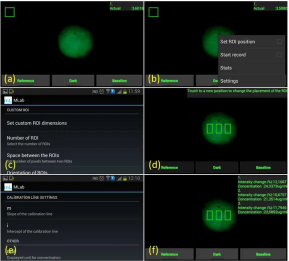
continuously at the background. First, region of interests (ROI) on the sensor surface are defined by tapping menu button and entering ROI parameters in the settings menu. To estimate analyte concentrations from intensity changes, predetermined calibration line parameters are set in slope, intercept and unit fields. Time averaging feature can be activated by entering the number of consecutive frames to be averaged. “Reference”, “Dark” and “Baseline” buttons are used to take and store reference, dark and baseline intensity values, respectively, as described in subsection 3.2.3. Averaged intensity changes and estimated analyte concentrations for each ROI segment are displayed separately on the right side of the screen when the “Start recording” box is checked. Unchecking the “Start recording” item stops recording and saves measurement data in a text file. Screen captures from application software are presented in Fig. 3.2.
Figure 3.1: Surface plasmon resonance imaging platform integrated with a smartphone. (a) Schematic illustration and (b) photograph of the imaging apparatus. (c) Custom developed smartphone application for real-time and on-site
Figure 3.2: Smartphone application software. (a) When the app is started, zoomed in view of the imaging spot is displayed at the background overlaid by “Button menu” at the bottom, and “Report table” at the top right corner. (b) “Control menu” pops up at the bottom right corner when the menu button of the smartphone is tapped. (c) Region of interest (ROI) parameters are defined in the “Settings menu”. (d) ROI frames are overlaid on the imaging spot. (e) Other input values like calibration line parameters and number of averaging frames are entered in the “Settings menu”. (f) Following the measurement of reference, dark and baseline intensities by using the buttons in the “Buttons menu”, actual measurement is initiated by checking the “Start record” item in the “Control menu”, and averaged intensity change and estimated analyte concentrations for each ROI are updated separately in the “Report table”. Measurement data is automatically saved in a text file when the recording is stopped by unchecking the “Start record” item.
3.2.2 Design and fabrication of SPRi sensor chips
Optical storage discs can be exploited as grating coupled surface plasmon resonance sensors by metal coating, thanks to the periodic corrugations (Fig. 3.3) [39], [57].
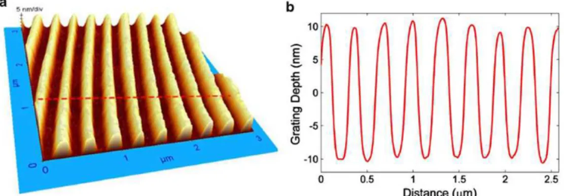
Figure 3.3: (a) AFM micrograph of Blu-ray disc surface and (b) line profile.
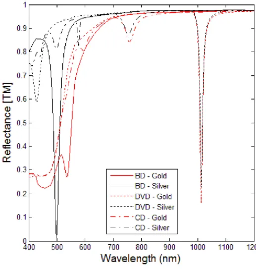
Depending on the disc type and refractive index of the surrounding medium, surface plasmons can be excited at wavelengths ranging from ultraviolet to near infrared spectral regions. SPR substrates produced from Blu-ray discs (BD) (grating period Λ=320 nm, grating depth d=20 nm) exhibit plasmon resonances within the visible spectrum when illuminated at normal incidence in aqueous medium, as indicated by the reflectance spectra calculations (Fig. 3.4).
Figure 3.4: Calculated reflectance spectra of various types of metallized optical discs under normal incidence of illumination in water medium. Grating periods of Blu-ray Disc (BD), Digital Versatile Disc (DVD) and Compact Disc (CD) are 320 nm, 740 nm and 1.6 µm, respectively.
Numerical calculations are performed using a commercial software which employs modified integral method (MIM) [40]. PCGrate allows calculation of diffraction efficiencies of multilayered 1-D gratings. Calculation mode should be switched from normal to resonance mode for SPR coupler simulations. Polarization of the incident beam is set as non-polarized in order to examine the reflectance spectra for both transverse electric (TE) and transverse magnetic (TM) polarized illuminations. Surface profile of the grating on BD is defined as
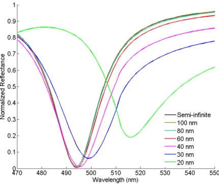
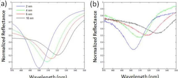
sine-According to the simulation results, silver coated BD exhibits sharp plasmon resonance around 500 nm wavelength, whereas gold coated BD does not display surface plasmon resonant behavior at normal incidence of excitation due to its intrinsic absorption characteristics at this portion of the spectrum. However, gold has superior properties over silver in terms of chemical stability and adequacy for further surface functionalization chemistry for biosensing applications. In order to overcome this dichotomy, we came up with a hybrid solution in which thick (>80 nm) silver coating at the bottom acts as a plasmon excitation layer and thin (<10 nm) gold film on top functions as a surface for the subsequent surface modification, as well as extending the shelf life of the sensor chip. The thicknesses of Ag and Au layers are optimized using numerical simulations. Silver layer thickness above 80 nm is found to yield almost same SPR reflectance spectra with semi-infinite silver layer configuration as shown in Fig. 3.5. As the thickness of the top gold layer is increased, on the other hand, plasmon resonance curve degrades and loses its sharpness as shown in Fig. 3.6. Thus, gold coating thickness is kept as 2 nm in order to satisfy both sensitivity and surface chemistry requirements. Apart from the previous studies which use the Ag/Au bimetallic structure to increase sensitivity [53]–[56], we used this configuration to obtain a response below 520 nm which is not possible with the commonly used single gold layered couplers.
Figure 3.5: Calculated SPR reflectance spectra of Ag coated BD chip under normal incidence of illumination in water medium with respect to decreasing silver thickness. As the thickness of silver layer reduces below 80 nm, SPR curve loses its sharpness due to the interaction of surface plasmon wave with the underlying substrate layer.