GRAPHENE-BASED ELECTRICALLY
TUNABLE TERAHERTZ OPTOELECTRONICS
A DISSERTATION SUBMITTED TO
THE GRADUATE SCHOOL OF ENGINEERING AND SCIENCE OF BILKENT UNIVERSITY
IN PARTIAL FULFILMENT OF THE REQUIREMENTS FOR THE DEGREE OF DOCTOR OF PHILOSOPHY IN PHYSICS
By
Nurbek Kakenov
September 2016
ii
GRAPHENE-BASED ELECTRICALLY TUNABLE TERAHERTZ OPTOELECTRONICS
By Nurbek Kakenov September 2016
We certify that we have read this thesis and that in our opinion it is fully adequate, in scope and in quality, as a dissertation for the degree of Doctor of Philosophy.
___________________________________________ Coşkun Kocabaş (Advisor)
___________________________________________ Mehmet Özgür Oktel ___________________________________________ Ömer Dağ ___________________________________________ Hakan Altan ___________________________________________ Alphan Sennaroğlu
Approved for the Graduate School of Engineering and Science:
___________________________________________ Ezhan Karaşan
iii
Copyright Information
Copyright Disclaimer: Content of Figure 2.10(a) in chapter 2 is reprinted (adapted)
with permission from (L Ren, Q Zhang, J Yao, Z Sun, R Kaneko, Z Yan, S Nanot, Z Jin, I Kawayama, M Tonouchi, J M. Tour, and J Kono “Terahertz and Infrared
Spectroscopy of Gated Large-Area Graphene” Nano Letters 2012 12 (7),
3711-3715). Copyright 2012 American Chemical Society (ACS).
Copyright Disclaimer: Content of Figure 2.10(b) in chapter 2 is adapted by
permission from Macmillan Publishers Ltd: [NATURE COMMUNICATIONS] (S-R, Berardi Y, R Kelly, Michelle M. F, Tian T, Kristof H, Wan Sik J, Debdeep L, Lei X, H Grace, “Broadband graphene terahertz modulators enabled by intraband
transitions” Nat Commun, 2012. 3: p. 780-786), copyright (2012).
Copyright Disclaimer: Content of the Figure 2.10(c) in chapter 2 is reprinted
(adapted) with permission (B S-Rodriguez, R Yan, S Rafique, M Zhu, W Li, X Liang, D Gundlach, V Protasenko, M M. Kelly, D Jena, L Liu, and H G Xing “Extraordinary
Control of Terahertz Beam Reflectance in Graphene Electro-absorption Modulators” Nano Letters 2012 12(9), 4518-4522). Copyright 2012 American
Chemical Society (ACS).
Copyright Disclaimer: Content of Figure 2.10(d) in chapter 2 is adapted by
permission from Macmillan Publishers Ltd: [NATURE MATERIALS] (Vicarelli, L.,Vitiello, M. S. Coquillat, D. Lombardo, A. Ferrari, A. C.Knap, W. Polini, M. Pellegrini, V. Tredicucci, A.., Graphene field-effect transistors as room-temperature
terahertz detectors. Nat Mater, 2012. 11(10): p. 865-871.), copyright (2012).
Copyright Disclaimer: Contents of chapter 5 are published in Journal of Optical
Society of America B-Optical Physics as “Broadband terahertz modulators using
self-gated graphene capacitors” N Kakenov, O Balci, E O Polat, H Altan, C
Kocabas, Journal of the Optical Society of America B-Optical Physics, 2015 32(9): p.1861-1866, and reproduced in chapter 5 with permission of The Optical Society (OSA). Copyright 2015 OSA. Systematic or multiple reproduction or distribution to multiple locations via electronic or other means is prohibited and subject to penalties under law.
iv
Copyright Disclaimer: Contents of chapter 6 are published in ACS Photonics as
“Observation of Gate-Tunable coherent Perfect Absorption of Terahertz Radiation
in Graphene” N Kakenov, O Balci T Takan, V A Ozkan, H Altan, C Kocabas, ACS
Photonic, 2016. 3(9): p. 1531-1535, and reproduced in chapter 6 with permission of
American Chemical Society (ACS). Copyright 2016 ACS. Systematic or multiple reproduction or distribution to multiple locations via electronic or other means is prohibited and subject to penalties under law.
Copyright Disclaimer: Contents of this chapter are published in Optics Letters as
“Graphene-enabled electrically controlled terahertz spatial light modulators” N
Kakenov, T Takan, V A Ozkan, O Balci, E O Polat, H Altan, C Kocabas, Optics Letters 40(9), 2015, pp. 1984-1987, and reproduced in chapter 7 with permission of
The Optical Society (OSA). Copyright 2015 OSA. Systematic or multiple reproduction or distribution to multiple locations via electronic or other means is prohibited and subject to penalties under law.
v
ABSTRACT
GRAPHENE-BASED ELECTRICALLY TUNABLE
TERAHERTZ OPTOELECTRONICS
Nurbek Kakenov Ph.D. in Physics Advisor: Coşkun Kocabaş
September 2016
Advances in terahertz (THz) research and technology, has bridged the gap between radio-frequency electronics and optics. More efficient control of THz waves would highly benefit noninvasive, high-resolution imaging and ultra-fast wireless communications. However, lack of active materials in THz, hinders the realization of these technologies. Graphene, 2d-crystal of carbon atoms, is a promising candidate for reconfigurable THz optoelectronics due to its unique electronic band structure which yields gate-tunable optical response. Here, we studied gate-tunable optical properties of graphene in THz frequencies. Using time-domain and continuous wave THz spectroscopy techniques, tunable Drude response of graphene is investigated at very high doping levels with Fermi energies up to 1 eV. Our results show that, transport scattering time decreases significantly with doping. Unlike conventional semiconductors, we observed nearly perfect electron-hole symmetry even at very high doping levels. In the second part, we implemented using these unique tunable properties for novel THz optoelectronic devices such as THz intensity modulators and THz spatial light modulators. These devices are based on various designs of mutually gated capacitive structures consisting of ionic liquid electrolyte sandwiched between graphene and metallic electrodes. Low insertion losses (<2 dB), high modulation depth (>50 %) over a broad spectrum (0.1-2 THz), and the simplicity of the device structure are the key attributes of graphene
vi
based THz devices. Furthermore, with the optimized device architectures, gate tunable coherent perfect absorption is observed in THz which yields modulation depth of nearly 100 %. The approaches developed in this work surpass the challenges of generating high carrier densities on graphene, and introduce low-loss devices with practical fabrication methods which we believe can lead to more responsive and sophisticated optoelectronic devices.
Keywords: graphene, Drude conductivity, modulator, THz-Spatial light modulators,
vii
ÖZET
GRAFEN-TABANLI ELEKTRİK AYARLI
TERAHERTZ OPTOELEKTRONİĞİ
Nurbek Kakenov Fizik, Doktora
Tez Danışmanı: Coşkun Kocabaş Eylül 2016
Radyo-frekans elektroniği ile optiğin arasında boşluk olan terahertz (THz) bandı son yıllardaki gelişmelerle birlikte dolmaya başladı. Daha verimli terahertz dalga kontrolü optoelektronik uygulamaları olumlu yönde etkileyecek en önemli parametrelerden biri. Var olan yöntemlerin daha aktif, uygulanabilir, az masraflı, ve verimli hale gelmesi için detaylı çalışmaların sürdürülmesi gerekli. Grafen bu alandaki gelişmeler için en önemli materyal adayı konumunda. Eşsiz elektronik ve optik özelliklere sahip olan grafen terahertz alanında aktif olarak kullanabilme potansiyelini taşımaktadır. Bu çalışmada grafen tabanlı modülatör, resonans kavite, ve THz mekansal ışık modülatorleri geliştirildi. Geliştirilen yeni yöntemler daha verimli yük yoğunluğu yaratmakta, sistemdeki kayıplar (<2 dB) azaltmakta ve aygıt yapılarını kolaylaştırmakta. Grafen elektrodlarının ortak iyoniksel kapılamalarını kullanarak 0.1 ve 2 THz frekans aralığında %50 modülasyon değişikliğini elde etmiş olduk. Yansınma bazlı kavite geliştirerek terahertz dalga absorpsiyonunu 2.8 THz frekansında yaklaşık %100 oranında arttırabildik. Son olarak geniş bantta çalışabilen THz mekansal ışık modülatör aygıtlarını grafen süperkapasitörlerini kullanarak elde ettik. Grafenin aktif olarak terahertz bandında kullanılması, daha verimli ve sofistike THz optoelektronik aygitlarin gelişmesini sağlayabilir.
Anahtar sözcükler: grafen, Drüd iletkenliği, modulator, THz mekansal ışık
viii
Acknowledgement
I express my most sincere gratitude and appreciation to my advisor Prof. Coşkun Kocabaş. Not only his guidance and support have always leaded me, but also motivated me throughout the time of my research and study. Without his guidance and supportive attitude, this dissertation would not have been possible.
I, as well, present my gratitude to Prof. Mehmet Özgür Oktel, Prof. Ömer Dağ, Prof. Hakan Altan, and Prof. Alphan Sennaroğlu for their judgments and helpful critics as the thesis committee.
Especially, I am thankful to Prof. Hakan Altan and his students Taylan Takan and Ali Vedat Özkan for collaborations. Without their help none of the terahertz measurements would have been possible.
I would like to thank Kocabaş Research Group, both present and former members for providing me wonderful atmosphere during the course of the years. Namely, I thank Dr. Evgenia Kovalska, Dr. Ömer Salihoğlu, Dr. Emre Polat, Dr. Murat Yıldırım, Dr. Eda Goldenberg, Shahnaz Aas, Pınar Köç, Burkay Uzlu, Doolos Aibek Uulu, Uğur Demirkol, Zeinab Eftekhari.
Above all, I am grateful to Dr. Sinan Balcı and Dr. Osman Balcı for their support and guidance throughout the years that I spent at Bilkent University.
I would like to thank my friends Salamat Burzhuev, Kanat Jakshybekov, Aktan Aidarov, Erçağ Pinçe, Melike Gümüş, Özge Akay, Simge Ateş, Abdullah Muti, Seval Sarıtaş, Ertuğrul Karademir, Mehmet Günay, and Özlem Yavaş.
I am also thankful to the faculty and staff of Advanced Research Laboratory and Department of Physics for providing me delightful atmosphere throughout my study.
ix
I would like to thank TÜBİTAK-BİDEB for the fellowship program 2215-PhD Fellowship for International Students and projects (114F052, 113F278, 112T686, 109T259) for funding supports.
I dedicate this dissertation to my family, whom I owe my profound gratitude. I am thankful to my father Meder Asanbekov, my mother Sveta Konurbaeva, my brothers Nurlan Asanbekov and Nursultan Meder Uulu, my aunts Dr. Roza Konurbaeva, Zakultai Konurbaeva, Zarema Asanbekova, Nazgul Asanbekova, my uncles Aibek Asanbekov, Talant Konurbaev, my grandmother Lima Asanbekova, my grandfather Esenaman Konurbaev and all other members of my family for their love, care, and patience.
x
xi
Contents
1 Introduction 1
2 Terahertz Optoelectronics 8
2.1 Introduction... 9
2.2 Terahertz optoelectronic devices ... 9
2.3 Continuous wave terahertz components ... 11
2.4 Time domain terahertz spectroscopy ... 15
2.5 Graphene-enabled terahertz optoelectronic devices ... 23
2.6 Conclusion ... 25
3 Optical Properties of Graphene 27 3.1 Electronic band structure of graphene ... 28
3.2 Electrical gating of graphene ... 29
3.3 Optical properties of graphene... 31
3.4 Synthesis of graphene ... 40
3.5 Transfer process of graphene ... 44
4 Drude Response of Highly Doped Graphene 48 4.1 Introduction... 49
4.2 Fourier transform spectroscopy measurement of graphene ... 50
4.3 Extracting Fermi energy of graphene ... 56
4.4 Measuring Drude-like response of graphene ... 58
xii
5 Controlling Terahertz Waves with Graphene Supercapacitors 64
5.1 Introduction... 64
5.2 Optical and electrical characterizations of graphene devices ... 72
5.3 Broadband THz beam modulation using graphene supercapacitors... 73
5.4 Graphene based large-area terahertz modulator ... 75
5.5 Conclusions ... 78
6 Coherent Perfect Absorption of THz Radiation in Graphene 80 6.1 Introduction... 80
6.2 Graphene-based terahertz cavity... 83
6.3 Observation of coherent perfect absorption in graphene ... 86
6.4 Sub-terahertz continuous wave reflectance ... 93
6.5 Transport scattering time at highly doped graphene ... 95
6.6 Flexible active terahertz surface ... 96
6.7 Conclusion ... 98
7 Terahertz Spatial Light Modulators 99 7.1 Introduction... 99
7.2 Fabrication of graphene-enable multipixel THz device ... 100
7.3 Controlling THz transmittance with graphene-enabled THz-SLM ... 102
7.4 Modelling THz transmittance of the device ... 107
7.5 Conclusions ... 108
8 Summary 109
xiii
List of Figures
Figure 1.1 Absorption spectrum of single layer graphene from visible to microwave wavelengths. The images shows the active THz devices studied in this thesis. ... 5 Figure 2.1 Electromagnetic spectrum. THz region is located between microwaves
and infrared frequencies. ... 10 Figure 2.2 Schematic drawing of Golay Cell thermal detector. ... 13 Figure 2.3 CW terahertz reflectance measurement system. To generate CW (0.24
to 0.38 THz) a YIG oscillator integrated with VDI multiplier is used. 14 Figure 2.4 Terahertz time-domain spectroscopy (THz-TDS) schematics. Optical
beam is split into two pulses. First pulse (pump) impinges on THz emitter (nonlinear crystal, or PC diode) to generate subpicosecond THz pulse. The second pulse (probe) undergoes time delay and impinges on THz detector. The probe pulse is used to gate the THz detector (Schottky diode, PC antenna). ... 16 Figure 2.5 THz pulse emitter based on photoconductive antenna. ... 17 Figure 2.6 THz receiver. (a) Probe pulse is impinges on dipole structure of THz
receiver causing extra free carriers. When THz pulse hit on dipole structure, it causes detectable photocurrent flow. (b) Side view of THz
xiv
detector antenna. By changing the time delay, whole electric field profile of THz pulse is mapped out. ... 19 Figure 2.7 Schematic view of terahertz time domain spectroscopy measuring
system. ... 20 Figure 2.8 THz pulse emission in a nonlinear crystal. ... 21 Figure 2.9 Electro-optic system to detect terahertz pulses based on nonlinear
crystals. ... 23 Figure 2.10 (a) Transistor type graphene device ©2012 ACS [37]. (b) Graphene
based THz intensity modulator ©2012 NPG [27]. (c) Reflection type THz intensity modulator ©2012 ACS [48]. (d) Graphene-based field effect THz detector ©2012 NPG [26]. All figures were reprinted with
permission from corresponding publication groups. ... 25
Figure 3.1 Crystal structure of graphene (a) Hexagonal crystal structure of graphene (left). Units cell indicated as dashed area with corresponding unit vectors (a1, a2). There two atoms in unit cell. (b) reciprocal lattice
and vectors. First Brillioun zone of hexagonal structure with unit vectors (b1, b2). Dirac points are each hexagon corners. ... 28
Figure 3.2 Gating methods of graphene (a-c) General gating methods used to control the electronic properties of graphene. (d) Schematic representation of the voltage drop across the gate terminals of dielectric and electrolyte devices. Voltage linearly drops between the graphene and gating electrodes for solid dielectric based devices, blue line. However, voltage is constant across the electrodes and drops rapidly at the interfaces of the electrodes, red line. Electrical double layers created induce high electric fields at the interfaces. ... 31
xv
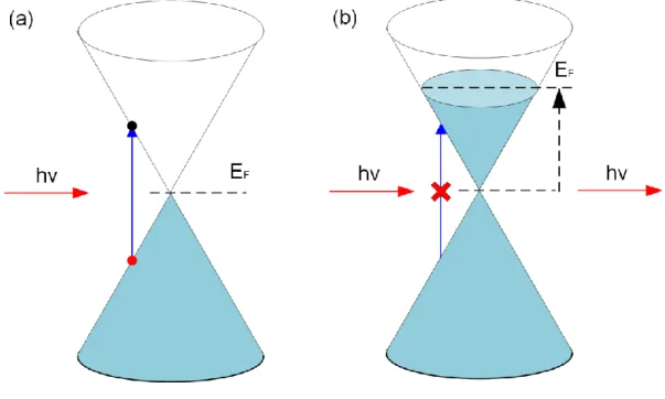
Figure 3.3 Optical response of graphene from visible to microwave region of electromagnetic spectrum. At visible-near infrared, interband transitions dominate absorbing 2.3 % of incident energy. At low energies, THz-microwave, intraband transitions dominate. The maximum of 50 % energy can be absorbed by single layer graphene. . 32 Figure 3.4 Pauli blocking. (a) Interband electronic transition occurs when the
electron in valence band is excited to conduction band by photon absorption. The photon is absorbed when its energy exceed 2EF. (b)
This absorption cannot take place if the Fermi energy of graphene is higher than photon’s energy. ... 34 Figure 3.5 The dependence of real and imaginary values of complex conductivity
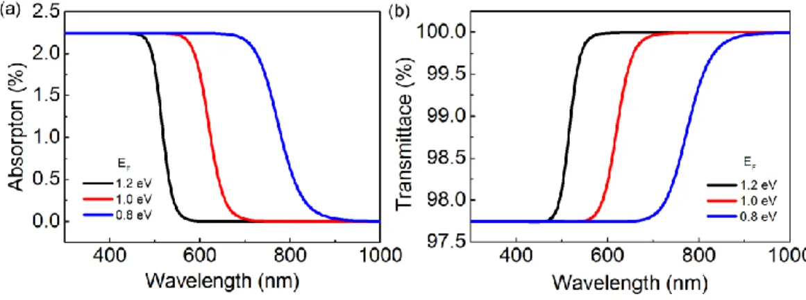
of graphene on temperature. ... 36 Figure 3.6 (a) Absorption of a single layer graphene as a function of Fermi energy.
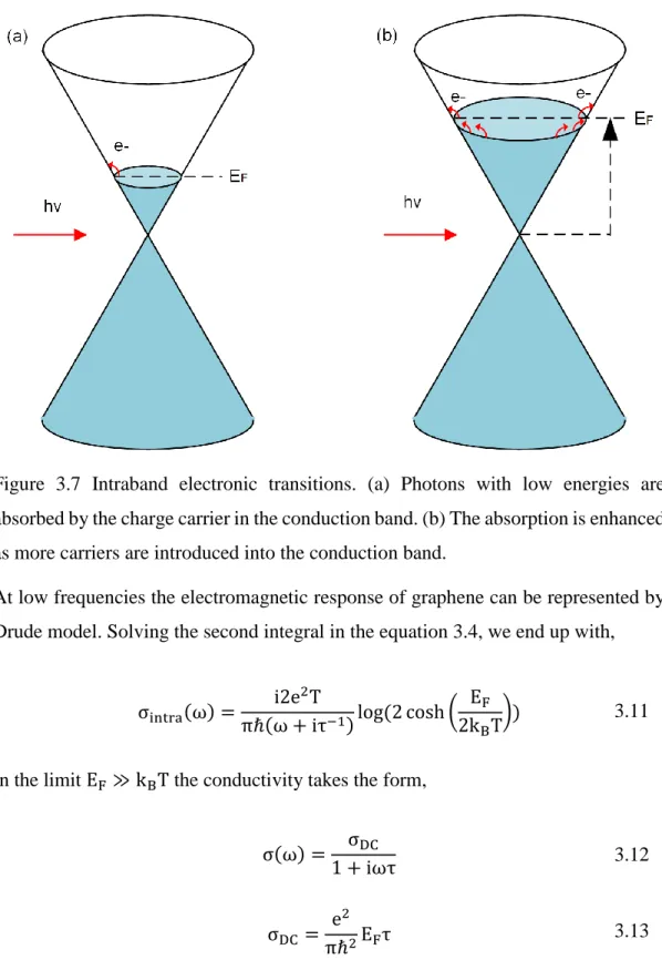
2.3 % of incident wave is absorbed when the photon energy is the twice the Fermi energy. As the Fermi energy shifts to higher levels, the more energetic photons are blocked. (b) Transmittance spectrum of monolayer graphene at various values of Fermi level. ... 37 Figure 3.7 Intraband electronic transitions. (a) Photons with low energies are
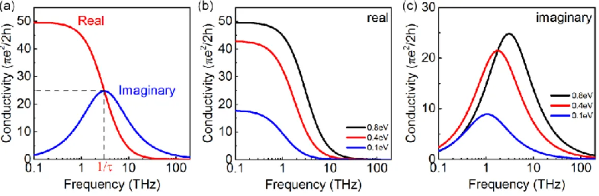
absorbed by the charge carrier in the conduction band. (b) The absorption is enhanced as more carriers are introduced into the conduction band. ... 38 Figure 3.8 Drude conductivity of monolayer graphene. (a) Real and imaginary
parts of Drude conductivity. The frequency value at the intersection of two curves corresponds to carrier scattering rate. (b) Real conductivity at different Fermi energy values. (c) Imaginary conductivity at different Fermi energy values. ... 39
xvi
Figure 3.9 (a) Copper foils are cut and placed on quartz holder. The size is limited by the holder 7x30 cm2. (b) Quartz chamber embedded in furnace,
where the synthesis occurs. ... 41 Figure 3.10 CVD system. (a) Furnace with quartz chamber, which can go up to
1070 degrees. The pump is used to vacuum the chamber. (b) Before the growth the chamber is vacuumed down to 3-6 mTorr. ... 42 Figure 3.11 (a) The gases used during the growth are methane (CH4) as carbon
source and hydrogen (H2) to anneal the copper surfaces. ... 43
Figure 3.12 Transfer printing process. (a) Shipley 1813 PR is dropped on CVD grown graphene, and baked overnight at 65 degrees. (b) Copper is etched in iron chloride solution. The baked PR is used as a holder of graphene. (c) When all copper is etched, PR holding graphene is placed on a substrate (Polyethylene). (d) To transfer graphene on to substrate the sample is heated. (e) Then PR is washed with acetone/IPA. (f) The transferred single layer graphene on polyethylene membrane. ... 45 Figure 3.13 Transferring graphene via lamination. (a) Laminating machine. CVD
grown graphene samples are arranged on paper covered by PVC from both sided. (b) Laminated graphene. Graphene is sandwiched between Cu film (top) and PVC polymer (bottom). The tapes are used to cover the contacts. (c) Copper is removed via wet etching. ... 46 Figure 3.14 Laminated graphene. (a) Graphene sample after copper has been
removed. (b) The laminated graphene sample with contacts. (c) The conductance of transferred graphene. ... 47 Figure 4.1 Schematic representation of device design. The device consists of gold
layer, electrolyte medium and graphene on membrane. The gold on substrate with circular opening allows beam to pass through graphene
xvii
without any interaction. As an electrolyte we used ionic liquid to efficiently gate graphene. The graphene is CVD grown and transferred on THz transparent polyethylene membrane. ... 52 Figure 4.2 FTIR measurement setup. FTIR has both wide range source (VIS, NIR,
FIR) and detectors. ... 53 Figure 4.3 (a) Capacitance, (b) resistance of the graphene device as a function of
bias voltage. The charge neutrality point occurred at 1.1 V. ... 55 Figure 4.4 Visible and NIR spectrum of graphene device. Differential
transmittance of for (a) hole (b) electron doping at different Fermi energies. (c) and (d) represents the mid infrared differential transmittance for hole and electron doping of graphene device at various Fermi energies. ... 56 Figure 4.5 (a) Photograph of fabricated device. Graphene on polyethylene
membrane on top of 60 nm gold on PVC substrate with 8 mm opening. (b) The Fermi level shift of graphene from -4 V to 4 V. ... 57 Figure 4.6 Graphene’s response at THz frequencies. Transmittance of single layer
graphene as a function of frequency at various gating voltages (a) hole (b) electron regime. The extracted ac conductivity of single layer graphene from transmittance for (c) and (d) hole and electron doping. The color bar represents the gating voltage levels. ... 59 Figure 4.7 Drude parameters of highly doped graphene. (a) Sheet resistance of
graphene changes from doped (500 Ω/sq) to undoped (4 kΩ/sq). (b) DC conductivity or (Drude weight) changes linearly for both electrons and holes. The transport scattering time as a function of Fermi energy of graphene at (c) hole (d) electron regimes. The hole and electron carries exhibit symmetric behavior. The mean free path of carriers are highly dependent on Fermi energy. ... 62
xviii
Figure 5.1 (a) Schematic representation of the graphene supercapacitor used as a broadband THz modulator. The supercapacitor consists of ionic liquid electrolyte sandwiched between two large-area graphene electrodes. The charge density on graphene electrodes is modulated efficiently by an external voltage applied between the graphene electrodes. (b) Schematic band structure of electrostatically doped graphene electrodes. The arrows represent the interband and intraband electronic transitions. (c) Equivalent transmission line model of the graphene layer. (d) Calculated optical absorption of single-layer graphene plotted against the frequency for different doping levels. (e) Change of reflection, transmission, and absorption of graphene as a function of sheet resistance. The shaded area indicates the experimentally accessible sheet resistance for CVD graphene. ©2015 OSA ... 67 Figure 5.2 (a) Modulation of the optical transmittance of the graphene
supercapacitor in the visible spectra. (b) Variation of the capacitance of the devices and extracted Fermi energy of the graphene electrodes as a function bias voltage. (c) Variation of the resistance of the graphene electrodes with the bias voltage. (d) Calculated charge density is plotted against the bias voltage. The solid line is calculated from the capacitance, whereas the scattered points are calculated from the measured Fermi energy. ©2015 OSA ... 71 Figure 5.3 (a) Time-varying electric field of the THz pulse at various voltage bias
between 0 and −2.5 V. The reference THz signal is measured without the graphene supercapacitor. (b) Modulation of the maximum electric field as a function of bias voltage. (c) Spectrum of the transmitted THz pulse obtained after Fourier transform of the transmitted signal and
xix
normalization with the reference signal. (d) Modulation of signal at 0.6 THz. ©2015 OSA ... 75 Figure 5.4 (a) Picture of the large-area (7×7 cm) THz modulator. (b) Variation of
the capacitance of the modulator as a function of bias voltage. (c) Capacitance of the modulator at different sizes. (d) Extracted cutoff frequency as a function of device size. (e) Time-varying electric field of the THz pulse at various voltage bias between 0 and −3 V. (f) Spectrum of the transmitted THz signal obtained after Fourier transformation of the recorded signal and normalization with the signal at a bias voltage of 0 V. ©2015 OSA ... 77 Figure 5.5 (a) Insertion loss of the total device and the graphene electrodes plotted
against the frequency. (b) Comparative graph showing the modulation depth and intrinsic insertion loss of graphene modulators. ©2015 OSA ... 78 Figure 6.1 Schematic drawing of free standing graphene and active THz surface
and their transmission line models. In the case of free standing graphene, the maximum absorbance is achieved when the surface impedance of graphene (ZG) matches the half of the free space
impedance (Z0). For the device, metallic reflecting surface is modeled
as a short circuit at a quarter wave distance from the graphene. The quarter wave transmission line converts the short circuit in to an open circuit. In this case, the maximum absorbance is achieved when the surface impedance of graphene is Z0. Here the surface impedance of
graphene refers impedance due to optical conductivity.©2016 ACS ... 82 Figure 6.2 Terahertz transmittance spectrum of porous polyethylene (PE) and PE
xx
Figure 6.3 Active THz surfaces (a) Schematic representation of electrically tunable THz cavity used for the coherent perfect absorption in graphene. The THz cavity is formed by a porous membrane sandwiched between graphene and gold electrodes. The thickness of the membrane is 20 µm. The ionic liquid electrolyte is soaked into the membrane. (b) Cross-sectional view of the cavity showing the formation of electrical double layers on the graphene and gold electrodes. ©2016 ACS ... 86 Figure 6.4 Coherent perfect absorption of THz radiation (a) Photograph of the
fabricated THz cavity. The monolayer graphene is transferred on PE membrane and placed on a gold coated substrate. The 20-µm-thick membrane defines the cavity length, holds the electrolyte and forms the mechanical support graphene. (b) Experimental setup used for the THz measurements. (c) The Reflectivity spectrum from the device at different bias voltages. (d) The variation of the resonance reflectance with gate voltage. The charge neutrality point is at -1 V. ©2016 ACS 88 Figure 6.5 Electrical and optical characterization of the device (a) Schematic
representation of the band structure of graphene and possible electronic transitions. (b) Gate-tunable near-IR optical reflection from the graphene surface at different bias voltages. The number on the curves shows the bias voltage. (c) Fermi energy extracted from the reflection spectrum. (d) Variation of the resistance and capacitance of the devices with the bias voltage. At charge neutrality point, resistance reaches a maxima of 4.5 kΩ and the capacitance goes to a minima of 0.8 µF/cm2. ©2016 ACS ... 90
Figure 6.6 (a) Voltage-controlled IR reflectivity of the active THz surface and (b) the extracted Fermi energies at low bias voltages. ©2016 ACS ... 91
xxi
Figure 6.7 Tunable reflectivity from various THz cavities: Reflectance spectrum of THz cavities with 40 and 60 µm membrane thickness. ©2016 ACS ... 92 Figure 6.8 (a, b) The reflectivity spectra of individual resonances at 3.6 and 8.5
THz at different gate voltages. (c) Variation of the resonance frequency and the FWHM of the resonances. We do not observe a significant shift in the resonance frequency however, the FWHM increases slightly with the bias voltage. ©2016 ACS ... 93 Figure 6.9 (a) Schematic drawing of the experimental setup used for reflectivity
measurements at 0.368 THz. A Virginia Diode, Inc. Schottky diode (VDI), based, multiplied mm-wave/THz emitter is used as a tunable frequency signal source (WR9.0AMC+WR2.8X3). Driven by a voltage-controlled frequency-tunable YIG oscillator, the system can provide a minimum average output power of about 1 mW. The output of the source is amplitude modulated via function generator in order to detect the radiation with a Golay Cell (Tydex TC-1T). (b) The normalized reflectivity plotted as a function of bias voltage. We obtained a modulation of 98 % at 0.368 THz. ©2016 ACS ... 94 Figure 6.10 Drude response of graphene at high doping level (a) Frequency
dependence of the resonance absorbance at different Fermi energies. The absorbance is normalized by maximum absorbance at 2.8 THz. (b) The variation of the transport scattering time with the Fermi energy. ©2016 ACS ... 95 Figure 6.11 Flexible active THz surfaces (a) Photograph of the large area graphene
on PE membrane and gold coated PVC substrate. (b) The fabricated device rolled around a glass cylindrical with diameter of 2.7 cm. (c)
xxii
THz reflectivity spectrum from the curved surface at different bias voltages. ©2016 ACS ... 97 Figure 7.1 (a) Schematic drawing of the THz spatial light modulator consisting of
a 5×5 array of graphene supercapacitors. (b) Photograph of the fabricated device mounted on a printed circuit board. The size of an individual pixel is 8 mm×8 mm. ©2015 OSA ... 102 Figure 7.2 (a)–(d) THz transmission images of the SLM with various voltage
configurations recorded at a frequency of 0.37 THz. (e) Transmittance of the device at 0.37 THz as a function of bias voltage. (f) Histogram of the transmittance at bias voltage of 0 and 2 V. (g) Variation of the capacitance (left axis) of the device and estimated charge density (right axis) as a function of bias voltage. Two distinct minima are associated with the Dirac points of the top and bottom graphene electrodes. (h) Voltage-dependent transmittance at different frequencies. ©2015 OSA ... 104 Figure 7.3 (a) THz pulse recorded at bias voltages of 0, 1, and 2 V. (b) Modulation
plotted against frequency. The scattered points show the data recorded with our mm-wave/THz system. ©2015 OSA ... 105 Figure 7.4 (a) Schematic illustration of cross section of the device and (b) charge
distribution on the graphene electrodes biased at different voltages. (c) Line profile of the THz transmission along the grounded row. (d) Variation of the modulation and cross talk of single pixel with bias voltage. ©2015 OSA ... 106 Figure 7.5 (a) Calculated THz transmittance of single-layer graphene. (b)
1
Chapter 1
Introduction
Since its discovery, graphene research has taken considerable amount of progress in synthesis and device implementations. Both theoretical and experimental studies have manifested extraordinary electrical, mechanical, and optical properties of graphene. Its distinct nature lie in hexagonal lattice structure where carbon atoms undergo sp2 hybridizations to create in-plane sigma and out of plane 𝜋 bondings. In-plane covalent bondings make graphene mechanically strong, while weak out of plane orbitals account for the unique electronic and optical properties. The linear relationship between energy and momentum give rise to massless Dirac fermions within Dirac approximation. Unlike semiconductor carriers with parabolic dispersion relation, electrons and holes in graphene mimic zero mass particles which exhibit very large carrier mobilities. High carrier mobility (200,000 cm2/Vs) [1], together
with electrically tunable optical response of graphene, offers new opportunities in optoelectronic devices especially at terahertz frequencies. Although graphene is only one-atom-thick, it can be seen by the naked eye. This phenomenon arises from nearly frequency independent 2.3 % absorbance at optical wavelengths [2-4]. These interesting optical properties can be tuned by controlling charge density on graphene which could yield new optical devices operating in a very broad spectrum.
2
Especially graphene could be a unique active material for terahertz frequencies. Electromagnetic waves with terahertz frequencies can be used for very high-speed communication [5] or nonionizing, high resolution imaging systems [6, 7]. These systems require active optoelectronic components such as emitters, detectors, modulators, switches, and other devices. With recent developments in THz research, THz sources and detectors have become more advanced however, active THz modulators and switches still need further improvements. Due to the lack of active THz materials it has been a challenge to control terahertz waves [8]. The submillimeter spatial resolution, and nonionizing nature are the essential properties of terahertz waves that can enable improvements in medicine, pharmaceuticals, security, communications, etc. These emerging technologies would greatly benefit from more efficient control of THz waves [9, 10]. Due to its unique electronic band structure which yields gate-tunable optical response, graphene is a promising material for reconfigurable THz optoelectronics.
In Chapter 2, we explain the electronic and optical properties of graphene followed by synthesis and transferring methods. Many studies [11-13] demonstrated the electronic band structure of graphene approximating by tight-binding model. The optical conductivity can derived from Kubo formalism [4, 14]. Under Dirac cone approximation, graphene exhibits linear dispersion relation. Optical responses of graphene arises from its unique band structure. Graphene has nearly frequency independent absorption at visible and near-infrared region of the spectrum. This absorption arises from universal conductance of e2/4ħ, Figure 1.1. For longer
wavelength, THz and microwave region, intraband absorption is successfully explained with frequency dependent Drude model. By combining interband and intraband transitions, graphene provides a unique platform to control light-matter interaction in a very broad spectrum ranging from visible to microwave. This broad band activity enables us to design new electrically tunable optoelectronic devices.
3
After an enormous amount of research, methods to synthesize graphene have been improved. In this thesis, chemical vapor deposition (CVD) method is utilized to grow large graphene samples that enable us to realize active THz devices. By using CVD method, it is possible to produce large area graphene sheets limited only by the chamber size. This technique is more practical compared with mechanical exfoliation and epitaxial growth, also it is industrially promising. CVD grown graphene can be transferred on both solid and flexible substrates. We have optimized our technique to transfer graphene on terahertz transparent substrates such as quartz, polyethylene, PVC, and others. At the end of Chapter 2, the details of these methods were summarized.
In Chapter 3, we briefly discuss terahertz optoelectronics and graphene based THz devices reported in the literature. Advances in science and technology have greatly contributed in closing the THz gap by developing more efficient emitters, detectors modulators, and other devices. More efficient control of THz waves would highly benefit noninvasive, high-resolution imaging and ultra-fast wireless communications. There are two main methods for THz characterization, the time-domain and continuous wave. Conventional time-domain spectroscopic systems use photoconductive (PC) antennas and nonlinear crystals for both emitting and detecting terahertz signals. Terahertz time-domain spectroscopy (THz-TDS) offers broadband spectral range measurements and extra freedom in measuring parameters such as phase information. However, THz-TDS systems utilize femtosecond lasers which brings complexity to these measuring systems. Unlike THz-TDS, continuous wave systems are more practical and compact. It can use YIG oscillators, quantum cascade lasers, Photomixing devices, etc.. To detect CW terahertz radiation thermal detectors can be used such as bolometers, Golay cell, and pyroelectric devices. Still lack of active materials hinders the realization of more efficient THz optoelectronic devices. Graphene with its unique electrical and optical properties is a promising candidate to facilitate more efficient THz devices. Graphene has gate-tunable Drude like response
4
in the THz band. Graphene based field effect transistors have already been demonstrated to function as detectors with fast image acquisition and high spacial resolutions.
In Chapter 4, we study gate-tunable optical properties of graphene in THz frequencies. In the literature, THz response of graphene has been investigated using transistor type devices based on dielectric capacitors. These devices are limited to 300 meV Fermi energies due to dielectric breakdown of the gate dielectric. In this work, we developed an electrolyte gating method to achieve very large Fermi energies. Using time-domain and continuous wave THz spectroscopy techniques, we investigated tunable Drude response of graphene at very high doping levels with Fermi energies up to 1 eV. Time-domain and CW spectroscopy measurements were performed in collaboration with Professor Hakan Altan’s group, from Middle East Technical University. Infrared spectroscopic measurements elucidated the Drude-like response of charge carriers shedding light on its transport and optical properties. The tunable charge density yield significant changes in the Drude weight and transport scattering time of graphene. Our results show that, transport scattering time decreases significantly from 150 fs to 50 fs as Fermi energy varies between 0.2 – 0.9 eV. Changing polarity of the gate voltage, enables us to change the carrier type on the graphene. In contrast to conventional semiconductors, we observed nearly perfect electron-hole symmetry even at very high doping levels.
5
Figure 1.1 Absorption spectrum of single layer graphene from visible to microwave wavelengths. The images shows the active THz devices studied in this thesis.
In Chapter 5, we used tunable THz response of graphene to control THz waves. Many studies aiming to manipulate THz waves are based on high mobility of carriers on semiconductors such as in Schottky diodes, or metamaterials. Nevertheless, high insertion loss, inefficient modulation depth, and the requirement of complex fabrication methods are challenges that still need attention. With graphene based supercapacitor structure we addressed these issues at the expense of switching speed which is limited with the ionic motion. Figure 1.1 summarizes graphene-based THz devices that we have developed in this thesis. Two mechanisms, interband and intraband electronic transitions, govern the electronic and optical properties of
6
graphene. Absorption of a single layer graphene from visible to microwave frequencies is demonstrated in Figure 1.1. At optical frequencies, strong interband transitions take place, while at lower frequencies even more pronounced free-carrier absorptions arise. The former transitions are highly dependent on the presence of free-carriers on graphene. Hence, by tuning the concentration of free-carriers one is able to attenuate the THz transmittance. Here, we used a capacitor structure device consisting of two large area graphene electrodes. The mutual electrolyte gating of graphene electrodes efficiently tunes the Fermi energy from 0.2 to 1.0 eV. Using terahertz time-domain spectroscopy we achieved a modulation of THz waves by more than 50% on average from 0.1 – 1.5 THz frequencies.
In Chapter 6, results on observation of coherent perfect absorption (CPA) of THz radiation in graphene enabled by optimizing the device architecture is discussed. Although, the intraband absorptions are limited to a maximum of 50 %, it is possible to enhance the terahertz absorption at the expense of broad spectral modulation. The enhancement of absorption can be done by exciting plasmons on patterned graphene, by coupling graphene with metamaterials, and by introducing resonant devices where attenuation occurs by multi-pass of photons. In phase illumination of coherent light on an absorbing media result in total attenuation of the beam. This phenomena is known as coherent perfect absorption. Recent studies focused on the realization of tunable optoelectronic devices with enhanced absorptions in 2d-conductors. 20 % of absorption was observed at far-infrared region when graphene was placed on a photonic crystal. The device we developed possesses resonant nature. It is composed of hybrid structure of metal electrode and graphene layer placed at a quarter wavelength distance. Electrolyte medium is sandwiched between the two electrodes which is one of the key parameters to fulfil the requirement of resonant absorption. With the optimized device architectures, we were able to observe gate tunable coherent perfect absorption in THz with modulation depth nearly 100%.
7
Implementation of such devices are crucial in the development of more efficient terahertz components.
In the final part of this thesis, we demonstrated more complex integration of the active devices to fabricate spatial light modulators (SLMs) which are the key components of terahertz imaging systems. These functional devices enable spatial control of either transmission or reflection of terahertz waves. Direct processing of terahertz beams by manipulating the wave front information are essential in many optoelectronic applications. SLMs would highly effect the terahertz beam steering, compressive imaging systems, communication systems [15-20]. A main component in THz SLMs is specific addressing of pixel which modulates the transmission or reflection of the wave. Different methods can be applied to overcome this challenge. One study suggested interconnecting metamaterial to form matrix configuration, and addressing each array component would modify terahertz beam. Another way of approaching is to design back-gated individual pixel and apply compressing sensing technique. Complicated device fabrications, low modulation depth, and narrow band functionality are the challenges requiring attention. These issues can be coped by introducing graphene based arrays of supercapacitors. High carrier mobility and tunability makes graphene an active material with strong terahertz response. Advances in synthesis and transferring processes allow more practical device designs. Using graphene on suitable substrate as electrodes with electrolyte gating induces high carrier densities and introduces no source for loss.
The approaches developed in this work surpass the challenges of inducing high charge carrier densities on graphene, and introduces low loss, new type of device structures with practical fabrication methods which we believe can lead to more responsive and highly sophisticated optoelectronic devices.
8
Chapter 2
Terahertz Optoelectronics
In this chapter, terahertz optoelectronic systems are discussed, mainly the time-domain and continuous wave sources and detectors, also graphene-enabled terahertz devices are reviewed. Conventional time-domain spectroscopic systems use photoconductive (PC) antennas and nonlinear crystals for both emitting and detecting terahertz signals. Terahertz time-domain spectroscopy (THz-TDS) offers broadband spectral range measurements and extra freedom in measuring parameters such as phase information [21]. However, THz-TDS systems utilized femtosecond lasers which brings complexity to these measuring systems. Unlike THz-TDS, continuous wave systems are more practical, cost-effective and compact. The commonly used sources are YIG oscillators, free-electron lasers (FELs), quantum cascade lasers (QCLs), Photomixers, etc.. To detect CW terahertz radiation thermal detectors can be used such as bolometers [22], Golay cells [23], and pyroelectric devices [24, 25]. Still lack of active materials hinders the realization of more efficient THz optoelectronic devices. Graphene with its unique electrical and optical properties is a promising candidate to facilitate more efficient THz devices. Its pronounced THz response has already been demonstrated in graphene based field effect transistors [26], modulators [27] and so on.
9
2.1 Introduction
Terahertz (THz) region is located between infrared and microwave wavelengths in the electromagnetic spectrum. Specifically, it spans the wavelengths from 1 mm (300 GHz) to 10 μm (10 THz), Figure 2.1. High spatial resolution, low ionizing energy, and high bandwidth of terahertz waves offers advances in security, medicine, and in communication systems. Due to the lack of sources and detector devices with terahertz functionality, for many years terahertz band remained least explored. Already established electronic devices could not respond to THz frequencies because their working range is limited to few gigahertz frequencies. On the other part of the spectrum, terahertz photons, with energies of ~4 meV, cannot excite electron hole pairs since the band gap of the typical semiconductors are on the order of 1 eV. Hence, the band was known as the terahertz gap. Nowadays, advances in research and technologies gave rise to terahertz emitters, detectors, switches, modulators, and other functional components; however, absence of active material in THz band hinders the realization of these technologies [28-30]. More efficient control of THz waves would highly benefit noninvasive, high-resolution imaging and ultra-fast wireless communications.
In this chapter, we briefly review the terahertz optoelectronic devices, explain the time domain and continuous wave sources, detectors and measurement systems.
2.2 Terahertz optoelectronic devices
The rotational and vibrational energies of molecules, intraband electronic transitions in semiconductor, water absorption take place at terahertz frequencies [31, 32]. Most of the packaging materials such as plastics, polyethylene, teflon, and others are transparent while metals are highly reflective at this band [33]. Hence, the most important application that THz field can offer is THz imaging and sensing. High spatial resolution and noninvasive property are the key features of the terahertz waves. THz imaging constitutes devices such as emitters, detectors, modulators, and
10
so on both for time-domain and continuous-wave systems [20, 34-36]. Another field where THz band carries value is communications systems. The internet traffic expected to reach 130 exabytes by 2018 [5]. Implementing terahertz band in wireless communication systems is expected to meet the increased demand for higher bandwidth data transmissions. Due to strong atmospheric absorption in THz band, long distance data transmission remains a great challenge. On short distances THz wireless communications have been tested. Still, high signal-to-noise (S/N) ratio must be developed to enable THz communication. The studies on developing new and more effective approaches are an active research area. A lack of active material, is the main challenge of the THz band. More and more materials are tested at terahertz band as they are developed. Graphene, a hexagonal lattice of carbon atoms, is a promising candidate to be implemented in THz devices. Graphene has gate-tunable, pronounced response at THz frequencies due to its unique electrical and optical properties. Using graphene as an active material in terahertz devices has already shown promising results [37, 38]. Graphene-based field effect transistor have also been developed to detect THz radiations [26], other components such as plasmonic antennas [39], oscillators , THz metamaterials [40], and so on have been demonstrated [41-43].
Figure 2.1 Electromagnetic spectrum. THz region is located between microwaves and infrared frequencies.
11
2.3 Continuous wave terahertz components
Although, continuous-wave terahertz systems lack broad spectral range, they are more compact, simple, and cost-effective compared to time-domain counterparts. CW systems result in a faster and more practical processing than THz pulsed configurations. The most commonly used generation of CW terahertz include Photomixing, Gunn effect, free electron and quantum cascade lasers, frequency multiplication of microwaves, difference frequency generations and so on [29, 30, 44, 45]. Some of these techniques will be discussed in this section.
Photomixing, known also as optical heterodyne downconversion, in principle is the frequency conversion from high to low. It uses photoconductive (PC) switch to induce CW THz radiations. Two laser with different frequencies are used to form optical beats which generate THz waves. Due to its high carrier mobility and short carrier lifetime LT-GaAs crystal is commonly used photoconductive material. An essential component of photomixing is the high-quality, tunable, dual-frequency laser systems. Continuous beats formed from dual laser, oscillates the photocarriers in the medium at the difference frequency of two lasers. The terahertz radiation is emitted when the beat frequency is tuned to terahertz range. Since the beats are continuously incident on active area, the substrates must be good thermal conductors. The main disadvantages of photomixing are low output power and low optical to terahertz conversion efficiency.
A free electron laser (FEL) is one of the highest output power terahertz source. It can generate tunable terahertz radiation with output powers from several hundred watts to kilowatts [46, 47]. Basically, FEL is a device which converts the energy of accelerated free electrons into electromagnetic radiations. The main components of FEL are injector, accelerator, and undulator [46]. The free electron pulses are generated in the injector and then accelerated to relativistic speeds. Following the acceleration the bunches of electrons interact with static magnetic field in the undulator and undergo wiggling motions. Due to interaction of electron bunch and
12
static magnetic field electrons emit terahertz wave by synchrotron radiations. Free electron lasers offer high power, tunable, coherent sources of terahertz radiation. The disadvantages of FEL are high cost and complex structures.
Another known source for terahertz radiations are quantum cascade lasers. In such systems, emission relies on intersubband electronic transitions in quantum wells. These quantum wells can be engineered to match the energy levels in question. The levels required for terahertz radiations are around meVs. To overcome thermal excitations quantum cascades lasers are operated at cryogenic temperatures. The main challenges include narrow separations between sub-bands, thermal agitations, and carrier scatterings. Another limitation of QCLs are low output power, which is the result of weak coupling of the gain medium to optical fields. On average output power is nearly at μWs.
The generating terahertz radiation is not the only challenge. Detection of THz waves is another major issue. Since most of the terahertz sources have limited output power, detecting them can be challenging. Thermal detectors are commonly used components to detect terahertz radiations. For example, bolometers, pyroelectric devices, and Golay cells are classified as thermal detectors which can sense CW terahertz radiations [29, 30]. The basic principle behind thermal detectors is to convert electromagnetic radiation into heat and track the temperature changes. An absorber with a low heat capacity is suitable in this type of sensor to efficiently convert absorbed energy into detectable temperature changes. First of all, bolometers are widely used thermal detectors that sense terahertz waves. Mainly, bolometers constitute an absorbing media and a temperature sensor. The absorbing media collects the incident radiation while thermometer converts the changes in temperature into readout data. Since thermal conversions are nearly wavelength independent, bolometers have very broad detection range. Although, bolometers are the most sensitive terahertz detectors (10-12 W/(Hz)1/2) they require to be cooled to cryogenic temperatures for operation, they are also not portable and expensive. A pyroelectric
13
devices are another type of thermal detectors based on pyroelectric effect. In certain materials the change in temperature causes release of electrons, known also as the pyroelectric effect. Advantages of pyroelectric devices include room temperature operation, relatively compact design, and cost-effective price. However, compared to other thermal detectors, pyroelectric devices have rather limited sensitivity.
Lastly, another commonly used thermal detector is Golay cell. Since its invention Golay cell proved to be a sensitive detector for broadband radiations from infrared to millimeter waves. The typical sensitivity of Golay cells are at 10-10 W/(Hz)1/2. It can sense terahertz radiations at room temperature. Basic schematics of Golay cell structure is represented in Figure 2.2.
Figure 2.2 Schematic drawing of Golay Cell thermal detector.
The main components of the Golay cell is pneumatic chamber, absorbing area, and flexible mirror. When terahertz wave is incident through Golay cell window, it is absorbed by the absorbing film. Small portion of the volume heats up on absorption, thus expanding the gas in the chamber. This expansion induces deformations in the
14
flexible mirror. The LED light which is focused on the flexible mirror changes path once the mirror is deformed. The changes in the reflected beam are picked up by the photodiode. The Golay cell is the most sensitive sensor of the thermal detectors with sensitivities at noise equivalent levels. These sensitivities rely on the resistive heat chamber filled with Xenon inert gas. Thus, most of the radiation heat is traced by the photodiodes.
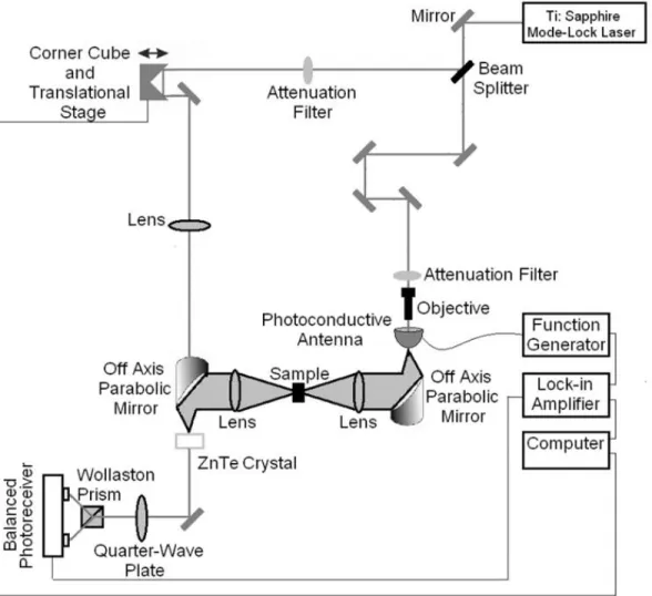
Figure 2.3 CW terahertz reflectance measurement system. To generate CW (0.24 to 0.38 THz) a YIG oscillator integrated with VDI multiplier is used.
15
Figure 2.3 illustrate CW terahertz measurement system that we used in our experiments. The system consists of YIG oscillator as the CW source. YIG stands for yttrium iron garnet, a magnetic crystal with very high quality factor. THz wave generation arises from YIG crystal’s resonant oscillations. When DC magnetic field is applied to YIG crystal, it resonates at microwave frequencies. This response is linear with the applied magnetic field. The YIG oscillator used here can be tuned between 8-13.2 GHz. By employing VDI (Virginia diode) multiplier we were able to generate THz waves with frequency range from 0.24 – 0.38 THz. All components of CW system are movable enabling both transmission and reflection modes of measurements. TPX and teflon lenses are used to collimate and focus the THz wave respectively. The detection is done by employing a Golay cell detector which possess high dynamic range at room temperature.
2.4 Time domain terahertz spectroscopy
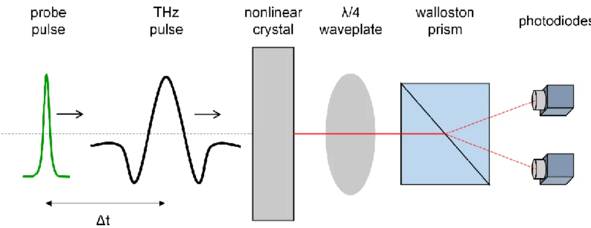
Terahertz time-domain spectroscopy (THz – TDS) is a powerful technique to study physical and chemical processes [30]. In principle, THz – TDS is system where THz pulses are generated and detected at high rate. The detected signal is a time-varying electric field whose Fourier transform produces both amplitude and phase spectra over broad spectral range. Optical parameters of materials are extracted by comparing signals from the sample to a reference signal with known properties. Usually the reference signal is taken in air medium with reduced water vapor molecules. The Figure 2.4 illustrates the scheme of terahertz spectroscopy system. There are various ways to generate and detect terahertz radiations [30]. Most often photoconductive antenna and nonlinear optical crystals are used as emitting and detecting components [29]. According to the schematics, high power, femtosecond duration pulses are engaged to excite and detect THz waves. The echelon of ultra-short pulses are split into two beams by a beam splitter. First beam is sent to terahertz emitter; while the second one is used as probe beam. When the pump pulse hit the THz emitter, the terahertz pulses are excited. These pulses pass through the sample and focus on the
16
THz detector. To readout any signal, the probe pulse and terahertz pulse must both be incident on the THz detector. By sweeping the time delay of the probe pulse the profile of THz beam is extracted (Figure 2.4). To extract the transmitted, reflected, or absorbed spectrum of a sample, the Fourier transform of the terahertz pulses is performed. The refractive index, extinction coefficient, and phase changes of a sample can also be extracted from Fourier transform of the THz pulse. In that sense, time-domain terahertz spectroscopy is an indispensable method to measure optical parameters of materials.
Figure 2.4 Terahertz time-domain spectroscopy (THz-TDS) schematics. Optical beam is split into two pulses. First pulse (pump) impinges on THz emitter (nonlinear crystal, or PC diode) to generate subpicosecond THz pulse. The second pulse (probe) undergoes time delay and impinges on THz detector. The probe pulse is used to gate the THz detector (Schottky diode, PC antenna).
17
The terahertz radiation is generated and detected by PC antennas or nonlinear crystals. The photoconductive antennas can both be utilized as emitters and receivers. The design of the antennas effect the strength and the bandwidth of the resultant terahertz beams. Most common configuration is dipole structure. The figure demonstrates the side view of PC emitter. The two metallic stripes separated by gap sit on substrate. The stripes are illustrated as black protrusions, and are kept at certain bias level. The substrates are semiconductors with fast carrier relaxation time. When the femtosecond pulse impinges on dipole medium, it excites extra charge carriers. The charges are then accelerated by the bias voltage. As result of transient photocurrents, the THz pulse is emitted. The strength and the bandwidth of the emitted THz pulse depends on various parameters.
18
The terahertz emitter is shown in Figure 2.5. It consists of photoconductive antenna and metal contacts. DC bias is applied to coplanar metal-stripes to induce accelerating electric field. Semiconductor with high carrier mobilities and rapid relaxation times are suitable for PC antennas. Most commonly, gallium arsenide (GaAs) or low temperature gallium arsenide (LT-GaAs) are preferred. High mobilities of charge carriers is favorable for the rapid response to electric fields which is crucial for THz pulse excitations. Ultra-short optical pulse excite electron hole pair up on incidence. These pairs are then separated by the DC field resulting in transient current. It is this transient current that induces picosecond terahertz pulses. The bandwidth of the THz pulse dependence on the time duration of pump pulse. Subfemtosecond pulses can excite terahertz pulses with 3 THz bandwidth.
The detection of terahertz pulses with photoconductive antennas are similar in mechanism to emission of the pulses. In this case, both optical pulse and terahertz pulse must be incident on the PC antenna. Figure illustrates the schematic view of PC antenna. Similar design structure is used as with PC emitter. Coplanar metallic stripes are fabricated on semiconductor substrate, Figure 2.6. A probe pulse and terahertz pulse are directed as shown in the figure. The optical pulse upon incidence keeps the semiconductor gated exciting electron hole pairs. In other words, optical pulses changes the state of semiconductor from insulating to conducting by creating charge carriers. Once the terahertz pulse reaches the gated medium, it act as a switch on state inducing current flow between metallic stripes which are picked-up by the detector. Hence, the optimal semiconductor material must have high carrier mobility and short carrier lifetime.
19
Figure 2.6 THz receiver. (a) Probe pulse is impinges on dipole structure of THz receiver causing extra free carriers. When THz pulse hit on dipole structure, it causes detectable photocurrent flow. (b) Side view of THz detector antenna. By changing the time delay, whole electric field profile of THz pulse is mapped out.
20
Figure 2.7 Schematic view of terahertz time domain spectroscopy measuring system. Figure 2.7 show the schematic representations of time-domain terahertz spectroscopy. The mode-lock laser of femtosecond duration pulses is used as the emitter pump and detector probe pulses. The laser beam is split into two. The first beam impinges on photoconductive antenna, figure. The antenna consists of semiconductor medium. When the femtosecond pulses hit the PC antenna, it generates the photocarriers, which are then accelerated by the bias voltage. The terahertz pulses are generated by these transient carriers. The subpicosecond THz pulses are focused on the sample, and falls on THz detector. To detect terahertz pulses another PC antenna can be used. The detection is carried out via nonlinear crystal.
21
Figure 2.8 THz pulse emission in a nonlinear crystal.
Figure 2.8 illustrates the basic scheme for terahertz generation where ultrashort pulses induce THz pulses in nonlinear medium due to optical rectification. In linear systems polarization state is proportional to electric field by the equation 2.1. At nonlinear regime higher order contributions of the susceptibility starts to be significant. When we expand equation 2.1 we end up with higher order terms of electric susceptibility.
The expansion of 𝜒, susceptibility, is represented in the equation 2.2.
The optical rectification and the Pockel’s Effects are the second order nonlinear effects describe by the second term in the equation 2.2. For a field with E = E0cos(ωt), the second order effect is,
P
⃗⃗ = χ(E)E⃗⃗ 2.1
P = χ1E + χ2E2+ χ
22
where second order term of polarization has two components. The first component corresponds to DC, or low frequency, polarization state. The second component is result of second harmonic generations of the crystal. The later has no contribution to optical rectification. Hence, the nonlinear optical rectifications is caused by the DC component of the polarization state.
For fields at different frequencies, E1 = E0cos(ω1t) and E2 = E0cos(ω2t), the
second order polarization is,
Here, we have cos(ω1− ω2) and cos(ω1+ ω2) terms. The higher frequency term
has no contribution to emission or detection. The lower frequency term is a result of the optical rectification effect.
Detection of THz pulses can be done using crystal with second order nonlinear property. The figure demonstrates the basic principles of detecting terahertz pulses. Both probe pulse (with femtosecond pulse duration) and THz pulse must be collinearly incident on nonlinear crystal. When the probe and terahertz pulses coincide in the nonlinear optical medium, the latter pulse changes the refractive index of the medium, which is proportional to the terahertz field amplitude, causes the phase modulation of the probe pulse. Then it passes through quarter waveplate and Wollaston prism to be detected by photodiodes. In other words, variations of the optical medium causes the probe pulse to undergo birefringence. The phase retardation between ordinary and extraordinary pulses are then picked up by the photodiodes, (Figure 2.9). The complete profile of the terahertz pulse is extracted by sweeping the time delay.
P2 = χ2E2 =1 2χ2E0 2(1 + cos(2ωt)) 2.3 P2 = χ2E1E2 = 1 2χ2E0 2(cos(ω 1− ω2)t + cos (ω1+ ω2)t) 2.4
23
Figure 2.9 Electro-optic system to detect terahertz pulses based on nonlinear crystals.
2.5 Graphene-enabled terahertz optoelectronic devices
Graphene is a promising material to be used in terahertz optoelectronics. Many studies already showed the promises of graphene usages in terahertz devices. Graphene mainly was demonstrated as a material to control THz waves. For instance, using graphene enabled field effect transistor Ren et al demonstrated both interband and intraband response of back-gated graphene [37]. Figure 2.10(a) illustrates the devices structure used to study terahertz response of graphene. Their device structure consisted of graphene transferred on SiO2/p-Si substrate. The p-Si was used as the
back-gate, and SiO2 dielectric separating graphene layer. By applying gate voltage
they were able to tune the Fermi energy of graphene from 0.2 to 0.5 eV, and track the changes in mid-infrared and terahertz region. Both THz time-domain spectroscopy and Fourier transform spectroscopy were utilized to measure the transmittance from the graphene device. Ren et al confirmed the Drude-like conductance at terahertz frequencies and also observed the interband transition at mid-infrared region demonstrating strong terahertz activity of graphene. Similar device structure was applied as a THz intensity modulator, Figure 2.10(b). A 20 % modulation was achieved from 570 GHz to 630 GHz frequencies on a single layer graphene device [27]. The modulation is a result of free carrier absorption in graphene. By the same group a reflection type terahertz modulator were developed [48]. In Figure 2.10(c),
24
the graphene enabled resonant device structure is shown. They used back-gating scheme to generate charges on graphene. The device consisted of CVD grown graphene on top of a dielectric, and a evaporated metal on the back of highly doped silicon. By applying bias voltage to gating electrode and graphene they were able to attenuated the terahertz reflectance by 64 % at 620 GHz frequency. These studies demonstrated the feasibility of graphene as an efficient material to manipulate terahertz radiations.
Apart from controlling THz waves, graphene was utilized in terahertz wave detection [26]. Figure 2.10(d) demonstrates the developed terahertz detector based on graphene field effect transistor. By coupling graphene field effect transistor with antenna they were able to achieve responsivity of 100 mV/W. Their device facilitates more efficient and fast terahertz detection at room temperatures. As an application coffee capsules and leaf were imagined in a transmission mode. To produce the images by raster scanning it took 200x550 points, consuming 20 ms for each point. Hence, one image was reproduced at nearly few hundreds seconds which is fast for THz imaging with reasonably good resolution.
25
Figure 2.10 (a) Transistor type graphene device ©2012 ACS [37]. (b) Graphene based THz intensity modulator ©2012 NPG [27]. (c) Reflection type THz intensity modulator ©2012 ACS [48]. (d) Graphene-based field effect THz detector ©2012 NPG [26]. All figures were reprinted with permission from corresponding
publication groups.
2.6 Conclusion
The unique properties such as noninvasive nature, low ionizing energy, high spatial resolution, and wide bandwidth of terahertz waves offer novel opportunities for imaging, communication systems, and other industrial applications. However, low output power of sources, complexity of the terahertz detection systems, and high insertion loss of modulators, switches, and other components limits the wide
26
exploitations in everyday life applications. Graphene has been demonstrated as an efficient material to control and sense terahertz radiations, due to its unique optical and electronic properties. Using graphene as an active material in THz band have a great promise in the realizations of more efficient, compact, cost-effective, and lossless terahertz components.
27
Chapter 3
Optical Properties of Graphene
Graphene is a two-dimensional crystal of carbon atoms with honeycomb lattice structure [2, 49, 50]. Due to its strong interlayer bonding, graphene exhibits high tensile strength and stability at standard conditions. The carbon atoms in the lattice create sigma bonding along the plane and 𝜋 bonding perpendicular to the plane of crystal. These bondings arise from the hybridization of outer shell electrons. Carbon has four electrons in its outer orbitals. Valence electrons are distributed filling 2s and 2p orbitals, hence resulting in sp2 hybridizations. S orbital interacts with only p
x and
py orbitals leaving free perpendicular pz orbital. The three hybridization states of sp2
orbitals results in a hexagonal structure of graphene. So carbon atoms are bonded by in plane sigma bonding exhibiting hexagonal structure. Neighboring pz orbitals
interact with each other creating perpendicular to lattice plane 𝜋-bonding and 𝜋*-antibonding. Moreover, the half-filled pz orbitals are responsible for the conductance


![Figure 2.10 (a) Transistor type graphene device ©2012 ACS [37]. (b) Graphene based THz intensity modulator ©2012 NPG [27]](https://thumb-eu.123doks.com/thumbv2/9libnet/5769665.116956/47.918.188.800.194.852/figure-transistor-graphene-device-graphene-based-intensity-modulator.webp)