Contents lists available atScienceDirect
Optik
journal homepage:www.elsevier.com/locate/ijleo
Original research article
Production and photovoltaic characterisation of n-Si/p-CZTS
heterojunction solar cells based on a CZTS ultrathin active layers
Serap Yiğit Gezgin
a, Amina Houimi
a, Hamdi Şükür Kılıç
b,c,⁎aUniversity of Selçuk, Faculty of Science, Department of Physics, 42031, Selçuklu, Konya, Turkey
bUniversity of Selçuk, Directorate of High Technology Research and Application Center, 42031, Selçuklu, Konya, Turkey
cUniversity of Selçuk, Directorate of Laser Induced Proton Therapy Application and Research Center, 42031, Selçuklu, Konya, Turkey
A R T I C L E I N F O Keywords: Solar cell PLD Ultrathin films CZTS Efficiency Si A B S T R A C T
In this study, Au/n-Si/p-CZTS/Ag solar cells have been produced by using PLD technique. Ultrathin CZTS films have been grown on n-Si wafer in different thicknesses depending on number of laser pulses. These ultrathin CZTS films were analysed by XRD, AFM and UV–vis spectra. J–V characteristics of Au/n-Si/p-CZTS/Ag solar cells have been determined based on thickness of ultrathin CZTS films under AM 1.5 solar radiation of 80 mW/cm2. Short circuit current density (mA/cm2), fill factor, open circuit voltage (V) and power conversion efficiency (%) of ultrathin CZTS film solar cells have been determined for device produced in this work. The photovoltaic (PV) characteristics of ultrathin CZTS film solar cells has been discussed in detail in this present article and, as a result, the ideal ultrathin CZTS film solar cell structure having the highest efficiency has been determined and concluded.
1. Introduction
Second generation solar cells are based on some special materials, such as CdTe and CIGS, with high absorption coefficients and adjustable direct band gaps. However, since these absorber materials consist of expensive (In and Te) and toxic elements (Cd and Ga), the usage of these materials in solar cells are limited [1]. Cu2ZnSnS4(CZTS) structure consists of quartanery component elements, has some preferred properties such as a high absorption coefficient, adjustable direct band gap over 1–1.5 eV range, consisting of non-toxic and inexpensive elements [2]. CZTS is used as alternative to CIGS material due to its similar features in thin film solar cells [3]. Standard thin film solar cells formed with a CZTS absorber layer is usually structured as Al/ITO/i-ZnO/CdS/CZTS/Mo/glass CZTS thin film solar cells, consisting of these layers, contains some adversely features, such as; i- CdS buffer layer is used to form p-n heterojunction which includes a toxic Cd element [4], ii- MoS2layer [5] is formed between Mo and CZTS layer at high sulfurization temperatures forming a barrier for hole transition from CZTS absorber active to Mo rear contact, and generating a series resistance in solar cells, iii- During the formation of solar cell layers, the substrate temperature and/or annealing temperature used can cause layers to be embedded within each other. This may cause some interfacial conditions and defects between layers in solar cells and adversely affect solar cell performance [6,7], vi- KCN solution is used to remove Cu-rich secondary phases, such as Cu2S, CuS formed on the surface of CZTS thin film before production of CdS buffer layer on CZTS layer. However, KCN solution can damage the thin film surface and can cause pin holes in CZTS thin films [8].
In order to overcome all these problems mentioned above, n-type Si wafer can be used instead of n-type CdS buffer layer in CZTS thin film solar cells. n-Si wafer provides some advantages when it is used as a buffer layer in n-Si/p-CZTS hetero junction solar cells.
https://doi.org/10.1016/j.ijleo.2019.163370
Received 30 May 2019; Received in revised form 6 September 2019; Accepted 6 September 2019
⁎Corresponding author at: University of Selçuk, Faculty of Science, Department of Physics, 42031, Selçuklu, Konya, Turkey.
E-mail address:[email protected](H.Ş. Kılıç).
0030-4026/ © 2019 Elsevier GmbH. All rights reserved.
These advantageous may be mentioned as; i- Si wafer is non-toxic material and is abundant in nature [9], ii- CZTS has a tetragonal crystal structure with lattice constants of a = 0.5427 nm and c=1.0848 nm, where Si has a cubic single crystal structure with a lattice constant is 0.5430 nm [10] and, therefore, Si wafer is a highly qualified substrate for epitaxial growth of CZTS thin film [11]. Also, there is very low lattice mismatch between Si and CZTS layer in p-CZTS/n-Si heterojunction [10]. iii- Si wafer is a qualified substrate for deposition of contacts and semiconductor thin films.
CZTS thin film is grown on Si wafer using several techniques such as molecular beam [10], sputtering [12], sol-gel [13] and PLD [14]. PLD is a simple and useful system as well as a flexible technique whose parameters are easily adjustable. Morphologic, optical, crystalline and electrical properties of thin films grown by PLD technique can be controlled during the deposition process by adjusting its parameters, such as laser pulse number, laser fluence, laser wavelength, laser repetition rate, the distance between target and substrate and substrate temperature [15]. The species ablated at high kinetic energy by the laser beam have high mobility and high kinetic energy when they reach the substrate. These species occupy appropriate and stable regions while forming the thin film and make a coherent association with each other, and by proper alignment on the substrate at low temperature, ultimately form a crystalline and epitaxial thin film. The species of the complex material are ejected simultaneously with the laser beam and stoi-chiometric transfer is provided by PLD technique [16–22]. Thus, an ideal thin film can be produced by PLD technique as an interface layer in microelectronic devices.
Thin films with thicknesses below 700 nm are defined to be ultrathin films [19]. Since light directly comes on CZTS layer in Si/ CZTS heterojunction solar cells, CZTS thin film should have ultrathin thickness so that photo excited charge carriers are collected in depletion region without any recombination taken place. In addition, CZTS semiconductor has shorter lifetime of carriers compared to CIGS semiconductor and diffusion length of minority charge carriers is shorter [19,23]. For collection of minority charge carriers in the edge of depletion region, their travel distance should be short enough, because of that, CZTS thin film at low thickness is needed. Therefore, in this study, we have produced ultrathin CZTS films by PLD technique for production of Au/n-Si/p-CZTS/Ag solar cells devices. J–V characteristics of Si/CZTS solar cells were determined under AM (Air Mass) 1.5 solar radiation of 80 mW/cm2. The power conversion efficiency studies of these solar cells were acquired depending on thicknesses of ultrathin CZTS film. Au/n-Si/p-CZTS/Ag solar cells produced with ultrathin CZTS films in thicknesses less than 400 nm have shown PV properties. It is also very striking that ultrathin CZTS film solar cells produced by ultrathin CZTS film in 210 nm thickness which has the power conversion efficiency of 1.15% even though it hasn’t formed by thin film buffer layer. Furthermore, the efficiency study of Au/n-Si/p-CZTS/Ag solar cells produced by ultrathin CZTS films in 61 nm, 112 nm, 210 nm, 242 nm and 313 nm thickness, and Au and Ag metal contacts were performed for the first time in the literature.
Morphological, crystalline and optical characteristics of ultrathin CZTS films based on thin film thicknesses were analysed and interpreted by Atomic force microscope (AFM), Scanning electron microscope-Energy-dispersive ray spectroscopy (SEM-EDX), X-ray Powder Diffraction (XRD) and UV–vis spectra, respectively.
2. Experimental
2.1. The growth of ultrathin CZTS film on Si wafer by PLD
In this study, Au/n-Si/p-CZTS/Ag solar cell was produced using PLD technique, utilizing a Nd: YAG laser at 1064 nm wavelength, 10 Hz repeat rate and 5 ns pulse width. To focus the laser beam on CZTS target material, a convex lens with 50 cm focal length was used. Laser spot size is 0,65 mm and laser fluency has been calculated as 1.1 J/cm2. The experiments were carried out in a vacuum chamber where background pressure can be obtained about 1 × 10⁻⁶mbar.
A n-type Si wafer having ∼10 Ω.cm resistance, (100) crystalline orientation and 500 μm thickness was used as a substrate. The area of Si wafer is 1 cm2. Firstly, Si wafer was cleaned with foam soap and then, left in a mixed solution with hydro-fluoride (HF) and distilled water (1:24) for 2 min to remove the oxide layer from surface of the wafer. After that it was rinsed by distilled water and dried by nitrogen gas.
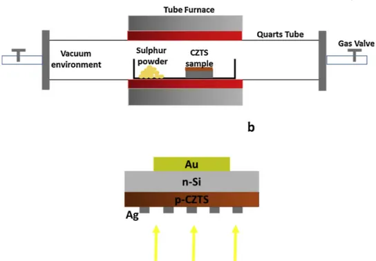
Au thin film contact was deposited on back side of Si wafer while ultrathin CZTS film was grown on front side of Si wafer at room temperature by PLD technique. Prior to run experiment, target-substrate separation and laser energy were set at 45 mm and 15 mJ, respectively. Sputtering target of CZTS (%99,99 purity) was purchased from GoodWill-Chine commercial company ( www.chine-goodwill.com), has been not polished before each experiment and has Cu:Zn:Sn:S (2:1:1:4 at%) element ratios. In order to study ultrathin film thickness dependency, CZTS target material was ablated using 2400, 4800, 7200, 9600 and 12,000 laser pulses and the ultrathin CZTS films were deposited on Si wafer. Sulphide powder of 50 mg was placed next to ultrathin CZTS film and ultrathin CZTS film was annealed at 375 °C and 400 °C (for ultrathin CZTS3 film) temperature for 45 min in vacuum condition in tube furnace as shown inFig. 1a. Ag grid contact was coated on ultrathin CZTS film by Physical Vapour Deposition (PVD) technique. The active area of Au/n-Si/p-CZTS/Ag solar cell is 0.2 cm2and the produced structure of the solar cell is shown inFig. 1b.
2.2. Material characterization
Morphological, crystalline and optical properties of ultrathin CZTS films were analysed by using AFM, SEM-EDX, XRD, Raman spectroscopy and UV–vis spectra, respectively. A RENISHAW Raman Microscope was used for measurements at 532 nm excitation wavelength performed with a laser power of 1.5 mW. The thicknesses of ultrathin CZTS films were measured by Profilometer. J–V electrical characterization of CZTS solar cells were obtained under AM 1.5 solar radiation of 80 mW/cm2. Short circuit current density (Jsc), Filling Factor (FF), Open circuit voltage (Voc) and efficiency (η) of these CZTS solar cells were determined from J–V
characteristics. 3. Discussion
3.1. XRD analysis
Thicknesses of ultrathin CZTS1, CZTS2, CZTS3, CZTS4 and CZTS5 films grown by applying 2400, 4800, 7200, 9600 and 12,000 laser pulses have been determined to be 61 nm, 112 nm, 210 nm, 242 nm and 313 nm, as shown in the plot inFig. 2, respectively. All these ultrathin CZTS films were annealed at 375 °C sulfurization temperature. As the laser pulse number were increased, the thickness of ultrathin CZTS films were increased as indicated inFig. 2[24,25].
The XRD pattern of ultrathin CZTS1, CZTS2, CZTS3, CZTS4 and CZTS5 films are shown inFig. 3a. Ultrathin CZTS films are in polycrystalline structure and in the direction of (112), (200), (220) hkl planes, the diffraction peaks of ultrathin CZTS films appeared at 28°, 33°, 47° (2θ) values [26,27], and ultrathin CZTS films have polycrystalline tetragonal structure (JCPDS Card No: 01-075-4122). Since CZTS1 thin film is very thin, the peak at (112) orientation is very weak while the peak at (200) orientation is more pronounced. However, the intensity of the main peak at (112) orientation increases, as the thickness of thin film increases [28]. The average size of grain forming the thin film is calculated by the Scherrer equation, which is expressed below:
=
D 0.94 / cos (1)
where D is size of grain, is the full-width at half-maximum of diffraction peak, is Bragg diffraction angle, λ is wavelength of X-ray Fig. 1. a) The image of tube furnace and b) schematic structure of Au/n-Si/p-CZTS/Ag solar cell produced by PLD technique.
[29,30]. The average grain sizes forming CZTS1, CZTS2, CZTS3, CZTS4 and CZTS5 ultrathin films annealed at 375 °C temperature have been calculated to be 7.34 nm, 10.71 nm, 17.61 nm, 17.79 nm and 22.25 nm using Scherrer formula, respectively. In addition, average size of ultrathin CZTS3 film at 400 °C temperature is 16.70 nm. As the thickness of ultrathin CZTS film increases, their average grain size increases [28].
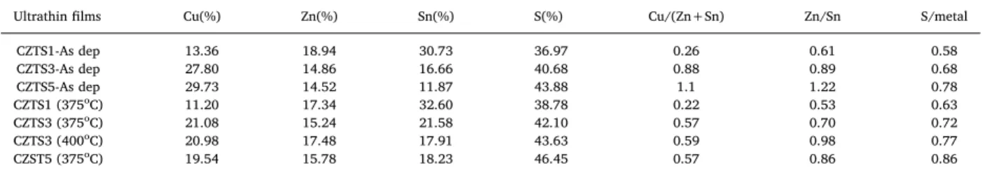
As it will be stated in the section where the PV characterisation of n-Si/p-CZTS solar cells in this study was given, the best solar cell performance has been presented by CZTS3A solar cell produced by ultrathin CZTS3 film. Therefore,Fig. 3b shows a peak pattern of XRD spectrum from ultrathin CZTS3 films which were grown in 210 nm thickness and annealed at 375 °C temperature. For a higher performance of n-Si/p-CZTS solar cells, ultrathin CZTS3 film has been determined as the most ideal absorber ultrathin film. The ultrathin CZTS3 film has a major peak at the highest intensity appeared in (112) orientation. We have experienced this from our previous work [27]. In addition, densities of peaks at (200) and (220) orientations are lower than that of the main peak [31]. Ultrathin CZTS3 film has tetragonal polycrystalline structure (JCPDS Card No: 01-075-4122) [32]. Also, we have taken Raman Spectra for only ultrathin CZTS3 film which has been obtained and shown in inset inFig. 3b. The major peak at 337 cm−1belongs to CZTS phase [9,33,34]. The very weak peaks at 267 cm−1and 290 cm−1are also present and these peaks correspond to Cu2SnS3(CTS) second phase [35]. The presence of CTS phase may be attributed to the fact that the ratio of Sn is higher than Zn ratio (Zn/Sn = 0.7) in CZTS3 thin film, although Cu ratio is slightly lower, as seen inTable 1[36,37].
3.2. Morphological analysis
According to AFM images shown inFig. 4, ultrathin CZTS1 film has the smallest particle sizes. It has been observed that as the number of laser pulses increases, number of ablated particles increases and a large number of CZTS particles arriving on substrate was joined together to increase particle size. So, thickness of ultrathin film increases as size of particles forming ultrathin films increases. Therefore, average particle size of ultrathin CZTS3 film is greater than ultrathin CZTS1 film’s average particle size. In addition, it has been noticed that ultrathin CZTS5 film has the largest particle size compared to other thin films [24,25]. It has also been observed that ultrathin CZTS1 film exhibits almost homogenous particle size distribution, whereas ultrathin CZTS3 and CZTS5 films show non-Fig. 3. XRD patterns of a) ultrathin CZTS1, CZTS2, CZTS3, CZTS4, CZTS5 films annealed at 375 °C and ultrathin CZTS3 film annealed at 400 °C at sulfurization temperature, b) XRD pattern of ultrathin CZTS3 and Raman Spectra of ultrathin CZTS3 film in inset.
homogeneous one.
EDX-Spectra of as-deposited ultrathin CZTS1, CZTS3, and CZTS films, the annealed these ultrathin CZTS films at 375 °C sulfur-ization temperature and ultrathin CZTS3 film annealed at 400 °C sulfursulfur-ization temperature are given inFig. 5. In addition, element ratios of these ultrathin CZTS films are expressed inTable 1.
Ultrathin CZTS films are generally Cu poor but Zn and Sn rich [19,38], according to atomic ratios of elements given inTable 1and Fig. 5. In this study, CZTS material has been ablated by applying low laser energies to prevent droplets in thin films and ablation of CZTS material with low laser energy causes ultrathin CZTS films to be Cu poor. So, the ablation threshold value of Cu element was exceeded with low laser energies but the ablated Cu content was low [19]. Possibility of formation of VCu(Cu vacancy) and ZnCu acceptor defects and SnZndonor defect structures in these ultrathin CZTS films is high. VCuand ZnCudefect structures result in some increases in p-type property of CZTS thin film. SnZndonor defect decreases p-type property of CZTS thin film and adversely affects performance of ultrathin CZTS film solar cells [39–41]. CZTS structure is Cu-poor and Zn-rich for CZTS solar cells have high-efficiency [42]. In this study, VCuand ZnCuacceptor defects in ultrathin CZTS film can cause increasing hole charge carrier con-centration [3]. In addition, Cu/Sn ratios are lower to ultrathin CZTS films produced, can lead to longer life time for minority carriers in ultrathin CZTS films [43]. This can ensure that both Jscand efficiency values of CZTS solar cells are slightly higher although CZTS thin films are the ultrathin. Furthermore, Cu element ratio decreased and Sn element ratio increased in the annealed ultrathin CZTS films compared to as-deposited ultrathin CZTS films. Zn element ratio increased in annealed ultrathin CZTS3 and CZTS5 films. This difference in element ratio is based on sulfurization annealed temperature. The sulfurization annealing temperature of 375 °C is not a high temperature for the evaporation of Sn element [44,45]. However, Sn atoms can exhibit a higher diffusivity towards the surface of the thin film than other metal atoms at 375 °C annealing temperature [44]. Sulfur pressure can also be high and can result in the presence of large amounts of Sn atoms on the surface [46,47]. In addition, when sulfurization temperature for ultrathin CZTS3 thin film was increased from 375 °C to 400 °C to optimize the component ratio, Zn ratio increased and Sn ratio decreased. As the sul-furization temperature increased, Sn atoms evaporated [48,49]. Thus, Cu/(Zn + Sn) and Zn/Sn ratios increased to approximate the ideal CZTS thin film component [3].
3.3. Optical characterization of ultrathin CZTS films
As thickness of ultrathin CZTS film increases, absorption density of these films increases as seen from absorbance spectra given in Fig. 6a. While thickness of ultrathin CZTS film increases, particle size of ultrathin films increases and their transparency decreases. Thus, ultrathin CZTS film absorbs more photons.
Band gap of thin films can be calculated using Tauc law expressed below:
=
hv A hv E
( )2 ( g)1/2 (2)
Where, A is constant, Egis thin film band gap, hv is energy of photon. Egis obtained by extrapolation of linear line of hv( )2versus hv
( )in Tauc plot as shown inFig. 6b. Band gap values for ultrathin CZTS1, CZTS2, CZTS3, CZTS4 and CZTS5 films were determined to be 1,95 eV, 1,90 eV, 1,56 eV 1,50 eV and 1,45 eV according to Tauc plot inFig. 6b, respectively, [50]. The band gaps of these ultrathin CZTS films are in agreement with the literature [28]. Furthermore, It is well known from literature that band gap of ideal CZTS film is about 1.5 eV. Ultrathin CZTS4 film has the ideal band gap, while ultrathin CZTS3 and CZTS5 films are close to the ideal band gap. However, band gaps of these ultrathin CZTS1 and CZTS2 films are found higher since thicknesses and average grain size of these ultrathin films are very low and smaller, respectively [3,50]. As thickness and average grain size of ultrathin films increases, ab-sorption rate of ultrathin films increases while band gap values decrease [27].
3.4. The PV characterizations of n-Si/p-CZTS solar cells
Fig. 7. indicates that J–V characteristics of n-Si/p-CZTS solar cells depend on thickness and annealed temperature of ultrathin CZTS films. All CZTS solar cells produced with ultrathin CZTS films has exhibited PV properties under AM 1.5 solar radiation of 80 mW/cm2. The PV characteristics of ultrathin CZTS film solar cells are given inTable 2.
Jsc, Voc, FF and η parameters of CZTS1A solar cell produced by ultrathin CZTS1 film with average grain size of 7.34 nm were determined to be 1.6 mA/cm2, 100 mV, 0.30 and 0.06%, respectively. CZTS2A solar cell formed by ultrathin CZTS2 film have an Table 1
Atomic ratios of elements in as deposited ultrathin CZTS1, CZTS3 and CZTS5 films, ultrathin CZTS1, CZTS3, CZTS5 films annealed at 375 °C sulfurization temperature, ultrathin CZTS3 film annealed at 400 °C sulfurization temperature.
Ultrathin films Cu(%) Zn(%) Sn(%) S(%) Cu/(Zn+Sn) Zn/Sn S/metal CZTS1-As dep 13.36 18.94 30.73 36.97 0.26 0.61 0.58 CZTS3-As dep 27.80 14.86 16.66 40.68 0.88 0.89 0.68 CZTS5-As dep 29.73 14.52 11.87 43.88 1.1 1.22 0.78 CZTS1 (375oC) 11.20 17.34 32.60 38.78 0.22 0.53 0.63 CZTS3 (375oC) 21.08 15.24 21.58 42.10 0.57 0.70 0.72 CZTS3 (400oC) 20.98 17.48 17.91 43.63 0.59 0.98 0.77 CZST5 (375oC) 19.54 15.78 18.23 46.45 0.57 0.86 0.86
Fig. 4. AFM images (3 μm × 3 μm area) are given for a) CZTS1, b) CZTS3 and c) CZTS5 ultrathin films in 61 nm, 210 nm and 313 nm thickness, respectively.
average grain size of 10.71 nm and exhibits electric parameters to be Jsc= 11.85 mA/cm2, Voc= 180 mV, FF = 0.18 and η = 0.53%. CZTS3A (375 °C) solar cell was produced based on ultrathin CZTS3 film active layer (annealed at 375 °C temperature) with average grain size 17.61 nm and gives values for parameters to be Jsc= 14.50 mA/cm2, Voc= 240 mV, FF = 0.26 and η = 1.15% [3]. Ul-trathin CZTS3 film annealed at 400 °C sulfurization temperature has grain size of 16.70 nm and the photovoltaic parameters of the CZTS3A (400 °C) solar cell produced with this ultrathin CZTS3 film are Jsc= 15.31 mA/cm2, Voc= 280 mV, FF = 0.21 and η= 1.13% Ultrathin CZTS4 film has a particle size of 17.79 nm and CZTS4A solar cell produced with this active layer exhibits Jsc= 13.49 mA/cm2, Voc= 210 mV, FF = 0.21 and η = 0.71% parameter values. CZTS5A solar cell produced based on ultrathin CZTS5 film with average grain size of 22.25 nm and gives values for parameters determined to be Jsc= 10.57 mA/cm2, Voc= 200 mV, FF = 0.24 and η = 0.63%. The highest power conversion efficiency among these ultrathin CZTS film solar cells is given by CZTS3A solar cell, while CZTS1A solar cell has the lowest power conversion efficiency.
CZTS1A solar cell produced with the lowest Jscvalue of 1.60 mA/cm2, while CZTS3A solar cell has the highest value for Jscand measured to be 14.50 mA/cm2. Since ultrathin CZTS1 absorber layer in solar cell was very thin with a 61 nm thickness, no enough Fig. 5. EDX-Spectra of as deposited ultrathin a) CZTS1, c) CZTS3, f) CZTS5 films ultrathin b) CZTS1, d) CZTS3, g) CZTS5 films at 375 °C sulfurization temperature, e) ultrathin CZTS3 film at 400 °C sulfurization temperature.
photon absorption were performed by this absorber layer [51]. Also, the crystal structure of ultrathin CZTS1 film is quite poor which indicates that there are many defect structures in ultrathin CZTS1 film. These defects can act as recombination points for minority charge carriers and result in decreasing the lifetime of minority carriers. So, they can result in a high series resistance and, therefore, Jscvalue to be low [52]. As thickness of ultrathin CZTS films increases, their crystal structures were improved to cause some increases in average grain sizes. Thus, defect structures that act to be recombination points for photo excited charge carriers are passivized and lifetime of charge carriers increases [4] and this results in an increase in Jscvalue. CZTS2A and CZTS3A solar cells have absorber layers in 112 nm and 210 nm thicknesses, respectively, Jscvalues has steadily increased [28,53,54]. Also, the photon numbers ab-sorbed by absorber layer and photo-current increases with increasing thicknesses of ultrathin CZTS films. This situation causes Jsc value to increase. Although CZTS2 and CZTS3 thin films have ultrathin thickness, their short circuit current densities are high [28,53,54]. Because diffusion length of the photo-excited charge carriers can be longer than thicknesses of ultrathin CZTS films, lifetime of charge carriers are longer. The photo-excited minority charge carriers can diffuse to depletion region without too much
Fig. 6. a) Absorption spectra and b) Tauc plot of ultrathin CZTS1, CZTS2, CZTS3, CZTS4, CZTS5 films.
Fig. 7. J–V characteristics of n-Si/p-CZTS solar cells depending on thickness of and annealed temperature of ultrathin CZTS films under illumination condition.
Table 2
The PV characteristics of n-Si/p-CZTS solar cells depending on thickness and annealed temperature of ultrathin CZTS films.
Sample Ultrathin CZTS film thickness Jsc Voc FF η
CZTS1A 61 nm 1.60 mA/cm2 100 mV 0.30 0.06% CZTS2A 112 nm 11.85 mA/cm2 180 mV 0.18 0.53% CZTS3A (375oC) 210 nm 14.50 mA/cm2 240 mV 0.26 1.15% CZTS3A (400oC) 213 nm 15.31 mA/cm2 280 mV 0.21 1.13% CZTS4A 242 nm 13.49 mA/cm2 210 mV 0.21 0.71% CZTS5A 313 nm 10.57 mA/cm2 200 mV 0.24 0.63%
recombination [23]. As the annealing temperature for ultrathin CZTS3 film increased from 375 °C to 400 °C, Jscand Vocvalues of CZTS3A (400 °C) solar cell increased. Since the element ratios of ultrathin CZTS3 (400 °C) film component have been optimized, some defects in thin ultrathin film can be passivized which cause to increased in Jscand Vocvalue. The efficiencies of CZTS3A (375 °C; η= 1.15%) and CZTS3A (400 °C; η = 1.13%) solar cells are very close to each other, due to the decrease in FF value. However, although thickness of the absorber layer in CZTS4A and CZTS5A solar cell increases to 242 nm and 313 nm, respectively, Jscvalues of CZTS4A and CZTS5A solar cells decrease down to 13.49 mA/cm2and 10.57 mA/cm2, respectively [55]. In fact, as thicknesses of these thin films increase and their crystal structures are developed, Jscvalues can be expected to be higher, but, it is decreased compared to Jscvalue of CZTS3A solar cell. Because of incident light came directly on ultrathin CZTS film, the photo-exited charge carriers are formed near the Ag contact, and the minority charge carriers tend to recombine in this contact. Also, while thickness of thin film increases, number of photo-excited charge carriers increases, but diffusion length of formed minority carriers may be probably shorter than thickness [23]. This limits the access of the minority charge carriers to the depletion region. So, these charge carriers can recombine before they reach in depletion region and thus Jscand Vocvalues decrease [55]. As a result, Jsc, Vocand η values of ultrathin CZTS solar cells increased when thicknesses of CTZS thin films were increased from 61 nm to 210 nm, this electrical values decreased while the ultrathin film thickness was increased from 210 nm to 313 nm. So, PV parameters of n-Sİ/p-CZTS solar cells have changed in accordance with each other, depending on the thickness of ultrathin CZTS films.
Low Vocof CZTS solar cells can be attributed to some reasons. To exhibit ohmic behaviour of Ag grid contact for p-type CZTS thin films, work function of Ag metal should be greater than work function of p-type CZTS [56]. Ag contact cannot exhibit a good ohmic behaviour for CZTS since work function of Ag metal contact (4.6 eV) [57] is lower than work function of CZTS thin film (5.1 eV) [21] High contact resistance of Ag metal results in high series resistance [58,59]. In addition, since work function of Au metal (5.1 eV) [57] is greater than that of n-type Si wafer(4.6 eV) [57], Au contact causes a high contact resistance and series resistance [56,60,61]. Therefore, a high contact resistance results in Vocvalue to be low [58].
An oxide layer is likely to be formed on Si wafer, and this oxide layer results in an interfacial state, some defects and traps between Si and CZTS layers [62,63]. Traps and defects in a site of depletion region acts as a recombination point for charge carriers, leakage current occurs in the depletion region and charge collection is limited in edge of depletion region. Thus, Vocvalue remains low [14]. In addition, band alignment between CZTS and Si semiconductors can adversely affect hole transition from CZTS to Si wafer. This limitation in charge transmission causes a low Vocvalue [9,14].
Because CZTS ultra-thin films are very thin, pinholes and cracks may occur in ultrathin films when they are annealed at sul-furization temperature, and this can cause leakage current in CZTS solar cells and some lower shunt resistance. Thus, Vocvalues decreases [57,64–66]. In addition, some low shunt and high series resistance result in a low FF value for all CZTS solar cells [14]. Consequently, the highest efficiency has been given by CZT3A solar cell which have an active layer having 210 nm thickness, while the lowest efficiency has been obtained by CZTS1A solar cell using an active layer thickness of 61 nm. When thickness of ultrathin CZTS film has been increased beyond 210 nm, Jsc, Vocand therefore η values have been increased. But, when the thickness of ultrathin film has been increased from 210 nm to 313 nm, Jscand Vocvalues have been decreased. Therefore, it was found that the effect of Jscand Vocon these efficiency of CZTS solar cells is very significant.
4. Conclusion
In this study, Au/n-Si/p-CZTS/Ag solar cells were produced depending on thickness of ultrathin CZTS films. As number of laser pulse increases, average grain size and thickness of ultrathin CZTS films increases. Since average grain size increases, crystalline structures and absorption rates of ultrathin CZTS films were progressively developed and increased, respectively. In studies of ul-trathin CZTS film solar cells depending on thickness of ulul-trathin CZTS films, CZTS1A solar cell was produced based on ulul-trathin CZTS1 film measured to be 61 nm in thickness has shown the lowest efficiency, while CZTS3A solar cell produced based on ultrathin CZTS3 film in 210 nm thickness has given the highest efficiency. In addition, the efficiency of CZTS3A (400 °C) solar cell produced by annealing ultrathin CZTS3 film at 400 °C was found very close to the efficiency of CZTS3A (375 °C) solar cell. Although Jscvalue of all ultrathin CZTS film solar cells are slightly higher, its Vocand FF value are slightly low. Metals having appropriate work function should be used to form ohmic contact and provide low contact resistance with semiconductors to increase Vocand FF values. Laser energy (laser fluency) was used to ablate CZTS target material should be set at a more appropriate value to the stoichiometric transfer of ultrathin CZTS films.
Acknowledgements
Authors kindly would like to thank,
The Scientific and Technological Research Council of Turkey (TUBITAK) for financial support via Grant No. 1649B031503748, - Selçuk University, High Technology Research and Application Center for supplying with Infrastructure and
- Selçuk University, Scientific Research Projects Coordination (BAP)Unit for grands via projects with references of 18401178, 18401124 and 15201070.
References
[1] X. Song, et al., A review on development prospect of CZTS based thin film solar cells, Int. J. Photoenergy 2014 (2014). [2] T.P. Dhakal, et al., Characterization of a CZTS thin film solar cell grown by sputtering method, Sol. Energy 100 (2014) 23–30.
[3] M.-Y. Yeh, et al., Copper-zinc-tin-sulfur thin film using spin-coating technology, Materials 9 (7) (2016) p. 526.
[4] G.K. Dalapati, et al., Impact of molybdenum out diffusion and interface quality on the performance of sputter grown CZTS based solar cells, Sci. Rep. 7 (1) (2017) p. 1350.
[5] K.J. Yang, et al., Effects of Na and MoS2 on Cu2ZnSnS4 thin‐film solar cell, Prog. Photovolt. Res. Appl. 23 (7) (2015) 862–873.
[6] K. Tanaka, et al., Cu2ZnSnS4 thin film solar cells prepared by non-vacuum processing, Sol. Energy Mater. Sol. Cells 93 (5) (2009) 583–587. [7] C. Yan, Developing High Efficiency Cu2ZnSnS4 (CZTS) Thinfilm Solar Cells by Sputtering, (2016).
[8] T. Ericson, Sputtering of Precursors for Cu2ZnSnS4 Solar Cells and Application of Cadmium Free Buffer Layers, Acta Universitatis Upsaliensis, 2018. [9] S. Singh, et al., Superior heterojunction properties of solution processed copper-zinc-tin-sulphide quantum dots on Si, Nanotechnology 28 (43) (2017) 435704. [10]N. Song, et al., Epitaxial Cu2ZnSnS4 thin film on Si (111) 4 substrate, Appl. Phys. Lett. 106 (25) (2015) 252102.
[11]N. Song, Epitaxial Growth of Cu2ZnSnS4 Thin Films, (2015).
[12]J. Xu, et al., Preparations of Cu2ZnSnS4 thin films and Cu2ZnSnS4/Si heterojunctions on silicon substrates by sputtering, Opt. – Int. J. Light Electron. Opt. 127 (4) (2016) 1567–1571.
[13]S. Patel, J. Gohel, Effect of type of solvent on the sol–gel spin coated CZTS thin films, Phys. Astron. Int. J. 1 (4) (2017) p. 00023.
[14]Z.O. Elhmaidi, et al., Pulsed laser deposition of CZTS thin films, their thermal annealing and integration into n-Si/CZTS photovoltaic devices, 2016 International Renewable and Sustainable Energy Conference (IRSEC), IEEE, 2016.
[15]A. Moholkar, et al., Synthesis and characterization of Cu2ZnSnS4 thin films grown by PLD: solar cells, J. Alloys Compd. 509 (27) (2011) 7439–7446. [16]A.C. Cazzaniga, et al., Fabrication of Thin Film CZTS Solar Cells With Pulsed Laser Deposition, Technical University of Denmark (DTU), 2016. [17]A.O. Dikovska, et al., Thin ZnO films produced by pulsed laser deposition, J. Optoelectron. Adv. Mater. 7 (2005) 1329–1334.
[18]C.M. Ghimbeu, et al., Crystalline vanadium nitride ultra-thin films obtained at room temperature by pulsed laser deposition, Surf. Coat. Technol. 211 (2012) 158–162.
[19]A. Cazzaniga, et al., Ultra-thin Cu2ZnSnS4 solar cell by pulsed laser deposition, Sol. Energy Mater. Sol. Cells 166 (2017) 91–99. [20]M. Beres, et al., Stoichiometry control in Cu2ZnSnS4 thin films grown by pulsed laser deposition, Mater. Chem. Phys. 205 (2018) 90–96.
[21]R. Pandiyan, et al., Reconstructing the energy band electronic structure of pulsed laser deposited CZTS thin films intended for solar cell absorber applications, Appl. Surf. Sci. 396 (2017) 1562–1570.
[22]J. Schou, Physical aspects of the pulsed laser deposition technique: the stoichiometric transfer of material from target to film, Appl. Surf. Sci. 255 (10) (2009) 5191–5198.
[23]F. Liu, et al., Beyond 8% ultrathin kesterite Cu 2 ZnSnS 4 solar cells by interface reaction route controlling and self-organized nanopattern at the back contact, NPG Asia Mater. 9 (7) (2017) e401.
[24]M. Đekić, et al., Influence of deposition parameters on pulsed laser deposition of K0. 3MoO3 thin films, Bull. Chem. Technol. Bosnia and Herzegovina 48 (1) (2017) 1.
[25]Z. Vakulov, et al., Size effects in LiNbO3 thin films fabricated by pulsed laser deposition, J. Phys. Conf. Ser. (2018) 1124.
[26]S.M. Camara, L. Wang, X. Zhang, Easy hydrothermal preparation of Cu2ZnSnS4 (CZTS) nanoparticles for solar cell application, Nanotechnology 24 (49) (2013) p. 495401.
[27]S.Y. Gezgin, H. Kiliç, The electrical characteristics of ITO/CZTS/ZnO/Al and ITO/ZnO/CZTS/Al heterojunction diodes, Optik (2019).
[28]J. Tao, et al., A sputtered CdS buffer layer for co-electrodeposited Cu 2 ZnSnS 4 solar cells with 6.6% efficiency, Chem. Commun. 51 (51) (2015) 10337–10340. [29]R.K. Jamal, M.A. Hameed, K.A. Adem, Optical properties of nanostructured ZnO prepared by a pulsed laser deposition technique, Mater. Lett. 132 (2014) 31–33. [30]R. Khandelwal, et al., Effects of deposition temperature on the structural and morphological properties of SnO2 films fabricated by pulsed laser deposition, Opt.
Laser Technol. 41 (1) (2009) 89–93.
[31]S. Rondiya, et al., Effect of calcination temperature on the properties of CZTS absorber layer prepared by RF sputtering for solar cell applications, Mater. Renew. Sustain. Energy 6 (2) (2017) 8.
[32]N.A. Bakr, Z.T. Khodair, H.I. Mahdi, Influence of thiourea concentration on some physical properties of chemically sprayed Cu2ZnSnS4 thin films, Int. J. Mater. Sci. Appl. 5 (2016) 261–270.
[33]X. Fontané, et al., Selective detection of secondary phases in Cu 2 ZnSn (S, Se) 4 based absorbers by pre-resonant Raman spectroscopy, 2013 IEEE 39th Photovoltaic Specialists Conference (PVSC), IEEE, 2013.
[34]S.-N. Park, et al., Solution-processed Cu 2 ZnSnS 4 absorbers prepared by appropriate inclusion and removal of thiourea for thin film solar cells, RSC Adv. 4 (18) (2014) 9118–9125.
[35]S.R. Kodigala, Thin Film Solar Cells From Earth Abundant Materials: Growth and Characterization of Cu2 (ZnSn)(SSe) 4 Thin Films and Their Solar Cells, Newnes, 2013.
[36]W. Bao, M. Ichimura, Influence of secondary phases in kesterite-Cu2ZnSnS4 absorber material based on the first principles calculation, Int. J. Photoenergy 2015 (2015).
[37]D.M. Berg, et al., Discrimination and detection limits of secondary phases in Cu2ZnSnS4 using X-ray diffraction and Raman spectroscopy, Thin Solid Films 569 (2014) 113–123.
[38]C. Kim, S. Hong, Optical and electrical properties of Cu2ZnSnS4 thin films grown using spray pyrolysis technique and annealing in air, Mol. Cryst. Liq. Cryst. 645 (1) (2017) 217–224.
[39]S. Chen, et al., Structural, electronic and defect properties of Cu 2 ZnSn (S, Se) 4 alloys, MRS Online Proc. Libr. Arch. (2011) 1370.
[40]D. Han, et al., Deep electron traps and origin of p-type conductivity in the earth-abundant solar-cell material Cu 2 ZnSnS 4, Phys. Rev. B 87 (15) (2013) p. 155206.
[41]L. Yin, et al., Limitation factors for the performance of kesterite Cu 2 ZnSnS 4 thin film solar cells studied by defect characterization, RSC Adv. 5 (50) (2015) 40369–40374.
[42]R. Chen, et al., Efficiency enhancement of Cu2ZnSnS4 solar cells via surface treatment engineering, R. Soc. Open Sci. 5 (1) (2018) p. 171163. [43]C. Yan, et al., Boost Voc of pure sulfide kesterite solar cell via a double CZTS layer stacks, Sol. Energy Mater. Sol. Cells 160 (2017) 7–11. [44]W. Feng, et al., Influence of annealing temperature on CZTS thin film surface properties, J. Electron. Mater. 46 (1) (2017) 288–295.
[45]G.K. Gupta, V. Reddy, A. Dixit, Impact of excess and disordered Sn sites on Cu2ZnSnS4 absorber material and device performance: a 119Sn Mössbauer study, Mater. Chem. Phys. 225 (2019) 410–416.
[46]L. Yao, et al., Reactive mechanism of Cu2ZnSnSe4 thin films prepared by reactive annealing of the Cu/Zn metal layer in a SnSex+ Se atmosphere, Crystals 9 (1) (2019) p. 10.
[47]J. Zhong, et al., Sulfurization induced surface constitution and its correlation to the performance of solution-processed Cu 2 ZnSn (S, Se) 4 solar cells, Sci. Rep. 4 (2014) p. 6288.
[48]A. Emrani, P. Vasekar, C.R. Westgate, Effects of sulfurization temperature on CZTS thin film solar cell performances, Sol. Energy 98 (2013) 335–340. [49]M. Olgar, Optimization of sulfurization time and temperature for fabrication of Cu2ZnSnS4 (CZTS) thin films, Superlattices Microstruct. 126 (2019) 32–41. [50]P. Dai, et al., Band-gap tunable (Cu2Sn) x/3 Zn 1− x S nanoparticles for solar cells, Chem. Commun. 46 (31) (2010) 5749–5751.
[51]F. Mollica, Optimization of Ultra-thin Cu (In, Ga) Se2 Based Solar Cells With Alternative Back-contacts, Université Pierre et Marie Curie-Paris VI, 2016. [52]X. Sheng, et al., Low-cost fabrication of Cu 2 ZnSnS 4 thin films for solar cell absorber layers, J. Mater. Sci. Mater. Electron. 24 (2) (2013) 548–552. [53]B. Hartiti, H.J.T. Nkuissi, S. Fadili, Enhancement of Output Parameters of Cu2ZnSnS4 (CZTS)-based Solar Cells: Numerical simulation using AMPS-1D and
SCAPS-1D programs, (2019).
[54]H. Heriche, et al., Thickness optimization of various layers of CZTS solar cell, J. New Technol. Mater. 277 (1747) (2014) 1–4. [55]M. Espindola-Rodriguez, et al., Bifacial kesterite solar cells on FTO substrates, ACS Sustain. Chem. Eng. 5 (12) (2017) 11516–11524.
[56] S. Cui, Metal-Semiconductors Contacts, (2016)https://eng.libretexts.org/Bookshelves/Materials_Science/Supplemental_Modules_(Materials_Science)/ Semiconductors/Metal-Semiconductors_Contacts.
[57]O. Akpa, et al., Chalcopyrite/Si heterojunctions for photovoltaic applications, J. Electron. Mater. 39 (11) (2010) 2462–2466.
[58]D. Bhattacharya, A. Mansingh, P. Swarup, Dependence of series resistance on operating current in pn junction solar cells, Sol. Cells 18 (2) (1986) 153–162. [59]F. Boutebakh, et al., Electrical properties and back contact study of CZTS/ZnS heterojunction, Opt. – Int. J. Light Electron. Opt. 144 (2017) 180–190. [60]E. Ayyildiz, C.N. Lu, A. Türüt, The determination of the interface-state density distribution from the capacitance-frequency measurements in Au/n-Si Schottky
barrier diodes, J. Electron. Mater. 31 (2) (2002) 119–123.
[61]C.-Y. Chen, et al., Above 10% efficiency earth-abundant Cu2ZnSn (S, Se) 4 solar cells by introducing alkali metal fluoride nanolayers as electron-selective contacts, Nano Energy 51 (2018) 597–603.
[62]H. Afify, et al., Realization and characterization of ZnO/n-Si solar cells by spray pyrolysis, Egypt. J. Solids 28 (2) (2005) 243–254. [63]K.K. Mohamed, Improved performance of ZnO/n-Si solar cells, AL Rafdain Eng. J. 18 (3) (2010) 19–28.
[64]O. Breitenstein, et al., Influence of defects on solar cell characteristics, Solid State Phenomena, Trans Tech Publ., 2010. [65]M. Nath, et al., Factors limiting the open-circuit voltage in microcrystalline silicon solar cells, EPJ Photovolt. 2 (2011) p. 20101.
[66] C. Honsberg, a.S. Bowden, Impact of Both Series and Shunt Resistance, (2019) https://www.pveducation.org/pvcdrom/solar-cell-operation/impact-of-both-series-and-shunt-resistance.