A 94-GHZ PHASE INVERTER-VARIABLE
GAIN AMPLIFIER IN SiGe BiCMOS
a thesis
submitted to the department of electrical and
electronics engineering
and the graduate school of engineering and science
of bilkent university
in partial fulfillment of the requirements
for the degree of
master of science
By
Yi˘
git AYDO ˘
GAN
July, 2017
I certify that I have read this thesis and that in my opinion it is fully adequate, in scope and in quality, as a thesis for the degree of Master of Science.
Abdullah Atalar (Advisor)
I certify that I have read this thesis and that in my opinion it is fully adequate, in scope and in quality, as a thesis for the degree of Master of Science.
Fatih ¨Omer ˙Ilday
I certify that I have read this thesis and that in my opinion it is fully adequate, in scope and in quality, as a thesis for the degree of Master of Science.
Arif Sanlı Erg¨un
Approved for the Graduate School of Engineering and Science:
Ezhan Kara¸san
ABSTRACT
A 94-GHZ PHASE INVERTER-VARIABLE GAIN
AMPLIFIER IN SiGe BiCMOS
Yi˘git AYDO ˘GAN
M.S. in Electrical and Electronics Engineering Supervisor: Abdullah Atalar
July, 2017
Phased array radar systems are capable of steering the beam of radio waves electronically by adjusting the gain and phase of each antenna element as desired. In order to achieve that, each element has to have gain/phase control and these parameters have to be controlled separately. In W-Band designs, constant gain-360◦ phase control is difficult to achieve due to parasitic effects of high frequencies which may quickly differ across different settings. Dividing the phase control task into different blocks in system eases the design difficulties. A well developed W-Band technology SiGe BiCMOS is also crucial to achieve high frequencies and system control.
In this thesis, a 94-GHz SiGe BiCMOS phase inverter with variable gain ampli-fier is developed. Single bit-180◦ phase inversion enables to use multiple bit-180◦ phase shifter which is easier to design in W-Band. In addition to that, variable gain amplifier allows to use this circuit in phased array systems for amplitude tapering to achieve desired beam forming.
Keywords: phased array, phase inverter, variable gain amplifier, SiGe BiCMOS, W-Band.
¨
OZET
94-GHZ SIGE BICMOS TEKNOLOJ˙IS˙INDE FAZ
EV˙IREC˙I-DE ˘
G˙IS
¸T˙IR˙ILEB˙IL˙IR KAZANC
¸ L˙I
Y ¨
UKSELTEC
¸
Yi˘git AYDO ˘GAN
Elektrik ve Elektronik M¨uhendisli˘gi, Y¨uksek Lisans Tez Y¨oneticisi: Abdullah Atalar
Temmuz, 2017
Faz dizili radar sistemleri her anten elemanının kazancını ve fazını istenilen ¸sekilde ayarlayarak radyo dalgalarının y¨on¨un¨u elektronik olarak kontrol etme ¨
ozelli˘gine sahiptirler. Bunu yapabilmek i¸cin, her elemanın kazan¸c/faz kontrol¨u olması ve bu parametrelerin birbirlerinden ayrı olarak kontrol edilebilmesi gerek-mektedir. W-Bant tasarımlarda, y¨uksek frekansların farklı ayarlarda de˘gi¸sebilen parazitik etkilerinden dolayı sabit kazan¸c-360◦ faz kontrol¨u elde etmek zordur. Faz kontrol g¨orevini sistemdeki farklı bloklara b¨olmek, tasarım zorluklarını ko-layla¸stırmaktadır. ˙Iyi geli¸stirilmi¸s W-Bant SiGe BiCMOS teknolojisi de y¨uksek frekans ve sistem kontrol¨u icin hayati ¨onem ta¸sımaktadır.
Bu tezde, 94-GHz SiGe BiCMOS tabanlı de˘gi¸stirilebilir kazan¸clı faz evireci geli¸stirilmi¸stir. Tek bit-180◦ faz evirme i¸slemi W-Bant’ta daha kolay tasar-lanabilen ¸coklu bit-180◦ faz kaydırıcı kullanımını sa˘glamı¸stır. Buna ek olarak, istenilen sinyal h¨uzmesini ve y¨on¨un¨u elde edebilmek i¸cin de˘gi¸stirebilir kazan¸c y¨ukselteci bu devrenin faz dizili sistemlerde kullanılabilmesini sa˘glamı¸stır.
Anahtar s¨ozc¨ukler : faz dizili, faz evireci, de˘gi¸stirebilir kazan¸c y¨ukselteci, SiGe BiCMOS, W-Bant.
Acknowledgement
I would like to express my deepest gratitude to my advisor Prof. Dr. Abdullah Atalar for his guidance, supervision and providing me the opportunity to develop my thesis and complete my graduate education while I was working at Aselsan and IBM.
I would like to thank my thesis jury, Prof. Dr. Fatih ¨Omer ˙Ilday and Prof. Dr. Arif Sanlı Erg¨un for reviewing and evaluating my thesis.
I would also like to express my gratitude to Ahmet Aktu˘g for his support and valuable advices on microwave circuit design. I am also grateful to Ahmet Soydan Akyol, S¸ebnem Saygıner and O˘guz S¸ener for trusting me and providing the opportunity of work at IBM where I designed the circuit in this thesis.
I would like to thank Dr. Alberto Valdes Garcia for providing his tremendous amount of knowledge in mm-wave area. I also want to thank my colleagues Wooram Lee, Jean-Oliver Plouchart and C¸ a˘glar ¨Ozda˘g for answering all of my questions and helping me to understand mm-wave IC design.
Finally, I would like to thank to my parents and my beautiful wife M¨uge for their endless support and love. I am lucky to have you.
Contents
1 Introduction 1
1.1 General Introduction . . . 1
1.2 mm-waves . . . 2
1.3 SiGe BiCMOS Technology . . . 3
1.4 Thesis Outline . . . 3
2 mm-wave Design Fundamentals 4 2.1 Crucial Elements to Achieve First-Time-Right Design . . . 5
2.1.1 Well Modeled Technology . . . 5
2.1.2 High Performance Technology . . . 5
2.1.3 Good Parasitic Extraction Decks and Tools . . . 6
2.1.4 Bug-free Design Kit . . . 6
2.1.5 Good Interaction with Foundry . . . 7
2.1.6 Corner Simulations . . . 7
CONTENTS vii
2.2 Key Design Features Where mm-wave Differs From Microwave . . 8
2.2.1 Transmission Lines . . . 8
2.2.2 Cascode Structure . . . 10
2.2.3 Simulation Flow . . . 11
3 A 94-GHz SiGe BiCMOS Phase Inverter-Variable Gain Ampli-fier Design 13 3.1 Single-bit 180◦ Phase Control . . . 14
3.2 Variable Gain Amplifier . . . 19
3.2.1 Biasing and Varying the Gain . . . 21
3.3 Parasitic Modeling and Layout Considerations . . . 22
3.4 Simulation Results for Overall Circuit Across Corners . . . 24
4 Measurement 31 4.1 Setup . . . 31
4.2 Measurement Results . . . 36
List of Figures
2.1 A microstrip line . . . 9
2.2 A CPW line . . . 9
2.3 A half-CPW half-microstrip line . . . 10
2.4 Common-emitter common-base cascode configuration . . . 11
2.5 Crossing of two signals at different layers . . . 12
3.1 Shunt switching structure . . . 14
3.2 Shunt switching structure with additional λ/4 tlines . . . 15
3.3 Short and open characteristics of 0◦ branch . . . 16
3.4 Short and open characteristics of 180◦ branch . . . 16
3.5 Shunt switching structure with additional λ/common tlines . . . . 17
3.6 Short and improved open characteristics of 0◦ branch . . . 18
3.7 Short and improved open characteristics of 180◦ branch . . . 18
3.8 Two cascode variable gain amplifiers . . . 19
3.9 s11, s21 and s22 plots of cascode gain amplifier at rectangular plot in dB . . . 20
LIST OF FIGURES ix
3.10 s11, s22 plots of cascode gain amplifier at smith chart . . . 20
3.11 Current mirror schematic . . . 21
3.12 Block diagram of biasing . . . 21
3.13 s11, s22 plots of cascode gain amplifier at smith chart . . . 22
3.14 Parasitic modeling of switch . . . 23
3.15 Parasitic modeling of layout . . . 23
3.16 Block diagram of phase inverter-variable gain amplifier . . . 24
3.17 Schematic of the simulated circuit . . . 25
3.18 Layout of the simulated circuit . . . 25
3.19 Nominal corner, min. gain setting, s-parameters . . . 27
3.20 Nominal corner, max. gain setting, s-parameters . . . 27
3.21 Slow corner, min. gain setting, s-parameters . . . 28
3.22 Slow corner, max. gain setting, s-parameters . . . 28
3.23 Fast corner, min. gain setting, s-parameters . . . 29
3.24 Fast corner, max. gain setting, s-parameters . . . 29
4.1 Block diagram of measurement setup . . . 32
4.2 RF Probes at left (a), DC probe at right (b) . . . 34
4.3 CS-5 calibration kit . . . 34
4.4 Probes are landing on IC . . . 35
LIST OF FIGURES x
4.6 Core PI-VGA at right (a), measured circuit (b) . . . 36
4.7 Simulation results of core PI-VGA . . . 37
4.8 Simulation results of measured circuit . . . 37
4.9 Comparison of small-signal analysis of simulation and measure-ment of two samples from 90 to 98 GHz . . . 39
List of Tables
3.1 Simulation corner definition . . . 26
3.2 S-parameters and P1dB simulation results at 94 GHz . . . 30
4.1 Blocks at measurement setup . . . 31
Chapter 1
Introduction
1.1
General Introduction
Phased arrays can be defined as circuits that enable to steer the beam electroni-cally and rapidly. This operation is done by adjusting the phase and amplitude of the signals of the individual elements. Many advantages of phased arrays made them popular such as not moving the structures to beam to different directions, fast-electronically controlled beam forming and high yield numbers since systems can tolerate single element failures [1].
System components inside of the phased arrays should provide different key features. In this thesis, one of them is addressed and tried to be solved; constant gain 360◦ phase inversion. At system level, one can calculate the phase and amplitude of each element to achieve desired beam forming. Constant gain 360◦ phase control separates phase and gain parameters from each other and provides precise phase control to system level designers. Gain control is usually done by multi-bit controlled attenuators and sometimes by adjusting the gain of amplifiers. Reliable phase and gain control of the integrated circuit enables to get high quality images from different directions in small intervals.
technology considering it’s maturity (other circuits are already developed at lower frequencies as in [2], [3], [4]), high frequency performance and capability of pro-ducing complementary metal oxide semiconductors (CMOS) on chip to build analog/digital control circuitry.
1.2
mm-waves
mm-wave frequencies are defined as the frequency range between 30 and 300 GHz. Its getting more and more popular due to high demand of higher data rate communications such as 5G. In terms of data rate, mm-wave designs present capability of achieving 1 Gb/s communication rates [5] thanks to higher operating frequency and open a new era of communication systems. In addition to that, mm-waves are also popular in imaging systems since it provides higher resolution. Increased resolution attracted developers from different majors and mm-wave enters in different areas such as medical, adaptive cruise control and aircraft landging surveillance systems [6]. Also higher frequencies enable us to build smaller and closer antennas which can be directly integrated on package [7].
At the mm-wave spectrum, attenuation of a signal usually increases with fre-quency due to water vapor and oxygen. At some frequencies attenuation increases due to resonance behaviour of these particles [8]. This can be desirable for indoor applications to limit the range but also might be undesirable for the outdoor applications such as surveillance radars. Particularly 94-GHz is popular among imaging applications and used in different circuits such as transmitters, receivers or sensors as in [6], [9], [10] since there is not any extra resonance behaviour of particles in air and the frequency is high enough to benefit from it’s advantages. The circuit in this thesis is going to be used in such application therefore 94 GHz is selected as operating frequency.
1.3
SiGe BiCMOS Technology
Silicon-germanium (SiGe) BiCMOS technology is first developed at 1996 provid-ing the capability of producprovid-ing heterojunction bipolar transistors (HBTs) with CMOS transistors on the same substrate which is SiGe. High fT and fmax
val-ued bipolar transistors are used in RF/mm-wave circuits while CMOS technology which contains NMOS and PMOS transistors is used in analog/digital circuitry. Particularly in civilian applications, SiGe BiCMOS is desired over III-V technol-ogy since it provides higher integration level which leads to build unique system architectures and lower cost. Although new technology solutions such as GaN HEMTs, GaAs HEMTs and InP HBTs have capability of work on mm-wave fre-quencies their cost and integration level haven’t reached SiGe BiCMOS yet [11]. Reliability level is one of the most important factors in complex integrated cir-cuit designs. Without well-established process and design kit it is impossible to achieve simulated performance on real life.
In this thesis, IBM’s 130 nm SiGe BiCMOS 8XP technology is used (IBM sold the foundry to GlobalFoundries during to development stages of 8XP). At 1.7 V operation 260 GHz fT and 320 GHz fmax values are reported for HBTs which is
adequate for 94-GHz designs[8]. 8XP technology is recently became commercially available and provided reliable HBT performance. The circuit in this thesis pro-duced through multi-project wafer fabrication of MOSIS IC Fabrication Service Provider.
1.4
Thesis Outline
In this thesis, design and measurement of a 94-GHz phase inverter-variable gain amplifier in SiGe BiCMOS is presented. In chapter 2, some of the key features and techniques of mm-wave designs are explained. Design steps and simulation results are presented in chapter 3. Measurement setup and results are explained in chapter 4.
Chapter 2
mm-wave Design Fundamentals
Since mm-wave band is the frequency spectrum just above the microwave band, typical RF/microwave design techniques are still valid. However, due to increased parasitic effects designer should only use stable and mathematically well estab-lished procedures such as impedance transformations, input/output matching of transistor and bias point calculations. At the same time, designer should avoid not well calculated procedures as much as possible such as EM analysis, single transistor amplifiers due to parasitic collector-base capacitance and interconnec-tions which are not modeled. Some soluinterconnec-tions of the problems above may reduce the performance, however stable first-time-right design is the most important fea-ture to achieve considering high production costs. In this thesis, these solutions and their effects on performance are discussed time to time with possible more risky solutions and reasons of their risk.
In this chapter, the techniques where mm-wave designs differ from standard RF/microwave designs are discussed. Simulation flow is also reviewed to give the impression of what should be done to start and complete a mm-wave design.
2.1
Crucial Elements to Achieve
First-Time-Right Design
First-time-right design can be defined as achieving desired/simulated performance at measurement of first run of produced chips. Satisfying this goal is important in terms of cost and time, since every other iteration requires significant amount of time and money to be spent. Some of the items in this section is also valid for RF/microwave circuits but some of them are special for mm-wave or has to be considered more carefully.
2.1.1
Well Modeled Technology
From the lowest frequencies to mm-wave probably the most important factor to build successful design is model-to-hardware correlation. Most of the immature technologies and foundries cannot provide well modeled technologies. Because of that, even if they offer high performance technology and show their capability of producing it, hardware must be modeled correctly so that designer can trust simulations.
The circuit in this thesis is one of the very first designs produced with 8XP technology. However, 8XP technology can be seen as the updated version of 8HP technology (fT fmaxvalues are slightly greater, noise figure is slightly lower) where
successful designs are already reported at mm-wave [12][13].
2.1.2
High Performance Technology
When the technology performance is higher, designer can apply techniques such as matching according to reflections rather than noise or power, to make the design more robust in case models are slightly off. Since this frequency range is not as popular as microwave band, obtaining a robust working design is more important than pushing the limits of technology.
2.1.3
Good Parasitic Extraction Decks and Tools
In order to achieve good simulation-hardware correlation, designer should pay attention to use design kit models as much as possible especially at RF signal line. However, some interconnections must be drawn without using design kit models in layout such as transition from upper layer metal to lower layers. Furthermore, transistor performance can be directly affected from adjacent metals or other layout layers. Therefore, parasitics at these areas must be extracted carefully by designer and a design tool should be capable of doing it. Considering all of the features of an electronic design automation (EDA), extraction tool is the most expensive feature since it calculates lots of effects together and provide correct parasitic parameters to designer to be work on.
2.1.4
Bug-free Design Kit
Design kits usually contain bugs; some of them are minor and solvable but some of them are major and make the design unworkable. Of course, decreasing the num-ber of bugs always in favor of designers, however in mm-wave complex circuitries there are two important tools that have to be as much bug-free as possible; DRC (Design Rule Check) and LVS (Layout Versus Schematic).
Usually foundry provides Design Rules to tell designers what they can pro-duce and what they cannot according to their production capabilities. These rules divided into three sections; Class A, B and C rules. Class C rules can be considered as notifications to designers telling that foundry can produce the lay-out as it is however designer should be aware of the situation which affect the performance or reliability. Class B rules can still be omitted however foundry does not approve to produce them since the corresponding layout area carry high risk to affect performance. Class A rules mean foundry cannot produce the layout in that form, designer should change it. These rules have to be defined correctly so that designer can know what is producible and what is not. In addition to that, well-defined Class B and C errors provide designer to capability of manip-ulating layout to achieve desired performance and completing final layout with
some possible errors.
LVS is a tool that compares layout and schematic netlists and show if the layout completely corresponds to the schematic. A single or few-layer desings such as MMICs usually do not require LVS since all connections can be checked easily. However, when the number of layers increases, it is difficult to keep track of all connections especially in large designs. Although the operation of this tool seems easy, it can still carry bugs. Removing those bugs will assure designer that he is simulating exactly what he is going to produce. A single small error may end up with wrong produced IC which costs a lot.
2.1.5
Good Interaction with Foundry
As designers try to improve their designs, technology development teams in foundries also try to improve their processes and design kits. Routinely they release updates for design kits and try to improve hardware-model correlation and decrease the number of bugs. However, new updates can bring new bugs or some features that result in different simulation results compared to previous kit. If designer is in close interaction with foundry these problems can be addressed quickly and he/she can continue to work rather than spend extra time to under-stand and solve that problem. The importance of this item further increases if the technology used is relatively new such as in 8XP technology.
2.1.6
Corner Simulations
In research based works, usually people tend to present the performance of single chip/circuit. However in real life, the performance of chips may differ according to different parameters, the most significant ones are process variation, temperature and voltage supply value. Although temperature and voltage supply value can be kept as constant at measurements, process variation is out of control. Designer should keep in mind that his design may encounter with some variation and he should adjust his design to satisfy the requirements independent of variation.
When a design turns into a real life product and starts to be used in different locations, temperature and voltage supply value also come into picture. Design can be expected to work at sunny weather and snowy weather at the same time. Voltage supply value may also change to some degree.
In order to consider all of these effects together, simulating all combinations of these parameters may not be feasible. Thus, a designer can define corners which are combinations of these parameters and complete simulations at those corners. The corner parameters defined for this thesis will be explained in Chapter 3.
2.1.7
Reliable Test Environment
Even if designer pays attention to all other parameters and foundry produces exactly the design in simulations, it has to be verified correctly to ensure it is working properly. At mm-wave frequencies all of the components used in test setup have to be very-well defined. Even a small bend at a cable may affect the performance and change the measured gain. The details of test setup of this thesis will be explained in Chapter 4.
2.2
Key Design Features Where mm-wave
Dif-fers From Microwave
Besides the points mentioned in previous section, there are few design differences at mm-wave compared to microwave circuits. These differences enable to build more reliable circuits and also help to achieve first-time-right design.
2.2.1
Transmission Lines
At microwave frequencies, commonly microstrip lines are used as transmission lines rather than CPW (co-planar waveguide) lines. In Fig. 2.1 and 2.2, pictures
of a microstrip and a CPW line can be seen.
Figure 2.1: A microstrip line
Figure 2.2: A CPW line
When microstrip lines are used, there will be some electro magnetic (EM) coupling effect between the transmission line and circuit elements since signal can radiate freely. In order to capture that, EM analysis should be performed with a CAD tool such as HFSS. However, since this analysis solves a large number of equations the required time increases exponentially when the number of layers increases. More importantly, when a mm-wave circuit is designed on multi layer IC, these EM coupling effects became out of control and they might cause oscil-lations. Thus, it is almost impossible to reflect hardware on software correctly. To overcome this issue, a designer can waive advantages of microstrip lines and use so called half-CPW half-microstrip line which can be seen at figure 2.3.
At this configuration, RF signal line is surrounded by ground plane by 180 degree so that EM lines will end up at well defined ground plane rather than cou-pling to unrelated design components. The vertical ground connection between the lower and upper layer at Figure 2.3 is done by densely manufactured vias.
Figure 2.3: A half-CPW half-microstrip line
Surrounding RF line from upper side is not necessary if RF line is at highest level of metal. If it is not it, has to be surrounded from both sides due to reasons explained.
As it is described in previous pages, this configuration of transmission line has to be well defined by foundry so that designer can use it safely at mm-wave. Removing the effort of EM analysis and possible further tuning operations will save tremendous amount of time and improve the hardware-software correlation.
2.2.2
Cascode Structure
In Fig. 2.4, a common-emitter common-base configuration can be seen. The advantage of this configuration compared to single common-emitter amplifier is the increased isolation between output and input ports. Due to this reason it is very popular among mm-wave designs as in [14], [15], [16]. The transistor that is used as common-base form reduces the multiplication effect of the Miller capaci-tance at common-emitter transistor and makes the circuit easier to stabilize. This multiplication effect comes from the gain of the transistor, however in cascode form the transistor at common-emitter configuration presents low gain therefore small capacitor is obtained at base to collector. At 94 GHz, unwanted feedback loops can be formed if a common-emitter amplifier is used. Thus, this configura-tion is desired although it carries other disadvantages such as requirement of two transistors.
Figure 2.4: Common-emitter common-base cascode configuration
2.2.3
Simulation Flow
Correct simulation flow is also important to realize the desired design and it car-ries slight differences in mm-wave. Firstly, conventional schematic simulations has to be done. Secondly, EM analysis should be performed if the transmission lines are somewhat interacting each other due to design requirements. For in-stance, in Fig. 2.5, two transmission lines are crossing each other at different layers and their half-cpw half-microstrip structure is sacrificied. Areas like this require EM analysis.
Figure 2.5: Crossing of two signals at different layers
After that, device-level parasitic extraction (with QRC tool) has to performed, especially at areas that can affect the circuit performance. Parasitic extraction is mainly used for capturing the parasitics around the active devices since EM anal-ysis cannot be performed around active devices and improving software-hardware correlation on the areas where only passive design kit models are used. As a final step, via inductances has to be added manually since QRC tool we used correctly extracts only resistances and capacitances not inductances. As a rule of thumb, 1 pH inductance is placed for a µm via length.
Chapter 3
A 94-GHz SiGe BiCMOS Phase
Inverter-Variable Gain Amplifier
Design
In this chapter, the design of a 94-GHz SiGe BiCMOS phase inverter with variable gain amplifier is discussed. This circuit was fabricated on 0.13 µm gate length silicon germanium BiCMOS 8XP technology from GLOBALFOUNDRIES (for-merly IBM’s). This thesis work aimed to achieve constant gain single-bit 180◦ phase control and three-bit gain variation across all corners. All simulations and layout design were completed using Cadence software package.
8XP technology was at it’s beta version when this circuit is designed. Foundry released many design kit updates during and after the design process. These updates on design kit models significantly affected the resulting performance, especially at 94 GHz. In this chapter, all simulations are given with latest design kit which is V.1.6.2.3 since foundry claims it is more accurate for representing hardware although the circuit is initally designed at V.1.6.1.0. This damages the effort of achieving first-time-right design, however it did not destroy completely.
3.1
Single-bit 180
◦Phase Control
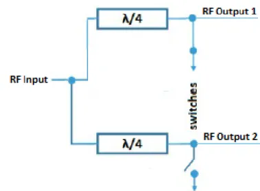
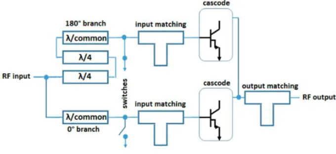
In order to achieve a single-bit phase control, a switching structure can be im-plemented. By this structure, the input signal sees a low impedance at one branch, a high impedance at the other and tends to flow through low impedance one. Switching operation is usually done by PIN diodes, FET transistors or BJT transistors. There are different switch implementations named according to con-nection of switching elements such as series, shunt, series-shunt. Each of them has different advantages and disadvantages on parameters of switches mainly as insertion loss, isolation and bandwidth. In Fig. 3.1, a shunt configuration can be seen. When switching element is OFF, low impedance is transformed as high impedance to the input thanks to λ/4 transmission line and signal flows through the branch where the switching element is ON.
Figure 3.1: Shunt switching structure
This configuration provides good performance on insertion loss since there is no series element, good performance on isolation since it presents low impedance to output port of OFF branch. On the other hand, it has narrow bandwidth since λ/4 transmission line is defined at single frequency. Since there is no bandwidth requriement in our work, this configuration is selected.
In order to create the 180◦ phase difference between branches, two more λ/4 transmission lines are added to one of the branches as shown in Fig. 3.2. This addition won’t change the impedance transformations of that branch since the length of total addition is λ/2 meaning a full rotation in Smith chart. Further-more, since the addition is done at left side of switching elements and output side of branches are identical including switches, next block can be designed together with switches at both branches.
Figure 3.2: Shunt switching structure with additional λ/4 tlines
Main advantage of this technique is using a design kit elements. Other struc-tures such as balun may also provide phase inversion however their performance is always questionable at these frequencies and even more questionable when pack-age effects come into picture. The drawback is extra loss at longer branch due to requirement of travelling longer transmission line. According to simulations, difference is around 0.2 dB which can be considered as acceptable.
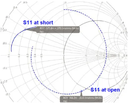
Although this theory sounds great in theory, it needs a slight modification. The ’short’ state of switching elements is not perfectly short due to via induc-tances from transistor layers to signal layer and transistor parasitics at 94 GHz. s11 can be seen in Fig. 3.3 and 3.4 for a short switching element. Poor short
is transformed to poor open at input and due to this desired high impedance at OFF branch can not be achieved.
Figure 3.3: Short and open characteristics of 0◦ branch
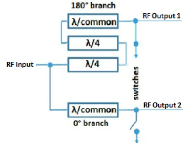
To overcome this issue, a λ/4 transmission line from both branches are shortened to move poor short to a decent open. This length is represented as λ/common in Fig. 3.5. Note that, since one transformation is done by λ/common transmission line and the other is done by λ/common+ λ/2 transmission line, fi-nal s11 points are not exactly the same. In order to show similar high impedances
for OFF branches in both switching cases, the common length was chosen to place the open impedances on both sides equidistant of the real axis. One can twist this selection in the favor of 180◦ branch since 0.2 dB additional loss is expected and our aim is to achieve constant gain at both branches. However, in order to be sure of this technique at 94 GHz, that twist is not done. Improved open at input when λ/common lines are used can be seen in Figs. 3.6 and 3.7 for both branches.
Figure 3.6: Short and improved open characteristics of 0◦ branch
3.2
Variable Gain Amplifier
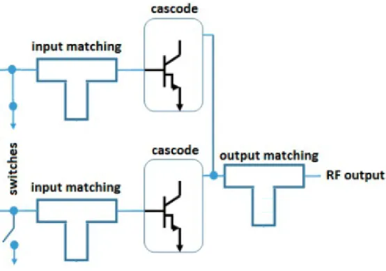
Two identical variable gain amplifiers follow the switch that is described at previ-ous section. Depending on which branch of the switch is active, the other variable gain amplifier is turned off with the same setting in order to prevent unnecessary power consumption. As it can be seen from Fig. 3.8, output matching circuit is shared by two branches since off cascode amplifier presents high impedance at its collector.
Figure 3.8: Two cascode variable gain amplifiers
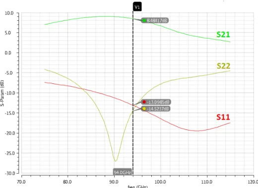
In Fig. 3.9 s11, s22 and s21 values of the circuit in Fig. 3.8 at 94 GHz can be
seen. Note that the notch points of both s11 and s22 are shifted due to design kit
updates although they are designed to be appear at exactly 94 GHz. Nevertheless, both reflections are still under -10 dB. Figure 3.10 shows these reflections on Smith chart.
Figure 3.9: s11, s21 and s22 plots of cascode gain amplifier at rectangular plot in
dB
3.2.1
Biasing and Varying the Gain
Variable gain operation is done by changing the biasing of the amplifier. Cas-code gain amplifier is biased through a current mirror (a simple current mirror circuit is shown in Fig. 3.11) which takes ‘reference current‘ and mirrors it with certain ratio to transistor at common-emitter configuration. Reference current is controllable as it can be seen in Fig. 3.12. It is also generated through current mirror which takes ‘core reference current‘ from outside of the circuit. Current mirror bank consists of different sizes of transistors whose on and off states are determined by 3-bits of gain control setting. Thanks to that, constant core refer-ence current is mirrored to referrefer-ence current which is mirrored again to be used at cascode gain amplifier.
Figure 3.11: Current mirror schematic
In Fig. 3.13, s21 in dB form can be seen according to 8 different possible
settings. Gain varies from 5.44 dB to 8.48 dB.
Figure 3.13: s11, s22 plots of cascode gain amplifier at smith chart
3.3
Parasitic Modeling and Layout
Considera-tions
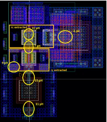
Parasitic modeling is essential to achieve good correlation between software and hardware. As it is described before, after conventional schematic simulations, EM analysis, parasitic extraction and manual addition of parasitic inductances should be performed. In this thesis, there is not any region that requires EM analysis therefore that part is skipped. Secondly, surrounding areas of RF transistors are RC extracted as it can be seen from Fig. 3.14 (switch) and 3.15 (cascode gain amplifier). Finally, unmodeled horizontal and vertical interconnections are manually added as parasitic inductors and they are presented with yellow circles in Fig. 3.14 and 3.15.
Figure 3.14: Parasitic modeling of switch
In simulations, it is observed that the overall performance is very sensitive to parasitic inductance at the base of common-base transistor of cascode amplifier. It is not possible to shorten that length since base of the transistor is at lowest metal layer while the capacitor is at upper layers. Having a long parasitic interconnect at that node might result in unpredicted results. Therefore, in order to reduce the inductance of vertical connection, that via is surrounded by grounded vias. Thanks to that approach, some kind of vertical transmission lines is formed and overall inductance at that point is reduced.
3.4
Simulation
Results
for
Overall
Circuit
Across Corners
In this section, simulation results for overall circuit is presented. The block diagram can be seen in Fig. 3.16 which is combination of switching architecture and variable gain amplifier. The schematic and the layout of the circuit simulated are shown in Figs. 3.17 and 3.18, respectively.
Figure 3.17: Schematic of the simulated circuit
Three corners are defined for the simulations; nominal, slow and fast. Basi-cally, slow corner consists of parameter changes that reduces the gain and vice versa for fast corner. Following parameters are adjusted from corner to corner;
• Temperature. As it is stated at [17], gain of a SiGe HBT decreases when the temperature increases if the base voltage is high due to so called Kirk effect. Since the base voltage of HBTs in this design is high enough, gain decreases with increased temperature. By ensuring slow and fast corner, operation between 0◦ and 85◦ is also ensured which covers possible real life conditions.
• Power supply. Lower power supply values result in less gain. By ensuring slow and fast corner, operation between 2.55 and 2.85 V is also ensured which covers possible fluctiations at DC supply.
• Device performance. This parameter is defined by foundry which tells the possible production variations on transistors. TT means typical, SS means slow, FF means fast.
Corner name Nominal Slow Fast Temperature (◦C) 25 85 0 Power supply (V) 2.7 2.55 2.85 Device performance TT SS FF
Table 3.1: Simulation corner definition
In what follows, S-parameter and P1 dB simulations are presented at nominal, slow and fast corners for minimum and maximum gain setting. Filled squares represent the 0◦ phase shift branch while empty circles represent the 180◦ phase shift branch. In Table 3.2, whole results are represented together.
Figure 3.19: Nominal corner, min. gain setting, s-parameters
Figure 3.21: Slow corner, min. gain setting, s-parameters
Figure 3.23: Fast corner, min. gain setting, s-parameters
Corner Gain PI Setting s21 (dB) s11 (dB) s22 (dB) P1dB (dBm) Nominal Min. 0 4.54 −14.69 −15.59 −6.81 Nominal Min. 180 4.45 −18.74 −15.06 −6.96 Nominal Max. 0 7.71 −16.28 −14.84 1.41 Nominal Max. 180 7.59 −23.69 −14.19 1.40 Slow Min. 0 0.36 −20.33 −13.67 −8.93 Slow Min. 180 0.09 −21.99 −13.46 −9.39 Slow Max. 0 4.27 −22.13 −12.72 −0.27 Slow Max. 180 3.98 −39.17 −12.44 −0.44 Fast Min. 0 7.01 −11.98 −15.55 −3.60 Fast Min. 180 6.93 −15.96 −14.87 −4.42 Fast Max. 0 9.57 −13.69 −15.71 2.15 Fast Max. 180 9.59 −19.54 −14.77 2.11 Table 3.2: S-parameters and P1dB simulation results at 94 GHz
Chapter 4
Measurement
4.1
Setup
Measurement setup consists of the blocks that are given in Table 4.1. The dia-gram of setup can be seen in Fig. 4.1. This setup can perform the small-signal measurement from 10 MHz to 110 GHz.
Model Explanation Quantity
Agilent N5227A Vector Network Analyzer 1 Agilent N5261A mm-wave Head Controller 1 Agilent N5260-60013 mm-wave Head Module for Freq. Extension 2 Agilent N6700B Low - Profile MPS Mainframe 1
SHF DCB-100B DC Block 2
GORE CX0AB0ABC20.0 1mm. cable 2
GGB 110H-GSG-100-P-W RF Probe (GSG) 2 GGB MCW-25-2487-1 DC Probe (PPGPPGPP) 1
Working procedure is as follows; The network analyzer is capable of generating signals up to 67 GHz, therefore another structure is needed for frequencies above. When the frequency is below 67 GHz, network analyzer operates as there is no head modules and controller. When frequency exceeds 67 GHz, higher frequencies are generated at head modules by frequency multiplication controlled by head controller. Network analyzer, head module and head controller is a mm-wave setup solution priovided by Agilent Technologies up to 110 GHz. Generated signal passes through DC block and 1 mm. cable which are both capable of handling 94 GHz signal and presented to chip through GSG (ground-signal-ground) probe (west). The RF probe can be seen in Fig. 4.2 (a). At the output port of the circuit (east) the same RF components are presented.
DC power is supplied from MPS (modular power system) mainframe. It has four outputs; 2.7 V for bias, 0.85 V for generating 50 µA reference current, 0 or 2.7 V for minimizing or maximizing gain setting (3 bits are avaliable for gain setting, they are all connected to this port), 0 or 2.7 V for selecting phase. They are all connected to chip from south side through PPGPPGPP probe (6 power pads; bias, reference current, 3 settings of gain, selecting phase) (P represents power, G stands for ground). The DC probe can be seen in Fig. 4.2 (b).
Calibration of probes is done on the calibration set provided by Picoprobe given in Fig. 4.3. SOLT (short-open-load-through) calibration is completed from 90 to 98 GHz with 200 Hz IF bandwidth.
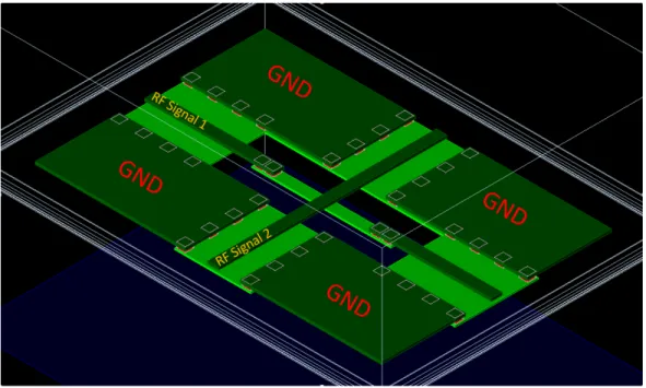
In Fig. 4.4, the picture of the measured circuit can be seen. Note that on top of the layout given in Fig. 3.18, it has extra pads and transmission lines to pads to land appropriate probes. Produced chips are diced by foundry and glued to the copper carrier using thermal epoxy.
In Fig. 4.5, overall setup is presented. This setup is newly built at ASELSAN-REHIS and it is also used for different circuits/measurements therefore it has other blocks around it to perform different measurements.
Figure 4.2: RF Probes at left (a), DC probe at right (b)
Figure 4.4: Probes are landing on IC
4.2
Measurement Results
Remember that all of the simulation results given at Chapter 3 are done with the circuit which has the layout in Fig. 4.6(a). This circuit can be called as ”Core PI-VGA” since it is going to be integrated to higher scale IC and it has to provide certain features such as decent input and output return losses. However, in order to make this circuit measurable, pads for probe landing and additional transmission lines to those pads are necessary. Eventually, these additions mainly change the input and output return losses since the pads introduce significant capacitance at 94 GHz. In Fig. 4.6, layouts of simulated and measured circuits can be seen. In Fig. 4.7 simulation results of core PI-VGA, in Fig. 4.8 simulation results of measured circuit are given at nominal corner, maximum gain. Note that as in Chapter 3, the shapes of small-signal results are similar with some shifting behaviors among corners and gain/phase settings therefore only one of the corners at one setting is shown to give the main idea.
Figure 4.7: Simulation results of core PI-VGA
Two samples of phase inverter-variable gain amplifier are measured. Their results at 94 GHz are presented at table 4.2.
IC Number Gain PI Setting s21 (dB) s11 (dB) s22 (dB) Phase (◦)
1 Min. 0 4.33 −10.49 −17.45 121.94 1 Min. 180 4.00 −10.27 −18.85 −62.39 1 Max. 0 6.84 −10.62 −15.90 117.05 1 Max. 180 7.01 −10.16 −17.44 −67.21 2 Min. 0 4.13 −10.63 −18.22 120.71 2 Min. 180 3.90 −10.44 −19.52 −63.39 2 Max. 0 6.76 −10.66 −16.42 115.72 2 Max. 180 7.02 −10.25 −17.90 −68.27
Table 4.2: Measurement results of two samples
Results above show that PI-VGA works as expected in terms of its most important parameters;
• Phase. For the same sample and gain setting, inverting the phase bit cre-ates a phase difference very close to 180◦ (it is 184◦ approximately). This shows that, phase model of λ/2 transmission line is accurate and 4 degrees can be considered as tolerable. In addition to that, for the same sample and phase setting, minimizing and maximizing the gain creates a phase dif-ference around 5 degrees. If the overall phased array system is considered, this value is acceptable and will not create huge errors at beam directions. Therefore, one can use the variable gain amplifier for tapering purposes safely.
• s21(dB). According to simulation results given at table 3.2, the gain results
map somewhere between nominal and slow corner, closer to the nominal. Also the gain difference between minimum and maximum settings is consis-tent with simulation result which shows that circuit is capable of performing gain adjustment.
In Fig. 4.9, the small-signal analysis of simulation and measurement of two samples from 90 to 98 GHz are shown together where boxes represent the simu-lation, circles and crosses represent the measurement of two samples. From this figure it can be understood that;
• Results of two samples are very close to each other. This increases the confidence on measurement results.
• s21 values match with around 0.5 dB error which is at acceptable level.
• s11values are also close but seem better at measurement (from around −7.2
dB to −10.6 dB).
• s22values show that the frequency of notch is shifted significantly however it
turns out that return losses at measurement are better (from around −11.1 dB to 16 dB).
Figure 4.9: Comparison of small-signal analysis of simulation and measurement of two samples from 90 to 98 GHz
Chapter 5
Conclusion and Future Work
In this work, a 94 GHz phase inverter-variable gain amplifier is designed to be used in a 94 GHz phased array structure. Considering the difficulty of a constant gain-360◦ phase shifter at these frequencies, this circuit is considered to provide constant gain and single bit 180◦ phase control. Some tapering range is desired to be included since gain of indiviual front ends will be adjusted according to desired beam direction at system level.
Circuit is designed at 8XP technology of GLOBALFOUNDRIES, since it is mainly designed to be used in 94 GHz recevier and transmitter ICs at that tech-nology. During the design, design kit models are tried to be used as much as possible and custom structures are avoided. Nevertheless, some areas at layout couldn’t be modeled with design kit such as transistor connections to upper layers, therefore careful parasitic extractions and estimation of parasitic inductances are performed. Overall design is optimized to provide decent gain, input and output return losses at three corners defined.
After the design is completed, in order to measure the circuit at probe station, additional pads and transmission lines are added. Small signal measurements are performed at given setup from 90 to 98 GHz. Measurement results show that circuit operates well in terms of single bit 180◦ phase shifting, gain values and gain tapering. It also provides good input and output return loss, while the notch
of output return loss is shifted.
As a future work, that shift at output return loss can be investigated. The possible candidate is the modeling of the base of common-base transistor at cas-code structure. The reason of it is, that node was sensitive on simulations and a small error at modeling may end up with effecting the circuit. Also, since the shape of s11 is somewhat consistent between simulation and measurement while
the shape of the s22 is not, the problem could be near to the output.
In this thesis, I tried to present not only the circuit but also the important points to pay attention at a mm-wave design. I hope other students can benefit from this thesis in the future if they want to enter this area.
Bibliography
[1] M. I. Skolnik, “Radar Handbook,” 1970.
[2] S. K. Reynolds, B. A. Floyd, U. R. Pfeiffer, T. Beukema, J. Grzyb, C. Haymes, B. Gaucher, and M. Soyuer, “A Silicon 60-GHz Receiver and Transmitter Chipset for Broadband Communications,” IEEE Journal of Solid-State Circuits, vol. 41, no. 12, pp. 2820–2831, 2006.
[3] X. Guan, H. Hashemi, and A. Hajimiri, “A Fully Integrated 24-GHz Eight-element Phased-array Receiver in Silicon,” IEEE Journal of Solid-State Cir-cuits, vol. 39, no. 12, pp. 2311–2320, 2004.
[4] A. Natarajan, A. Komijani, and A. Hajimiri, “A Fully Integrated 24-GHz Phased-array Transmitter in CMOS,” IEEE Journal of solid-state circuits, vol. 40, no. 12, pp. 2502–2514, 2005.
[5] Niknejad, Ali M and Hashemi, Hossein, mm-Wave Silicon Technology: 60 GHz and Beyond. Springer Science & Business Media, 2008.
[6] R. Appleby and R. N. Anderton, “Millimeter-wave and Submillimeter-wave Imaging for Security and Surveillance,” Proceedings of the IEEE, vol. 95, no. 8, pp. 1683–1690, 2007.
[7] Y. P. Zhang and D. Liu, “Antenna-on-chip and Antenna-in-package Solutions to Highly Integrated Millimeter-wave Devices for Wireless Communications,” IEEE Transactions on Antennas and Propagation, vol. 57, no. 10, pp. 2830– 2841, 2009.
[8] H. J. Liebe, “MPM An Atmospheric Millimeter-wave Propagation Model,” International Journal of Infrared and millimeter waves, vol. 10, no. 6, pp. 631–650, 1989.
[9] E. Moldovan, S.-O. Tatu, T. Gaman, K. Wu, and R. G. Bosisio, “A new 94-GHz Six-port Collision-avoidance Radar Sensor,” IEEE Transactions on Microwave Theory and Techniques, vol. 52, no. 3, pp. 751–759, 2004.
[10] J. W. May and G. M. Rebeiz, “Design and Characterization of W -band SiGe RFICs for Passive Millimeter-wave Imaging,” IEEE Transactions on Microwave Theory and Techniques, vol. 58, no. 5, pp. 1420–1430, 2010.
[11] G. Carlson, “Trusted Foundry: the Path to Advanced SiGe Technology,” in Compound Semiconductor Integrated Circuit Symposium, 2005. CSIC’05. IEEE. IEEE, 2005, pp. 4–pp.
[12] A. Natarajan, A. Valdes-Garcia, B. Sadhu, S. K. Reynolds, and B. D. Parker, “W -Band Dual-Polarization Phased-Array Transceiver Front-End in SiGe BiCMOS,” IEEE Transactions on Microwave Theory and Techniques, vol. 63, no. 6, pp. 1989–2002, June 2015.
[13] A. Natarajan, S. K. Reynolds, M. D. Tsai, S. T. Nicolson, J. H. C. Zhan, D. G. Kam, D. Liu, Y. L. O. Huang, A. Valdes-Garcia, and B. A. Floyd, “A Fully-Integrated 16-Element Phased-Array Receiver in SiGe BiCMOS for 60-GHz Communications,” IEEE Journal of Solid-State Circuits, vol. 46, no. 5, pp. 1059–1075, May 2011.
[14] B. Floyd, S. Reynolds, U. Pfeifer, T. Beukema, J. Grzyb, and C. Haymes, “A Silicon 60 GHz Receiver and Transmitter Chipset for Broadband Com-munications,” in Solid-State Circuits Conference, 2006. ISSCC 2006. Digest of Technical Papers. IEEE International. IEEE, 2006, pp. 649–658.
[15] A. Tessmann, A. Leuther, C. Schwoerer, H. Massler, S. Kudszus, W. Reinert, and M. Schlechtweg, “A Coplanar 94 GHz Low-noise Amplifier MMIC Using 0.07/spl mu/m Metamorphic Cascode HEMTs,” in Microwave Symposium Digest, 2003 IEEE MTT-S International, vol. 3. IEEE, 2003, pp. 1581– 1584.
[16] T. Yao, M. Q. Gordon, K. K. Tang, K. H. Yau, M.-T. Yang, P. Schvan, and S. P. Voinigescu, “Algorithmic Design of CMOS LNAs and PAs for 60-GHz Radio,” IEEE Journal of Solid-State Circuits, vol. 42, no. 5, pp. 1044–1057, 2007.
[17] A.-S. Peng, K.-M. Chen, G.-W. Huang, M.-H. Cho, S.-C. Wang, Y.-M. Deng, H.-C. Tseng, and T.-L. Hsu, “Temperature Effect on Power Characteristics of SiGe HBTs,” in 2004 IEEE MTT-S International Microwave Symposium Digest (IEEE Cat. No.04CH37535), vol. 3, June 2004, pp. 1955–1958 Vol.3.